


 Loading...
bq24133
www.ti.com |
SLUSAF7B –DECEMBER 2010 –REVISED MAY 2011 |
1.6-MHz Synchronous Switch-Mode Li-Ion and Li-Polymer Stand-Alone Battery Charger with Integrated MOSFETs and Power Path Selector
Check for Samples: bq24133
FEATURES
•1.6MHz Synchronous Switch-Mode Charger with 2.5A Integrated N-MOSFETs
•Up to 92% Efficiency
•30V Input Rating with Adjustable Over-Voltage Protection
–4.5V to 17V Input Operating Voltage
•Battery Charge Voltage
–1, 2, or 3-Cell with 4.2V/Cell
•High Integration
–Automatic Power Path Selector Between Adapter and Battery
–Dynamic Power Management
–Integrated 20-V Switching MOSFETs
–Integrated Bootstrap Diode
–Internal Loop Compensation
–Internal Digital Soft Start
•Safety
–Thermal Regulation Loop Throttles Back Current to Limit Tj = 120°C
–Thermal Shutdown
–Battery Thermistor Sense Hot/Cold Charge Suspend & Battery Detect
–Input Over-Voltage Protection with Programmable Threshold
–Cycle-by-Cycle Current Limit
•Accuracy
–±0.5% Charge Voltage Regulation
–±5% Charge Current Regulation
–±6% Input Current Regulation
•Less than 15μA Battery Current with Adapter
Removed
•Less than 1.5mA Input Current with Adapter Present and Charge Disabled
•Small QFN Package
–3.5mm × 5.5mm QFN-24 Pin
APPLICATIONS
•Tablet PC
•Netbook and Ultra-Mobile Computers
•Portable Data Capture Terminals
•Portable Printers
•Medical Diagnostics Equipment
•Battery Bay Chargers
•Battery Back-Up Systems
DESCRIPTION
The bq24133 is highly integrated stand-alone Li-ion and Li-polymer switch-mode battery charger with two integrated N-channel power MOSFETs. It offers a constant-frequency synchronous PWM controller with high accuracy regulation of input current, charge current, and voltage. It closely monitors the battery pack temperature to allow charge only in a preset temperature window. It also provides battery detection, pre-conditioning, charge termination, and charge status monitoring. The thermal regulation loop reduces charge current to maintain the junction temperature of 120°C during operation.
The bq24133 charges a one, two, or three cell Li-Ion battery in three phases: precondictioning, constant current, and constant voltage.
Charge is terminated when the current reaches 10% of the fast charge rate. A programmable charge timer offers a safety back up. The bq24133 automatically restarts the charge cycle if the battery voltage falls below an internal threshold, and enters a low-quiescent current sleep mode when the input voltage falls below the battery voltage.
The bq24133 features Dynamic Power Management (DPM) to reduce the charge current when the input power limit is reached to avoid over-loading the adapter. A highly-accurate current-sense amplifier enables precise measurement of input current from adapter to monitor overall system power.
Please be aware that an important notice concerning availability, standard warranty, and use in critical applications of Texas
Instruments semiconductor products and disclaimers thereto appears at the end of this data sheet.
PRODUCTION DATA information is current as of publication date. |
Copyright © 2010–2011, Texas Instruments Incorporated |
Products conform to specifications per the terms of the Texas |
|
Instruments standard warranty. Production processing does not |
|
necessarily include testing of all parameters. |
|
bq24133
SLUSAF7B –DECEMBER 2010 –REVISED MAY 2011 |
www.ti.com |
These devices have limited built-in ESD protection. The leads should be shorted together or the device placed in conductive foam during storage or handling to prevent electrostatic damage to the MOS gates.
DESCRIPTION (CONTINUED)
The bq24133 provides power path selector gate driver ACDRV/CMSRC on input NMOS pair ACFET (Q1) and RBFET (Q2), and BATDRV on a battery PMOS device (Q3). When the qualified adapter is present, the system is directly connected to the adapter. Otherwise, the system is connected to the battery. In addition, the power path prevents battery from boosting back to the input.
The bq24170/172 charges the battery from a DC source as high as 17V, including a car battery. The input over-voltage limit is adjustable through the OVPSET pin. The AVCC, ACP, and ACN pins have a 30V rating. When a high voltage DC source is inserted, Q1/Q2 remain off to avoid high voltage damage to the system.
For 1 cell applications, if the battery is not removable, the system can be directly connected to the battery to simplify the power path design and lower the cost. With this configuration, the battery can automatically supplement the system load if the adapter is overloaded.
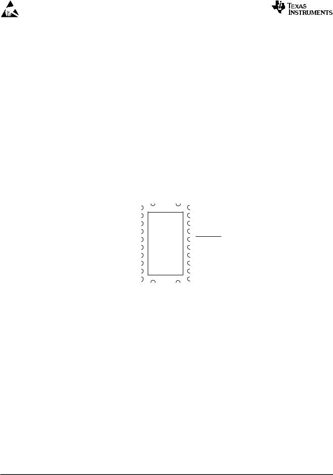
The bq24133 is available in a 24-pin, 3.5mmx5.5 mm thin QFN package.
PVCC
PVCC
AVCC ACN ACP CMSRC ACDRV STAT TS TTC
RGY PACKAGE
(TOP VIEW)
|
|
SW |
|
SW |
|||
|
|
|
|
|
|
|
|
|
|
1 |
|
24 |
|
|
|
2 |
|
|
|
23 |
|||
|
|
|
|
|
|
|
|
3 |
|
|
|
22 |
|||
|
|
|
|
|
|
|
|
4 |
|
|
|
21 |
|||
|
|
|
|
|
|
|
|
5 |
|
|
|
20 |
|||
|
|
|
|
|
|
|
|
6 |
|
|
|
19 |
|||
|
|
|
AGND |
|
|
|
|
7 |
|
|
18 |
||||
|
|
|
|
|
|
|
|
8 |
|
|
|
17 |
|||
|
|
|
|
|
|
|
|
9 |
|
|
|
16 |
|||
|
|
|
|
|
|
|
|
10 |
|
|
15 |
||||
|
|
|
|
|
|
|
|
11 |
|
|
14 |
||||
|
|
|
|
13 |
|
|
|
|
|
|
|
|
|
||
|
|
12 |
|
|
|
|
|
|
|
|
|
|
|
|
|
|
|
VREF |
|
ISET |
|||
PGND
PGND
BTST
REGN
BATDRV OVPSET ACSET SRP SRN CELL
|
|
|
|
PIN FUNCTIONS |
|
PIN |
TYPE |
DESCRIPTION |
|
|
|
|
||
NO. |
|
NAME |
||
|
|
|
||
|
|
|
|
|
1,24 |
|
SW |
P |
Switching node, charge current output inductor connection. Connect the 0.047-µF bootstrap capacitor |
|
|
|
|
from SW to BTST. |
|
|
|
|
|
2,3 |
|
PVCC |
P |
Charger input voltage. Connect at least 10-µF ceramic capacitor from PVCC to PGND and place it as |
|
|
|
|
close as possible to IC. |
4 |
|
AVCC |
P |
IC power positive supply. Place a 1-µF ceramic capacitor from AVCC to AGND and place it as close as |
|
|
|
|
possible to IC. Place a 10-Ω resistor from input side to AVCC pin to filter the noise. For 5V input, a 5-Ω |
|
|
|
|
resistor is recommended. |
5 |
|
ACN |
I |
Adapter current sense resistor negative input. A 0.1-µF ceramic capacitor is placed from ACN to ACP to |
|
|
|
|
provide differential-mode filtering. An optional 0.1-µF ceramic capacitor is placed from ACN pin to AGND |
|
|
|
|
for common-mode filtering. |
|
|
|
|
|
6 |
|
ACP |
P/I |
Adapter current sense resistor positive input. A 0.1-µF ceramic capacitor is placed from ACN to ACP to |
|
|
|
|
provide differential-mode filtering. A 0.1-µF ceramic capacitor is placed from ACP pin to AGND for |
|
|
|
|
common-mode filtering. |
7 |
|
CMSRC |
O |
Connect to common source of N-channel ACFET and reverse blocking MOSFET (RBFET). Place 4-kΩ |
|
|
|
|
resistor from CMSRC pin to the common source of ACFET and RBFET to control the turn-on speed. The |
|
|
|
|
resistance between ACDRV and CMSRC should be 500-kΩ or bigger. |
2 |
Copyright © 2010–2011, Texas Instruments Incorporated |

|
|
|
|
|
|
|
|
|
|
bq24133 |
www.ti.com |
|
|
|
SLUSAF7B –DECEMBER 2010 –REVISED MAY 2011 |
||||||
|
|
|
|
|
|
PIN FUNCTIONS (continued) |
||||
|
|
|
|
|
|
|
|
|
|
|
|
PIN |
TYPE |
DESCRIPTION |
|||||||
|
|
|
|
|
||||||
NO. |
|
|
NAME |
|||||||
|
|
|
|
|
|
|
|
|||
|
|
|
|
|
|
|||||
8 |
|
|
ACDRV |
O |
AC adapter to system switch driver output. Connect to 4-kΩ resistor then to the gate of the ACFET |
|||||
|
|
|
|
|
|
N-channel power MOSFET and the reverse conduction blocking N-channel power MOSFET. Connect |
||||
|
|
|
|
|
|
both FETs as common-source. The internal gate drive is asymmetrical, allowing a quick turn-off and |
||||
|
|
|
|
|
|
slower turn-on in addition to the internal break-before-make logic with respect to the BATDRV. |
||||
|
|
|
|
|
|
|||||
9 |
|
|
STAT |
O |
Open-drain charge status pin with 10-kΩ pull up to power rail. The STAT pin can be used to drive LED or |
|||||
|
|
|
|
|
|
communicate with the host processor. It indicates various charger operations: LOW when charge in |
||||
|
|
|
|
|
|
progress. HIGH when charge is complete or in SLEEP mode. Blinking at 0.5Hz when fault occurs, |
||||
|
|
|
|
|
|
including charge suspend, input over-voltage, timer fault and battery absent. |
||||
|
|
|
|
|
|
|||||
10 |
|
|
TS |
I |
Temperature qualification voltage input. Connect a negative temperature coefficient thermistor. Program |
|||||
|
|
|
|
|
|
the hot and cold temperature window with a resistor divider from VREF to TS to AGND. The temperature |
||||
|
|
|
|
|
|
qualification window can be set to 5-40°C or wider. The 103AT thermistor is recommended. |
||||
11 |
|
|
TTC |
I |
Safety Timer and termination control. Connect a capacitor from this node to AGND to set the fast charge |
|||||
|
|
|
|
|
|
safety timer(5.6min/nF). Pre-charge timer is internally fixed to 30 minutes. Pull the TTC to LOW to disable |
||||
|
|
|
|
|
|
the charge termination and safety timer. Pull the TTC to HIGH to disable the safety timer but allow the |
||||
|
|
|
|
|
|
charge termination. |
||||
|
|
|
|
|
|
|||||
12 |
|
|
VREF |
P |
3.3V reference voltage output. Place a 1-μF ceramic capacitor from VREF to AGND pin close to the IC. |
|||||
|
|
|
|
|
|
This voltage could be used for programming ISET and ACSET and TS pins. It may also serve as the |
||||
|
|
|
|
|
|
pull-up rail of STAT pin and CELL pin. |
||||
13 |
|
|
ISET |
I |
Fast charge current set point. Use a voltage divider from VREF to ISET to AGND to set the fast charge |
|||||
|
|
|
|
|
|
current: |
||||
|
|
|
|
|
|
ICHG = |
VISET |
|
||
|
|
|
|
|
|
20 × RSR |
||||
|
|
|
|
|
|
The pre-charge and termination current is internally as one tenth of the charge current. The charger is |
||||
|
|
|
|
|
|
disabled when ISET pin voltage is below 40mV and enabled when ISET pin voltage is above 120mV. |
||||
|
|
|
|
|
|
|||||
14 |
|
|
CELL |
I |
Cell selection pin. Set CELL pin LOW for 1-cell, Float for 2-cell (0.8V-1.8V), and HIGH for 3-cell with a |
|||||
|
|
|
|
|
|
fixed 4.2V per cell. |
||||
|
|
|
|
|
|
|||||
15 |
|
|
SRN |
I |
Charge current sense resistor negative input. A 0.1-μF ceramic capacitor is placed from SRN to SRP to |
|||||
|
|
|
|
|
|
provide differential-mode filtering. A 0.1-μF ceramic capacitor is placed from SRN pin to AGND for |
||||
|
|
|
|
|
|
common-mode filtering. |
||||
|
|
|
|
|
|
|||||
16 |
|
|
SRP |
I/P |
Charge current sense resistor, positive input. A 0.1-μF ceramic capacitor is placed from SRN to SRP to |
|||||
|
|
|
|
|
|
provide differential-mode filtering. A 0.1-μF ceramic capacitor is placed from SRP pin to AGND for |
||||
|
|
|
|
|
|
common-mode filtering. |
||||
17 |
|
|
ACSET |
I |
Input current set point. Use a voltage divider from VREF to ACSET to AGND to set this value: |
|||||
|
|
|
|
|
|
IDPM = |
|
VACSET |
||
|
|
|
|
|
|
|
|
|||
|
|
|
|
|
|
|
|
20 × RAC |
||
18 |
|
|
OVPSET |
I |
Valid input voltage set point. Use a voltage divider from input to OVPSET to AGND to set this voltage. |
|||||
|
|
|
|
|
|
The voltage above internal 1.6V reference indicates input over-voltage, and the voltage below internal |
||||
|
|
|
|
|
|
0.5V reference indicates input under-voltage. In either condition, charge terminates, and input NMOS pair |
||||
|
|
|
|
|
|
ACFET/RBFET turn off. LED driven by STAT pin keeps blinking, reporting fault condition. |
||||
|
|
|
|
|
|
|
||||
19 |
|
|
|
|
O |
Battery discharge MOSFET gate driver output. Connect to 1kohm resistor to the gate of the BATFET |
||||
|
|
BATDRV |
||||||||
|
|
|
|
|
|
P-channel power MOSFET. Connect the source of the BATFET to the system load voltage node. Connect |
||||
|
|
|
|
|
|
the drain of the BATFET to the battery pack positive node. The internal gate drive is asymmetrical to |
||||
|
|
|
|
|
|
allow a quick turn-off and slower turn-on, in addition to the internal break-before-make logic with respect |
||||
|
|
|
|
|
|
to ACDRV. |
||||
|
|
|
|
|
|
|
||||
20 |
|
|
REGN |
P |
PWM low side driver positive 6V supply output. Connect a 1-μF ceramic capacitor from REGN to PGND |
|||||
|
|
|
|
|
|
pin, close to the IC. Generate high-side driver bootstrap voltage by integrated diode from REGN to BTST. |
||||
21 |
|
|
BTST |
P |
PWM high side driver positive supply. Connect the 0.047-µF bootstrap capacitor from SW to BTST. |
|||||
22,23 |
|
|
PGND |
P |
Power ground. Ground connection for high-current power converter node. On PCB layout, connect |
|||||
|
|
|
|
|
|
directly to ground connection of input and output capacitors of the charger. Only connect to AGND |
||||
|
|
|
|
|
|
through the Thermal Pad underneath the IC. |
||||
|
|
|
|
|
|
|
||||
Thermal |
|
|
AGND |
P |
Exposed pad beneath the IC. Always solder Thermal Pad to the board, and have vias on the Thermal |
|||||
Pad |
|
|
|
|
|
Pad plane star-connecting to AGND and ground plane for high-current power converter. It dissipates the |
||||
|
|
|
|
|
|
heat from the IC. |
||||
|
|
|
|
|
|
|
|
|
|
|
Copyright © 2010–2011, Texas Instruments Incorporated |
3 |
bq24133
SLUSAF7B –DECEMBER 2010 –REVISED MAY 2011 www.ti.com
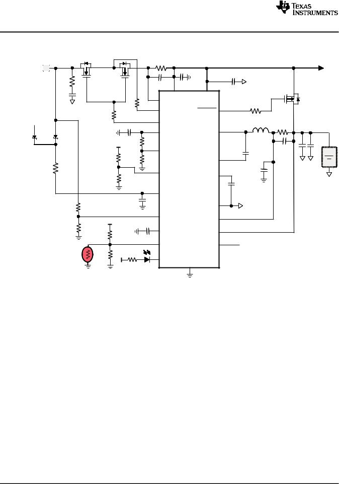
TYPICAL APPLICATIONS
|
Q1 |
|
Q2 |
RAC: 20m |
|
System |
|
|
|
|
|
|
|
|
|
|
|||
12V Adapter |
|
|
|
|
|
C12: 0.1µ |
|
|
|
|
|
|
|
|
|
|
|
|
|
|
RIN |
|
|
C11: 0.1µ |
|
|
|
|
|
|
2 |
|
|
|
|
|
|
||
|
|
|
|
|
|
C4: 10µ |
|
|
|
|
CIN |
|
|
|
|
|
|
|
|
|
|
|
|
ACN |
PVCC |
|
|
|
|
|
2.2? |
|
|
|
R14 |
|
Q3 |
||
|
|
|
|
ACP |
|
|
|||
|
|
|
R12 |
|
|
|
|
||
|
|
|
|
CMSRC |
|
1k |
|
|
|
|
|
R11 |
4.02k |
|
BATDRV |
|
|
|
|
VBAT |
|
|
|
|
|
|
|
|
|
|
4.02k |
|
|
ACDRV |
|
|
|
|
|
|
|
|
C2: 1µ |
|
|
? |
RSR:10m |
|
|
|
|
|
VREF |
|
|
L: 3.3 H |
VBAT |
||
|
|
|
|
VREF |
SW |
|
|
||
D2 |
D1 |
|
|
|
|
|
|
||
|
VREF |
R2 |
|
|
|
|
|
||
|
|
|
bq24133 |
|
|
|
|||
|
|
|
232k |
|
C8 |
|
|||
|
|
|
|
ISET |
|
C5 |
|
||
|
|
|
R4 |
|
|
0.1? |
|
||
|
|
|
|
|
|
0.047? |
|
||
|
|
|
100k |
R3 |
|
BTST |
|
|
|
|
|
|
|
|
|
C9, C10 |
|||
|
R1 |
|
|
32.4k |
|
|
C7 |
|
|
|
10 |
|
R5 |
|
ACSET |
REGN |
0.1? |
|
10? 10? |
|
|
|
32.4k |
|
|
|
|
|
|
|
|
|
|
|
|
|
|
|
|
|
|
|
|
|
|
|
C6 |
|
|
|
|
|
|
C1 |
AVCC |
|
1? |
|
|
|
|
|
|
|
|
|
|
|
|
|
R6 |
|
|
1µ |
|
PGND |
|
|
|
|
1000k |
|
|
|
|
|
|
|
|
|
|
|
|
|
|
|
|
|
|
|
|
|
|
|
OVPSET |
SRP |
|
|
|
|
|
|
C3: 0.1? |
|
|
|
|
||
|
R7 |
VREF |
|
|
|
|
|
||
|
100k |
R8 |
|
|
TTC |
SRN |
|
|
|
|
|
|
|
|
|
|
|
|
|
|
|
5.23k |
|
|
TS |
CELL |
Float |
|
|
|
RT |
|
R10 |
|
|
|
|||
|
R9 |
|
|
|
|
|
|
||
|
1.5k |
|
THERMAL |
|
|
|
|||
|
30.1k |
|
|
|
|
||||
|
103AT |
|
|
STAT |
PAD |
|
|
|
|
|
|
VREF |
D3 |
|
|
|
|||
|
|
|
|
|
|
|
|
||
Figure 1. Typical Application Schematic (12V input, 2 cell battery 8.4V, 2A charge current, 0.2A pre-charge/termination current, 2A DPM current, 18V input OVP, 0 – 45°C TS)
4 |
Copyright © 2010–2011, Texas Instruments Incorporated |

|
|
|
|
|
|
|
|
|
|
|
|
|
|
bq24133 |
www.ti.com |
|
|
|
|
|
|
|
|
|
SLUSAF7B –DECEMBER 2010 –REVISED MAY 2011 |
||||
|
|
|
RevFET |
Q4 |
|
RAC: 20m |
|
|
|
|
|
|
|
|
|
|
|
|
|
|
|
|
|
|
|
|
|||
|
|
|
|
|
|
|
|
|
|
|
|
|
||
Adapter |
|
|
|
|
|
|
|
0.1µ |
|
|
|
|
System |
|
Or USB |
|
|
|
|
|
|
|
|
|
|
|
|||
|
|
|
|
|
|
|
|
|
|
|
|
|
|
|
|
|
|
|
|
|
0.1µ |
|
|
|
4.7µ |
|
|
|
|
|
|
|
|
|
|
|
ACN |
|
PVCC |
|
|
|
|
|
|
|
|
|
|
|
|
|
|
|
|
|
|
||
|
|
|
|
|
|
|
ACP |
|
|
|
|
|
|
|
|
|
|
|
|
|
|
CMSRC |
|
BATDRV |
|
|
|
|
|
|
|
|
|
|
1µ |
VREF |
ACDRV |
|
|
3.3 |
? |
H |
RSR: 10m |
VBAT |
|
|
|
|
|
|
|
|
|
|
|
||||
|
|
|
|
|
VREF |
|
SW |
|
|
|
|
|
||
|
|
|
|
VREF |
R2 |
|
|
|
|
|
|
|||
|
|
SELECTABLE INPUT |
|
|
bq24133 |
|
|
|
|
|
||||
|
|
R4 |
100k |
|
|
|
|
|
|
|||||
|
|
CURRENT LIMIT |
|
|
|
|
|
|
|
0.1? |
|
|||
|
|
|
|
|
|
|
|
|
|
|
||||
|
|
|
100k |
|
ISET |
|
|
0.047? |
|
|||||
|
|
|
|
|
|
|
|
|
|
|||||
|
|
|
|
|
|
R3 |
|
|
BTST |
|
|
|
|
|
R11 |
|
|
R5B |
|
|
32.4k |
|
|
0.1? |
|
|
10?10? |
||
|
|
|
R5A |
|
|
|
|
|
||||||
|
|
8.06k |
|
|
|
|
|
D1 |
|
|
|
|
||
5 |
|
|
|
32.4k |
|
ACSET |
|
|
|
|
|
|
||
|
|
ILIM_500mA |
|
|
|
REGN |
Optional |
|
|
|
|
|||
|
|
|
|
|
|
|
|
|
|
|
|
|||
|
|
|
|
|
|
|
|
|
|
1? |
|
|
|
|
|
R6 |
|
|
|
|
C1 |
AVCC |
|
PGND |
|
|
|
|
|
|
|
|
|
|
|
|
|
|
|
|
|
|||
|
845k |
|
|
|
|
1µ |
|
|
|
|
|
|
|
|
|
|
|
|
|
|
|
|
|
|
|
|
|
||
|
|
|
|
|
|
|
OVPSET |
SRP |
|
|
|
|
|
|
|
R7 |
|
|
|
|
|
|
|
|
|
|
|
|
|
|
|
VREF |
|
|
|
|
|
|
|
|
|
|
|
|
|
100k |
|
|
|
|
|
|
|
|
|
|
|
|
|
|
|
R8 |
|
|
|
TTC |
|
SRN |
|
|
|
|
|
|
|
|
|
|
|
|
|
|
|
|
|
|
|||
|
|
|
6.81k |
|
|
|
|
|
|
|
|
|
|
|
|
|
|
|
|
R10 |
|
TS |
|
CELL |
|
|
|
|
|
|
|
RT |
R9 |
|
|
|
|
|
|
|
|
|
|
|
|
|
|
1.5k |
|
THERMAL |
|
|
|
|
|
||||
|
|
133k |
|
|
|
|
|
|
|
|||||
|
103AT |
|
|
|
STAT |
PAD |
|
|
|
|
|
|
||
|
|
|
|
|
|
|
|
|
|
|
||||
|
|
|
|
|
VREF |
D3 |
|
|
|
|
|
|
|
|
|
|
|
|
|
|
|
|
|
|
|
|
|
||
|
|
|
|
|
|
|
|
|
|
|
|
|
|
|
Figure 2. Typical Application Schematic wth Single Cell Unremovable Battery (USB or adapter with input OVP 15V, up to 2A charge current, 0.2A pre-charge current, 2A adapter current or 500mA USB current, 5 – 40°C TS, system connected before sense resistor)
ORDERING INFORMATION(1)
PART NUMBER |
PART MARKING |
PACKAGE |
ORDERING NUMBER |
QUANTITY |
|
|
|
|
|
|
|
bq24133 |
bq24133 |
24-Pin 3.5mm×5.5mm QFN |
bq24133RGYR |
3000 |
|
|
|
||||
bq24133RGYT |
250 |
||||
|
|
|
|||
|
|
|
|
|
(1)For the most current package and ordering information, see the Package Option Addendum at the end of this document, or see the TI website at www.ti.com.
Copyright © 2010–2011, Texas Instruments Incorporated |
5 |

bq24133
SLUSAF7B –DECEMBER 2010 –REVISED MAY 2011 www.ti.com
ABSOLUTE MAXIMUM RATINGS
over operating free-air temperature range (unless otherwise noted) (1)(2)
|
|
|
|
VALUE |
UNIT |
|
|
|
|
|
|
|
|
AVCC, ACP, ACN, ACDRV, CMSRC, STAT |
–0.3 to 30 |
|
|
|
|
PVCC |
–0.3 to 20 |
|
|
|
|
BTST |
–0.3 to 26 |
|
|
|
|
|
SRP, SRN |
–0.3 to 20 |
|
Voltage range (with respect to AGND) |
|
BATDRV, |
V |
||
|
SW |
–2 to 20 |
|||
|
|
|
|||
|
|
OVPSET, REGN, TS, TTC, CELL |
–0.3 to 7 |
|
|
|
|
VREF, ISET, ACSET |
–0.3 to 3.6 |
|
|
|
|
PGND |
–0.3 to 0.3 |
|
|
Maximum difference voltage |
|
SRP–SRN, ACP-ACN |
–0.5 to 0.5 |
V |
|
Junction temperature range, TJ |
|
|
|
–40 to 155 |
°C |
Storage temperature range, Tstg |
|
|
|
–55 to 155 |
°C |
(1)Stresses beyond those listed under absolute maximum ratings may cause permanent damage to the device. These are stress ratings only, and functional operation of the device at these or any other conditions beyond those indicated under recommended operating conditions is not implied. Exposure to absolute-maximum-rated conditions for extended periods may affect device reliability.
(2)All voltages are with respect to GND if not specified. Currents are positive into, negative out of the specified terminal. Consult Packaging Section of the data book for thermal limitations and considerations of packages.
THERMAL INFORMATION
|
|
bq24133 |
|
|
THERMAL METRIC(1) |
|
|
|
RGY |
UNITS |
|
|
|
24 PINS |
|
|
|
|
|
θJA |
Junction-to-ambient thermal resistance(2) |
35.7 |
|
ψJT |
Junction-to-top characterization parameter(3) |
0.4 |
°C/W |
ψJB |
Junction-to-board characterization parameter(4) |
31.2 |
|
(1)For more information about traditional and new thermal metrics, see the IC Package Thermal Metrics application report, SPRA953.
(2)The junction-to-ambient thermal resistance under natural convection is obtained in a simulation on a JEDEC-standard, high-K board, as specified in JESD51-7, in an environment described in JESD51-2a.
(3)The junction-to-top characterization parameter, ψJT, estimates the junction temperature of a device in a real system and is extracted from the simulation data for obtaining θJA, using a procedure described in JESD51-2a (sections 6 and 7).
(4)The junction-to-board characterization parameter, ψJB, estimates the junction temperature of a device in a real system and is extracted from the simulation data for obtaining θJA , using a procedure described in JESD51-2a (sections 6 and 7).
RECOMMENDED OPERATING CONDITIONS
|
|
MIN |
MAX |
UNIT |
|
|
|
|
|
|
|
Input voltage |
VIN |
4.5 |
17 |
V |
|
Output voltage |
VOUT |
|
13.5 |
V |
|
Output current (RSR 10mΩ) |
IOUT |
0.6 |
2.5 |
A |
|
Maximum difference voltage |
ACP - ACN |
–200 |
200 |
mV |
|
SRP–SRN |
–200 |
200 |
mV |
||
|
|||||
Operation free-air temperature range, TA |
–40 |
85 |
°C |
||
6 |
Submit Documentation Feedback |
Copyright © 2010–2011, Texas Instruments Incorporated |
Product Folder Link(s): bq24133

bq24133
www.ti.com SLUSAF7B –DECEMBER 2010 –REVISED MAY 2011
ELECTRICAL CHARACTERISTICS
4.5V ≤ V(PVCC, AVCC) ≤ 17V, –40°C < TJ + 125°C, typical values are at TA = 25°C, with respect to AGND (unless otherwise noted)
|
PARAMETER |
TEST CONDITIONS |
|
MIN |
TYP |
MAX |
UNITS |
|
|
|
|
|
|
|
|
OPERATING CONDITIONS |
|
|
|
|
|
|
|
|
|
|
|
|
|
|
|
VAVCC_OP |
AVCC input voltage operating range during |
|
|
4.5 |
|
17 |
V |
charging |
|
|
|
||||
|
|
|
|
|
|
|
|
|
|
|
|
|
|
|
|
QUIESCENT CURRENTS |
|
|
|
|
|
|
|
|
|
|
|
|
|
||
|
|
VAVCC > VUVLO, VSRN > VAVCC (SLEEP), TJ = 0°C |
|
|
15 |
|
|
|
|
to 85°C |
|
|
|
|
|
|
|
|
|
|
|
|
|
|
Battery discharge current (sum of currents |
BTST, SW, SRP, SRN, VAVCC > VUVLO, VAVCC > |
|
|
|
|
|
IBAT |
VSRN, ISET < 40mV, VBAT=12.6V, Charge |
|
|
|
25 |
µA |
|
into AVCC, PVCC, ACP, ACN) |
|
|
|
||||
|
disabled |
|
|
|
|
|
|
|
|
|
|
|
|
|
|
|
|
|
|
|
|
|
|
|
|
BTST, SW, SRP, SRN, VAVCC > VUVLO, VAVCC |
> |
|
|
25 |
|
|
|
VSRN, ISET > 120mV, VBAT=12.6V, Charge done |
|
|
|
||
|
|
|
|
|
|
||
|
|
VAVCC > VUVLO, VAVCC > VSRN, ISET < 40mV, |
|
|
1.2 |
1.5 |
|
|
|
VBAT=12.6V, Charge disabled |
|
|
|
||
|
|
|
|
|
|
|
|
IAC |
Adapter supply current (sum of current into |
VAVCC > VUVLO, VAVCC > VSRN, ISET > 120mV, |
|
|
2.5 |
5 |
mA |
AVCC,ACP, ACN) |
Charge enabled, no switching |
|
|
||||
|
|
|
|
|
|
||
|
|
|
|
|
|
|
|
|
|
VAVCC > VUVLO, VAVCC > VSRN, ISET > 120mV, |
|
|
15(1) |
|
|
|
|
Charge enabled, switching |
|
|
|
|
|
CHARGE VOLTAGE REGULATION |
|
|
|
|
|
|
|
|
|
|
|
|
|
|
|
|
|
CELL to AGND, 1 cell, measured on SRN |
|
|
4.2 |
|
V |
|
|
|
|
|
|
|
|
VBAT_REG |
SRN regulation voltage |
CELL floating, 2 cells, measured on SRN |
|
|
8.4 |
|
V |
|
|
CELL to VREF, 3 cells, measured on SRN |
|
|
12.6 |
|
V |
|
|
|
|
|
|
|
|
|
Charge voltage regulation accuracy |
TJ = 0°C to 85°C |
|
–0.5% |
|
0.5% |
|
|
TJ = –40°C to 125°C |
|
-0.7% |
|
0.7% |
|
|
|
|
|
|
|
|||
CURRENT REGULATION – FAST CHARGE |
|
|
|
|
|
|
|
VISET |
ISET Voltage Range |
RSENSE = 10mΩ |
|
0.12 |
|
0.5 |
V |
KISET |
Charge Current Set Factor (Amps of Charge |
RSENSE = 10mΩ |
|
|
5 |
|
A/V |
|
Current per Volt on ISET pin) |
|
|
|
|
|
|
|
|
VSRP-SRN = 40 mV |
|
-5% |
|
5% |
|
|
Charge Current Regulation Accuracy |
VSRP-SRN = 20 mV |
|
-8% |
|
8% |
|
|
|
VSRP-SRN = 5 mV |
|
-25% |
|
25% |
|
VISET_CD |
Charge Disable Threshold |
ISET falling |
|
40 |
50 |
|
mV |
VISET_CE |
Charge Enable Threshold |
ISET rising |
|
|
100 |
120 |
mV |
IISET |
Leakage Current into ISET |
VISET = 2V |
|
|
|
100 |
nA |
INPUT CURRENT REGULATION |
|
|
|
|
|
|
|
|
|
|
|
|
|
|
|
KDPM |
Input DPM Current Set Factor (Amps of |
RSENSE = 20mΩ |
|
|
2.5 |
|
A/V |
Input Current per Volt on ACSET) |
|
|
|
||||
|
|
|
|
|
|
|
|
|
|
|
|
|
|
|
|
|
|
VACP-ACN = 80 mV |
|
-6% |
|
6% |
|
|
Input DPM Current Regulation Accuracy |
VACP-ACN = 40 mV |
|
-10% |
|
10% |
|
|
VACP-ACN = 20 mV |
|
–15% |
|
15% |
|
|
|
|
|
|
|
|||
|
|
VACP-ACN = 5 mV |
|
–20% |
|
20% |
|
IACSET |
Leakage Current into ACSET pin |
VACSET = 2V |
|
|
|
100 |
nA |
CURRENT REGULATION – PRE-CHARGE |
|
|
|
|
|
|
|
|
|
|
|
|
|
|
|
K |
Precharge current set factor |
Percentage of fast charge current |
|
|
10%(2) |
|
|
IPRECHG |
|
|
|
|
|
|
|
|
Precharge current regulation accuracy |
VSRP-SRN = 4 mV |
|
–25% |
|
25% |
|
|
VSRP-SRN = 2 mV |
|
–40% |
|
40% |
|
|
|
|
|
|
|
|||
(1)Specified by design
(2)The minimum current is 120 mA on 10mΩ sense resistor.
Copyright © 2010–2011, Texas Instruments Incorporated |
Submit Documentation Feedback |
7 |
Product Folder Link(s): bq24133

bq24133
SLUSAF7B –DECEMBER 2010 –REVISED MAY 2011 www.ti.com
ELECTRICAL CHARACTERISTICS (continued)
4.5V ≤ V(PVCC, AVCC) ≤ 17V, –40°C < TJ + 125°C, typical values are at TA = 25°C, with respect to AGND (unless otherwise noted)
|
PARAMETER |
TEST CONDITIONS |
MIN |
TYP |
MAX |
UNITS |
|
|
|
|
|
|
|
||
CHARGE TERMINATION |
|
|
|
|
|
||
|
|
|
|
|
|
|
|
KTERM |
Termination current set factor |
Percentage of fast charge current |
|
10%(3) |
|
|
|
|
Termination current regulation accuracy |
VSRP-SRN = 4 mV |
–25% |
|
25% |
|
|
|
VSRP-SRN = 2 mV |
–40% |
|
40% |
|
||
|
|
|
|
||||
tTERM_DEG |
Deglitch time for termination (both edges) |
|
|
100 |
|
ms |
|
tQUAL |
Termination qualification time |
VSRN > VRECH and ICHG < ITERM |
|
250 |
|
ms |
|
IQUAL |
Termination qualification current |
Discharge current once termination is detected |
|
2 |
|
mA |
|
INPUT UNDER-VOLTAGE LOCK-OUT COMPARATOR (UVLO) |
|
|
|
|
|
||
|
|
|
|
|
|
|
|
VUVLO |
AC under-voltage rising threshold |
Measure on AVCC |
3.4 |
3.6 |
3.8 |
V |
|
VUVLO_HYS |
AC under-voltage hysteresis, falling |
Measure on AVCC |
|
300 |
|
mV |
|
SLEEP COMPARATOR (REVERSE DISCHARGING PROTECTION) |
|
|
|
|
|||
|
|
|
|
|
|
|
|
VSLEEP |
SLEEP mode threshold |
VAVCC – VSRN falling |
50 |
90 |
150 |
mV |
|
VSLEEP_HYS |
SLEEP mode hysteresis |
VAVCC – VSRN rising |
|
200 |
|
mV |
|
tSLEEP_FALL_CD |
SLEEP deglitch to disable charge |
VAVCC – VSRN falling |
|
1 |
|
ms |
|
tSLEEP_FALL_FETOFF |
SLEEP deglitch to turn off input FETs |
VAVCC – VSRN falling |
|
5 |
|
ms |
|
tSLEEP_FALL |
Deglitch to enter SLEEP mode, disable |
VAVCC – VSRN falling |
|
100 |
|
ms |
|
VREF and enter low quiescent mode |
|
|
|||||
|
|
|
|
|
|
||
|
|
|
|
|
|
|
|
tSLEEP_PWRUP |
Deglitch to exit SLEEP mode, and enable |
VAVCC – VSRN rising |
|
30 |
|
ms |
|
VREF |
|
|
|||||
|
|
|
|
|
|
||
|
|
|
|
|
|
||
ACN-SRN COMPARATOR |
|
|
|
|
|
||
|
|
|
|
|
|
|
|
VACN-SRN |
Threshold to turn on BATFET |
VACN-SRN falling |
150 |
220 |
300 |
mV |
|
VACN-SRN_HYS |
Hysteresis to turn off BATFET |
VACN-SRN rising |
|
100 |
|
mV |
|
tBATFETOFF_DEG |
Deglitch to turn on BATFET |
VACN-SRN falling |
|
2 |
|
ms |
|
tBATFETON_DEG |
Deglitch to turn off BATFET |
VACN-SRN rising |
|
50 |
|
µs |
|
BAT LOWV COMPARATOR |
|
|
|
|
|
||
|
|
|
|
|
|
|
|
|
|
CELL to AGND, 1 cell, measure on SRN |
2.87 |
2.9 |
2.93 |
|
|
|
|
|
|
|
|
|
|
VLOWV |
Precharge to fast charge transition |
CELL floating, 2 cells, measure on SRN |
5.74 |
5.8 |
5.86 |
V |
|
|
|
CELL to VREF, 3 cells, measure on SRN |
8.61 |
8.7 |
8.79 |
|
|
|
|
|
|
|
|
|
|
|
|
CELL to AGND, 1 cell, measure on SRN |
|
200 |
|
|
|
|
|
|
|
|
|
|
|
VLOWV_HYS |
Fast charge to precharge hysteresis |
CELL floating, 2 cells, measure on SRN |
|
400 |
|
mV |
|
|
|
CELL to VREF, 3 cells, measure on SRN |
|
600 |
|
|
|
|
|
|
|
|
|
|
|
tpre2fas |
VLOWV rising deglitch |
Delay to start fast charge current |
|
25 |
|
ms |
|
tfast2pre |
VLOWV falling deglitch |
Delay to start precharge current |
|
25 |
|
ms |
|
RECHARGE COMPARATOR |
|
|
|
|
|
||
|
|
|
|
|
|
|
|
|
|
CELL to AGND, 1 cell, measure on SRN |
70 |
100 |
130 |
|
|
|
Recharge Threshold, below regulation |
|
|
|
|
|
|
VRECHG |
CELL floating, 2 cells, measure on SRN |
140 |
200 |
260 |
mV |
||
voltage limit, VBAT_REG-VSRN |
|||||||
|
CELL to VREF, 3 cells, measure on SRN |
210 |
300 |
390 |
|
||
|
|
|
|||||
|
|
|
|
|
|
|
|
tRECH_RISE_DEG |
VRECHG rising deglitch |
SRN decreasing below VRECHG |
|
10 |
|
ms |
|
tRECH_FALL_DEG |
VRECHG falling deglitch |
SRN increasing above VRECHG |
|
10 |
|
ms |
|
(3)The minimum current is 120 mA on 10mΩ sense resistor.
8 |
Submit Documentation Feedback |
Copyright © 2010–2011, Texas Instruments Incorporated |
Product Folder Link(s): bq24133

bq24133
www.ti.com SLUSAF7B –DECEMBER 2010 –REVISED MAY 2011
ELECTRICAL CHARACTERISTICS (continued)
4.5V ≤ V(PVCC, AVCC) ≤ 17V, –40°C < TJ + 125°C, typical values are at TA = 25°C, with respect to AGND (unless otherwise noted)
|
PARAMETER |
TEST CONDITIONS |
MIN |
TYP |
MAX |
UNITS |
|
|
|
|
|
|
|
||
BAT OVER-VOLTAGE COMPARATOR |
|
|
|
|
|
||
|
|
|
|
|
|
|
|
VOV_RISE |
Over-voltage rising threshold |
As percentage of VBAT_REG |
|
104% |
|
|
|
VOV_FALL |
Over-voltage falling threshold |
As percentage of VSRN |
|
102% |
|
|
|
INPUT OVER-VOLTAGE COMPARATOR (ACOV) |
|
|
|
|
|
||
|
|
|
|
|
|
|
|
VACOV |
AC Over-Voltage Rising Threshold to turn |
OVPSET rising |
1.55 |
1.6 |
1.65 |
V |
|
off ACFET |
|||||||
|
|
|
|
|
|
||
|
|
|
|
|
|
|
|
VACOV_HYS |
AC over-voltage falling hysteresis |
OVPSET falling |
|
50 |
|
mV |
|
tACOV_RISE_DEG |
AC Over-Voltage Rising Deglitch to turn off |
OVPSET rising |
|
1 |
|
µs |
|
ACFET and Disable Charge |
|
|
|||||
|
|
|
|
|
|
||
|
|
|
|
|
|
|
|
tACOV_FALL_DEG |
AC Over-Voltage Falling Deglitch to Turn on |
OVPSET falling |
|
30 |
|
ms |
|
ACFET |
|
|
|||||
|
|
|
|
|
|
||
|
|
|
|
|
|
||
INPUT UNDER-VOLTAGE COMPARATOR (ACUV) |
|
|
|
|
|
||
|
|
|
|
|
|
|
|
VACUV |
AC Under-Voltage Falling Threshold to turn |
OVPSET falling |
0.45 |
0.5 |
0.55 |
V |
|
off ACFET |
|||||||
|
|
|
|
|
|
||
|
|
|
|
|
|
|
|
VACUV_HYS |
AC Under-Voltage Rising Hysteresis |
OVPSET rising |
|
100 |
|
mV |
|
tACOV_FALL_DEG |
AC Under-Voltage Falling Deglitch to turn |
OVPSET falling |
|
1 |
|
µs |
|
off ACFET and Disable Charge |
|
|
|||||
|
|
|
|
|
|
||
|
|
|
|
|
|
|
|
tACOV_RISE_DEG |
AC Under-Voltage Rising Deglitch to turn on |
OVPSET rising |
|
30 |
|
ms |
|
ACFET |
|
|
|||||
|
|
|
|
|
|
||
|
|
|
|
|
|
||
THERMAL REGULATION |
|
|
|
|
|
||
|
|
|
|
|
|
|
|
TJ_REG |
Junction Temperature Regulation Accuracy |
ISET > 120mV, Charging |
|
120 |
|
°C |
|
THERMAL SHUTDOWN COMPARATOR |
|
|
|
|
|
||
|
|
|
|
|
|
|
|
TSHUT |
Thermal shutdown rising temperature |
Temperature rising |
|
150 |
|
°C |
|
TSHUT_HYS |
Thermal shutdown hysteresis |
Temperature falling |
|
20 |
|
°C |
|
tSHUT_RISE_DEG |
Thermal shutdown rising deglitch |
Temperature rising |
|
100 |
|
µs |
|
tSHUT_FALL_DEG |
Thermal shutdown falling deglitch |
Temperature falling |
|
10 |
|
ms |
|
THERMISTOR COMPARATOR |
|
|
|
|
|
||
|
|
|
|
|
|
|
|
VLTF |
Cold Temperature Threshold, TS pin |
Charger suspends charge. As percentage to |
72.5% |
73.5% |
74.5% |
|
|
Voltage Rising Threshold |
VVREF |
|
|||||
|
|
|
|
|
|||
VLTF_HYS |
Cold Temperature Hysteresis, TS pin |
As percentage to VVREF |
0.2% |
0.4% |
0.6% |
|
|
Voltage Falling |
|
||||||
|
|
|
|
|
|
||
|
|
|
|
|
|
|
|
VHTF |
Hot Temperature TS pin voltage rising |
As percentage to VVREF |
46.6% |
47.2% |
48.8% |
|
|
Threshold |
|
||||||
|
|
|
|
|
|
||
|
|
|
|
|
|
|
|
VTCO |
Cut-off Temperature TS pin voltage falling |
As percentage to VVREF |
44.2% |
44.7% |
45.2% |
|
|
Threshold |
|
||||||
|
|
|
|
|
|
||
|
|
|
|
|
|
|
|
tTS_CHG_SUS |
Deglitch time for Temperature Out of Range |
VTS > VLTF, or VTS < VTCO, or |
|
20 |
|
ms |
|
Detection |
VTS < VHTF |
|
|
||||
|
|
|
|
|
|||
tTS_CHG_RESUME |
Deglitch time for Temperature in Valid |
VTS < VLTF – VLTF_HYS or VTS >VTCO, or VTS > |
|
400 |
|
ms |
|
Range Detection |
VHTF |
|
|
||||
|
|
|
|
|
|||
CHARGE OVER-CURRENT COMPARATOR (CYCLE-BY-CYCLE) |
|
|
|
|
|
||
|
|
|
|
|
|
|
|
VOCP_CHRG |
Charge Over-Current Rising Threshold, |
Current as percentage of fast charge current |
|
160% |
|
|
|
VSRP>2.2V |
|
|
|
||||
|
|
|
|
|
|
||
VOCP_MIN |
Charge Over-Current Limit Min, VSRP<2.2V |
Measure VSRP-SRN |
|
45 |
|
mV |
|
VOCP_MAX |
Charge Over-Current Limit Max, VSRP>2.2V |
Measure VSRP-SRN |
|
75 |
|
mV |
|
HSFET OVER-CURRENT COMPARATOR (CYCLE-BY-CYCLE) |
|
|
|
|
|
||
|
|
|
|
|
|
|
|
IOCP_HSFET |
Current limit on HSFET |
Measure on HSFET |
6 |
|
|
A |
|
CHARGE UNDER-CURRENT COMPARATOR (CYCLE-BY-CYCLE) |
|
|
|
|
|||
|
|
|
|
|
|
|
|
VUCP |
Charge under-current falling threshold |
Measure on V(SRP-SRN) |
1 |
5 |
9 |
mV |
|
Copyright © 2010–2011, Texas Instruments Incorporated |
Submit Documentation Feedback |
9 |
Product Folder Link(s): bq24133

bq24133
SLUSAF7B –DECEMBER 2010 –REVISED MAY 2011 www.ti.com
ELECTRICAL CHARACTERISTICS (continued)
4.5V ≤ V(PVCC, AVCC) ≤ 17V, –40°C < TJ + 125°C, typical values are at TA = 25°C, with respect to AGND (unless otherwise noted)
|
PARAMETER |
|
TEST CONDITIONS |
MIN |
TYP |
MAX |
UNITS |
|
|
|
|
|
|
|
|
BAT SHORT COMPARATOR |
|
|
|
|
|
|
|
|
|
|
|
|
|
|
|
VBATSHT |
Battery short falling threshold |
|
Measure on SRN |
|
2 |
|
V |
VBATSHT_HYS |
Battery short rising hysteresis |
|
Measure on SRN |
|
200 |
|
mV |
tBATSHT_DEG |
Deglitch on both edges |
|
|
|
1 |
|
µs |
V |
Charge Current during BATSHORT |
|
Percentage of fast charge current |
|
10%(4) |
|
|
BATSHT |
|
|
|
|
|
|
|
VREF REGULATOR |
|
|
|
|
|
|
|
|
|
|
|
|
|
|
|
VVREF_REG |
VREF regulator voltage |
|
VAVCC > VUVLO, No load |
3.267 |
3.3 |
3.333 |
V |
IVREF_LIM |
VREF current limit |
|
VVREF = 0 V, VAVCC > VUVLO |
35 |
|
90 |
mA |
REGN REGULATOR |
|
|
|
|
|
|
|
|
|
|
|
|
|
|
|
VREGN_REG |
REGN regulator voltage |
|
VAVCC > 10 V, ISET > 120 mV |
5.7 |
6.0 |
6.3 |
V |
IREGN_LIM |
REGN current limit |
|
VREGN = 0 V, VAVCC > 10 v, ISET > 120 mV |
40 |
|
120 |
mA |
TTC INPUT |
|
|
|
|
|
|
|
|
|
|
|
|
|
|
|
tprechrg |
Precharge Safety Timer |
|
Precharge time before fault occurs |
1620 |
1800 |
1980 |
Sec |
tfastchrg |
Fast Charge Timer Range |
|
Tchg=CTTC*KTTC |
1 |
|
10 |
hr |
|
Fast Charge Timer Accuracy |
|
|
-10% |
|
10% |
|
|
|
|
|
|
|
|
|
KTTC |
Timer Multiplier |
|
|
|
5.6 |
|
min/nF |
VTTC_LOW |
TTC Low Threshold |
|
TTC falling |
|
|
0.4 |
V |
ITTC |
TTC Source/Sink Current |
|
|
45 |
50 |
55 |
µA |
VTTC_OSC_HI |
TTC oscillator high threshold |
|
|
|
1.5 |
|
V |
VTTC_OSC_LO |
TTC oscillator low threshold |
|
|
|
1 |
|
V |
BATTERY SWITCH (BATFET) DRIVER |
|
|
|
|
|
|
|
|
|
|
|
|
|
|
|
RDS_BAT_OFF |
BATFET Turn-off Resistance |
|
VAVCC > 5V |
|
|
100 |
Ω |
RDS_BAT_ON |
BATFET Turn-on Resistance |
|
VAVCC > 5V |
|
|
20 |
kΩ |
VBATDRV_REG |
BATFET Drive Voltage |
|
VBATDRV_REG =VACN - VBATDRV when VAVCC > 5V |
4.2 |
|
7 |
V |
|
and BATFET is on |
|
|||||
|
|
|
|
|
|
|
|
|
|
|
|
|
|
|
|
tBATFET_DEG |
BATFET Power-up Delay to turn off |
|
|
|
30 |
|
ms |
BATFET after adapter is detected |
|
|
|
|
|||
|
|
|
|
|
|
|
|
|
|
|
|
|
|
|
|
AC SWITCH (ACFET) DRIVER |
|
|
|
|
|
|
|
|
|
|
|
|
|
|
|
IACFET |
ACDRV Charge Pump Current Limit |
|
VACDRV - VCMSRC = 5V |
|
60 |
|
µA |
VACDRV_REG |
Gate Drive Voltage on ACFET |
|
VACDRV - VCMSRC when VAVCC > VUVLO |
4.2 |
6 |
|
V |
RACDRV_LOAD |
Maximum load between ACDRV and |
|
|
500 |
|
|
kΩ |
CMSRC |
|
|
|
|
|||
|
|
|
|
|
|
|
|
|
|
|
|
|
|
|
|
AC/BAT SWITCH DRIVER TIMING |
|
|
|
|
|
|
|
|
|
|
|
|
|
|
|
tDRV_DEAD |
Driver Dead Time |
|
Dead Time when switching between ACFET and |
|
10 |
|
µs |
|
BATFET |
|
|
||||
|
|
|
|
|
|
|
|
|
|
|
|
|
|
|
|
BATTERY DETECTION |
|
|
|
|
|
|
|
|
|
|
|
|
|
|
|
tWAKE |
Wake timer |
|
Max time charge is enabled |
|
500 |
|
ms |
IWAKE |
Wake current |
|
RSENSE = 10 mΩ |
50 |
125 |
200 |
mA |
tDISCHARGE |
Discharge timer |
|
Max time discharge current is applied |
|
1 |
|
sec |
IDISCHARGE |
Discharge current |
|
|
|
8 |
|
mA |
IFAULT |
Fault current after a timeout fault |
|
|
|
2 |
|
mA |
VWAKE |
Wake threshold with respect to VREG |
To |
Measure on SRN |
|
100 |
|
mV/cell |
detect battery absent during WAKE |
|
|
|
||||
|
|
|
|
|
|
|
|
|
|
|
|
|
|
|
|
VDISCH |
Discharge Threshold to detect battery |
Measure on SRN |
|
2.9 |
|
V/cell |
|
absent during discharge |
|
|
|
||||
|
|
|
|
|
|
|
|
|
|
|
|
|
|
|
|
(4)The minimum current is 120 mA on 10mΩ sense resistor.
10 |
Submit Documentation Feedback |
Copyright © 2010–2011, Texas Instruments Incorporated |
Product Folder Link(s): bq24133
bq24133
www.ti.com SLUSAF7B –DECEMBER 2010 –REVISED MAY 2011
ELECTRICAL CHARACTERISTICS (continued)
4.5V ≤ V(PVCC, AVCC) ≤ 17V, –40°C < TJ + 125°C, typical values are at TA = 25°C, with respect to AGND (unless otherwise noted)
|
PARAMETER |
TEST CONDITIONS |
MIN |
TYP |
MAX |
UNITS |
|
|
|
|
|
|
|
INTERNAL PWM |
|
|
|
|
|
|
|
|
|
|
|
|
|
fsw |
PWM Switching Frequency |
|
1360 |
1600 |
1840 |
kHz |
|
|
|
|
|
|
|
tSW_DEAD |
Driver Dead Time(5) |
Dead time when switching between LSFET and |
|
30 |
|
ns |
|
|
HSFET no load |
|
|
|
|
RDS_HI |
High Side MOSFET On Resistance |
VBTST – VSW = 4.5 V |
|
80 |
150 |
mΩ |
RDS_LO |
Low Side MOSFET On Resistance |
|
|
95 |
160 |
mΩ |
|
|
VBTST – VSW when low side refresh pulse is |
3 |
|
|
|
|
Bootstrap Refresh Comparator Threshold |
requested, VAVCC=4.5V |
|
|
|
|
VBTST_REFRESH |
|
|
|
V |
||
Voltage |
VBTST – VSW when low side refresh pulse is |
4 |
|
|
||
|
|
requested, VAVCC>6V |
|
|
|
|
|
|
|
|
|
|
|
INTERNAL SOFT START (8 steps to regulation current ICHG) |
|
|
|
|
|
|
|
|
|
|
|
|
|
SS_STEP |
Soft start steps |
|
|
8 |
|
step |
|
|
|
|
|
|
|
TSS_STEP |
Soft start step time |
|
|
1.6 |
3 |
ms |
CHARGER SECTION POWER-UP SEQUENCING |
|
|
|
|
|
|
|
|
|
|
|
|
|
tCE_DELAY |
Delay from ISET above 120mV to start |
|
|
1.5 |
|
s |
charging battery |
|
|
|
|||
|
|
|
|
|
|
|
|
|
|
|
|
|
|
INTEGRATED BTST DIODE |
|
|
|
|
|
|
|
|
|
|
|
|
|
VF |
Forward Bias Voltage |
IF=120mA at 25°C |
|
0.85 |
|
V |
VR |
Reverse breakdown voltage |
IR=2uA at 25°C |
|
|
20 |
V |
LOGIC IO PIN CHARACTERISTICS |
|
|
|
|
|
|
|
|
|
|
|
|
|
VOUT_LO |
STAT Output Low Saturation Voltage |
Sink Current = 5 mA |
|
|
0.5 |
V |
VCELL_LO |
CELL pin input low threshold, 1 cell |
CELL pin voltage falling edge |
|
|
0.5 |
V |
VCELL_MID |
CELL pin input mid threshold, 2 cells |
CELL pin voltage rising for MIN, falling for MAX |
0.8 |
|
1.8 |
V |
VCELL_HI |
CELL pin input high threshold, 3 cells |
CELL pin voltage rising edge |
2.5 |
|
|
V |
(5)Specified by design
Copyright © 2010–2011, Texas Instruments Incorporated |
Submit Documentation Feedback |
11 |
Product Folder Link(s): bq24133
Loading...