


Texas Instruments BQ4845YS-A4TR, BQ4845YS-A4NTR, BQ4845YS-A4N, BQ4845YS-A4, BQ4845YP-A4 Datasheet
...bq4845/bq4845Y
Parallel RTC With CPU Supervisor
Features
Real-Time Clock counts seconds through years in BCD format
On-chip battery-backup switchover circuit with nonvolatile control for external SRAM
Less than 500nA of clock operation current in backup mode
Microprocessor reset valid to VCC = VSS
Independent watchdog timer with a programmable time-out period
Power-fail interrupt warning
Programmable clock alarm interrupt active in battery-backup mode
Programmable periodic interrupt
Battery-low warning
General Description
The bq4845 Real-Time Clock is a low-power microprocessor peripheral that integrates a time-of-day clock, a 100-year calendar, and a CPU supervisor in a 28-pin SOIC or DIP. The bq4845 is ideal for fax machines, copiers, industrial control systems, point-of-sale terminals, data loggers, and computers.
The bq4845 provides direct connections for a 32.768KHz quartz crystal and a 3V backup battery. Through the use of the conditional chip enable output (CEOUT) and battery voltage output (VOUT) pins, the bq4845 can write-protect and make nonvolatile external SRAMs. The backup cell powers the real-time clock and maintains SRAM information in the absence of system voltage.
The bq4845 contains a temperaturecompensated reference and comparator circuit that monitors the status of its voltage supply. When the bq4845 de-
tects an out-of-tolerance condition, it generates an interrupt warning and subsequently a microprocessor reset. The reset stays active for 200ms after VCC rises within tolerance, to allow for power supply and processor stabilization.
The bq4845 also has a built-in watchdog timer to monitor processor operation. If the microprocessor does not toggle the watchdog input (WDI) within the programmed time-out pe- riod, the bq4845 asserts WDO and RST. WDI unconnected disables the watchdog timer.
The bq4845 can generate other interrupts based on a clock alarm condition or a periodic setting. The alarm interrupt can be set to occur from once per second to once per month. The alarm can be made active in the battery-backup mode to serve as a system wake-up call. For interrupts at a rate beyond once per sec-
ond, the periodic interrupt can be programmed with periods of 30.5μs to
500ms.
Pin Connections |
|
|
|
|
Pin Names |
|
|
|
|
||||||||||||
|
|
|
|
|
|
|
|
|
|
|
|
|
A0–A 3 |
Clock/control address |
BC |
Backup battery input |
|||||
|
|
|
|
|
|
|
|
|
|
|
|
|
|||||||||
|
VOUT |
1 |
28 |
VCC |
|
|
|
|
|
inputs |
|
|
|
|
|||||||
|
|
|
|
|
|
|
VOUT |
Back-up battery output |
|||||||||||||
|
|
|
X1 |
2 |
27 |
WE |
|
|
DQ0–DQ 7 |
Data inputs/outputs |
|||||||||||
|
|
|
X2 |
3 |
26 |
CEIN |
|
|
|
|
|
||||||||||
|
|
|
4 |
25 |
|
|
|
|
|
|
|
|
|
|
|
|
|||||
|
WDO |
CE |
OUT |
|
|
|
|
|
|
INT |
|
|
Interrupt output |
||||||||
|
|
WE |
Write enable |
||||||||||||||||||
|
|
|
INT |
|
|
5 |
24 |
BC |
|
|
|
|
|
||||||||
|
RST |
6 |
23 |
WDI |
|
|
|
|
|
|
|
|
|
|
|||||||
|
|
|
|
|
|
|
RST |
Microprocessor reset |
|||||||||||||
|
|
|
A3 |
|
22 |
|
|
|
|
OE |
Output enable |
||||||||||
|
|
|
7 |
OE |
|
|
|||||||||||||||
|
|
|
|
|
|
|
|
||||||||||||||
|
|
|
A2 |
8 |
21 |
CS |
|
|
|
|
|
|
WDI |
Watchdog input |
|||||||
|
|
|
|
CS |
Chip select input |
||||||||||||||||
|
|
|
A1 |
9 |
20 |
VSS |
|
||||||||||||||
|
|
|
A0 |
10 |
19 |
DQ7 |
|
|
IN |
External RAM chip |
|
|
|
Watchdog output |
|||||||
|
|
DQ0 |
11 |
18 |
DQ8 |
|
CE |
WDO |
|||||||||||||
|
|
DQ1 |
12 |
17 |
DQ5 |
|
|
|
|
|
enable |
|
|
|
|
||||||
|
|
DQ2 |
13 |
16 |
DQ4 |
|
|
|
|
|
|
VCC |
+5V supply |
||||||||
|
|
VSS |
14 |
15 |
DQ3 |
|
CEOUT |
Conditional RAM chip |
|||||||||||||
|
|
|
|
|
|
|
|||||||||||||||
|
|
|
|
|
|
|
|
|
|
|
|
|
|
|
|
|
enable |
VSS |
Ground |
||
|
|
|
|
|
|
|
28-DIP or SOIC |
|
|
|
|
|
|
|
|
|
|||||
|
|
|
|
|
|
|
|
|
|
|
X1–X2 |
Crystal inputs |
|
|
|
|
|||||
|
|
|
|
|
|
|
|
PN484501.eps |
|
|
|
|
|
||||||||
|
|
|
|
|
|
|
|
|
|
|
|
|
|
|
|
|
|
|
|
|
|
Aug. 1995
1

bq4845/bq4845Y
Functional Description
Figure 1 is a block diagram of the bq4845. The following sections describe the bq4845 functional operation including clock interface, data-retention modes,
power-on reset timing, watchdog timer activation, and interrupt generation.
Figure 1. Block Diagram
Truth Table
|
|
|
|
|
|
|
|
|
|
|
|
|
|
|
|
|
|
|
|
VCC |
|
CS |
OE |
|
WE |
CEOUT |
VOUT |
Mode |
DQ |
Power |
|||||||||
< VCC (max.) |
VIH |
|
X |
|
X |
|
|
|
|
IN |
VOUT1 |
Deselect |
High Z |
Standby |
|||||
|
|
CE |
|||||||||||||||||
|
VIL |
|
X |
|
VIL |
|
|
|
|
|
IN |
VOUT1 |
Write |
DIN |
Active |
||||
|
|
|
CE |
||||||||||||||||
> VCC (min.) |
VIL |
VIL |
VIH |
|
|
|
|
|
IN |
VOUT1 |
Read |
DOUT |
Active |
||||||
|
|
CE |
|||||||||||||||||
|
VIL |
VIH |
VIH |
|
|
|
|
|
IN |
VOUT1 |
Read |
High Z |
Active |
||||||
|
|
|
CE |
||||||||||||||||
< VPFD (min.) > VSO |
|
X |
|
X |
|
X |
|
|
VOH |
VOUT1 |
Deselect |
High Z |
CMOS standby |
||||||
|
|
|
|
|
|
|
|
|
|
|
|
|
|
|
|
|
|||
≤ VSO |
|
X |
|
X |
|
X |
|
VOHB |
VOUT2 |
Deselect |
High Z |
Battery-backup mode |
|||||||
|
|
|
|
|
|
|
|
|
|
|
|
|
|
|
|
|
|
|
|
|
|
|
|
|
|
|
|
|
|
|
|
|
|
|
|
|
|
|
Aug. 1995 |
|
|
|
|
|
|
|
|
|
|
|
|
|
|
|
|
|
|
|
|
2

bq4845/bq4845Y
Pin Descriptions
|
X1–X2 |
Crystal inputs |
||||||
|
|
|
|
|
X1–X2 are a direct connection for a |
|||
|
|
|
|
|
32.768kHZ, 6pF crystal. |
|||
|
|
|
|
|
Reset output |
|||
|
RST |
|||||||
|
|
|
|
|
|
|
goes low whenever VCC falls below the |
|
|
|
|
|
|
RST |
|||
|
|
|
|
|
power fail threshold. RST will remain low for |
|||
|
|
|
|
|
200ms typical after VCC crosses the threshold |
|||
|
|
|
|
|
on power-up. RST also goes low whenever a |
|||
|
|
|
|
|
watchdog timeout occurs. RST is an open- |
|||
|
|
|
|
|
drain output. |
|||
|
|
Interrupt output |
||||||
|
INT |
|
|
|||||
|
|
|
|
|
|
goes low when a power fail, periodic, or |
||
|
|
|
|
|
INT |
|||
|
|
|
|
|
alarm condition occurs. INT is an open-drain |
|||
|
|
|
|
|
output. |
|||
|
WDI |
Watchdog input |
||||||
|
|
|
|
|
WDI is a three-level input. If WDI remains |
|||
|
|
|
|
|
either high or low for longer than the |
|||
|
|
|
|
|
watchdog time-out period (1.5 seconds de- |
|||
|
|
|
|
|
fault), WDO goes low. WDO remains low |
|||
|
|
|
|
|
until the next transition at WDI. Leaving |
|||
|
|
|
|
|
WDI unconnected disables the watchdog |
|||
|
|
|
|
|
function. WDI connects to an internal volt- |
|||
|
|
|
|
|
age divider between VOUT and VSS, which |
|||
|
|
|
|
|
sets it to mid-supply when left uncon- |
|||
|
|
|
|
|
nected. |
|||
|
|
|
Watchdog output |
|||||
WDO |
||||||||
|
|
|
|
|
|
goes low if WDI remains either high |
||
|
|
|
|
|
WDO |
|||
|
|
|
|
|
or low longer than the watchdog time-out |
|||
|
|
|
|
|
period. WDO returns high on the next tran- |
|||
|
|
|
|
|
sition at WDI. WDO remains high if WDI is |
|||
|
|
|
|
|
unconnected. |
|||
|
A0–A3 |
Clock address inputs |
||||||
|
|
|
|
|
A0–A3 allow access to the 16 bytes of real- |
|||
|
|
|
|
|
time clock and control registers. |
|||
Aug. 1995
DQ0–DQ7 Data input and output
|
|
|
|
|
|
DQ0–DQ7 provide x8 data for real-time clock |
|||||||
|
|
|
|
|
|
information. These pins connect to the mem- |
|||||||
|
|
|
|
|
|
ory data bus. |
|||||||
|
VSS |
Ground |
|||||||||||
|
|
|
|
|
|
Chip select |
|||||||
|
CS |
||||||||||||
|
|
|
|
Output enable |
|||||||||
|
OE |
|
|
||||||||||
|
|
|
|
|
|
|
|
|
provides the read control for the RTC |
||||
|
|
|
|
|
|
OE |
|||||||
|
|
|
|
|
|
memory locations. |
|||||||
|
|
OUT |
Chip enable output |
||||||||||
|
CE |
||||||||||||
|
|
|
|
|
|
|
OUT goes low only when |
|
|
IN is low and |
|||
|
|
|
|
|
|
CE |
CE |
||||||
|
|
|
|
|
|
VCC is above the power fail threshold. If |
|||||||
|
|
|
|
|
|
CEIN is low, and power fail occurs, CEOUT |
|||||||
|
|
|
|
|
|
stays low for 100μs or until |
|
IN goes high, |
|||||
|
|
|
|
|
|
CE |
|||||||
|
|
|
|
|
|
whichever occurs first. |
|||||||
|
|
IN |
Chip enable input |
||||||||||
CE |
|||||||||||||
|
|
|
|
|
|
|
IN is the input to the chip-enable gating |
||||||
|
|
|
|
|
|
CE |
|||||||
|
|
|
|
|
|
circuit. |
|||||||
|
BC |
Backup battery input |
|||||||||||
|
|
|
|
|
|
BC should be connected to a 3V backup |
|||||||
|
|
|
|
|
|
cell. A voltage within the VBC range on the |
|||||||
|
|
|
|
|
|
BC pin should be present upon power up to |
|||||||
|
|
|
|
|
|
provide proper oscillator start-up. |
|||||||
|
VOUT |
Output supply voltage |
|||||||||||
|
|
|
|
|
|
VOUT provides the higher of VCC or VBC, |
|||||||
|
|
|
|
|
|
switched internally, to supply external |
|||||||
|
|
|
|
|
|
RAM. |
|||||||
|
|
|
Write enable |
||||||||||
|
WE |
||||||||||||
|
|
|
|
|
|
|
provides the write control for the RTC |
||||||
|
|
|
|
|
|
WE |
|||||||
|
|
|
|
|
|
memory locations. |
|||||||
|
VCC |
Input supply voltage |
|||||||||||
|
|
|
|
|
|
+5V input |
|||||||
3

bq4845/bq4845Y
Address Map
The bq4845 provides 16 bytes of clock and control status registers. Table 1 is a map of the bq4845 registers, and Table 2 describes the register bits.
Clock Memory Interface
The bq4845 has the same interface for clock/calendar and control information as standard SRAM. To read and write to these locations, the user must put the bq4845 in the proper mode and meet the timing requirements.
Read Mode
The bq4845 is in read mode whenever OE (Output enable) is low and CS (chip select) is low. The unique address, specified by the 4 address inputs, defines which one of the 16 clock/calendar bytes is to be accessed. The bq4845 makes valid data available at the data I/O pins within tAA (address access time). This occurs after the last address input signal is stable, and providing the CS and OE (output enable) access times are met. If the CS and OE access times are not met, valid data is available after the latter of chip select access time (tACS) or output enable access time (tOE).
CS and OE control the state of the eight three-state data I/O signals. If the outputs are activated before tAA,
Table 1. bq4845 Clock and Control Register Map
Ad- |
|
|
|
|
|
|
|
|
|
|
|
|
dress |
|
|
|
|
|
|
|
|
|
|
12-Hour |
|
(h) |
D7 |
D6 |
D5 |
D4 |
D3 |
|
D2 |
|
D1 |
D0 |
Range (h) |
Register |
0 |
0 |
10-second digit |
|
|
1-second digit |
|
00–59 |
Seconds |
||||
1 |
ALM1 |
ALM0 |
|
|
|
|
1-second digit |
|
00–59 |
Seconds alarm |
||
10-second digit |
|
|
|
|||||||||
|
|
|
|
|
|
|
|
|
|
|||
2 |
0 |
10-minute digit |
|
1-minute digit |
|
00–59 |
Minutes |
|||||
3 |
ALM1 |
ALM0 |
|
|
|
1-minute digit |
|
00–59 |
Minutes alarm |
|||
10-minute digit |
|
|
||||||||||
|
|
|
|
|
|
|
|
|
|
|||
4 |
PM/AM |
0 |
10-hour digit |
|
|
1-hour digit |
|
01–12 AM/ 81– 92 PM |
Hours |
|||
5 |
ALM1 |
ALM0 |
10-hour digit |
|
|
1-hour digit |
|
01–12 AM/ 81–92 PM |
Hours alarm |
|||
PM/AM |
|
|
|
|||||||||
|
|
|
|
|
|
|
|
|
|
|
|
|
6 |
0 |
0 |
10-day digit |
|
|
1-day digit |
|
01–31 |
Day |
|||
7 |
ALM1 |
ALM0 |
10-day digit |
|
|
1-day digit |
|
01–31 |
Day alarm |
|||
8 |
0 |
|
0 |
|
0 |
|
Day-of-week digit |
01–07 |
Day-of-week |
|||
9 |
0 |
0 |
0 |
10 mo. |
|
|
1-month digit |
|
01–12 |
Month |
||
A |
|
10-year digit |
|
|
|
1-year digit |
|
00–99 |
Year |
|||
B |
* |
WD2 |
WD1 |
WD0 |
RS3 |
|
RS2 |
|
RS1 |
RS0 |
|
Programmable |
|
|
|
rates |
|||||||||
|
|
|
|
|
|
|
|
|
|
|
|
|
C |
* |
|
* |
|
AIE |
|
PIE |
|
PWRIE |
ABE |
|
Interrupt en- |
|
|
|
|
|
|
|
|
|
|
|
|
ables |
D |
* |
|
* |
|
AF |
|
PF |
|
PWRF |
BVF |
|
Flags |
E |
* |
|
* |
|
UTI |
|
|
|
24/12 |
DSE |
|
Control |
|
|
STOP |
|
|||||||||
F |
* |
* |
* |
* |
* |
* |
|
* |
* |
|
Unused |
|
Notes: * = Unused bits; unwritable and read as 0.
0 = should be set to 0 for valid time/calendar range.
Clock calendar data in BCD. Automatic leap year adjustment. PM/AM = 1 for PM; PM/AM = 0 for AM.
DSE = 1 enables daylight savings adjustment.
24/12 = 1 enables 24-hour data representation; 24/12 = 0 enables 12-hour data representation. Day-of-Week coded as Sunday = 1 through Saturday = 7.
BVF = 1 for valid battery.
STOP = 1 turns the RTC on; STOP = 0 stops the RTC in back-up mode.
Aug. 1995
4

bq4845/bq4845Y
Table 2. Clock and Control Register Bits
|
Bits |
Description |
|
24/12 |
|
24or 12-hour representation |
|
|
|
||
|
ABE |
Alarm interrupt enable in |
|
|
|
|
battery-backup mode |
|
AF |
Alarm interrupt flag |
|
|
AIE |
Alarm interrupt enable |
|
|
ALM0–ALM1 |
Alarm mask bits |
|
|
BVF |
Battery-valid flag |
|
|
DSE |
Daylight savings time enable |
|
|
PF |
Periodic interrupt flag |
|
|
PIE |
Periodic interrupt enable |
|
|
PM/AM |
PM or AM indication |
|
|
PWRF |
Power-fail interrupt flag |
|
|
PWRIE |
Power-fail interrupt enable |
|
|
RS0–RS3 |
Periodic interrupt rate |
|
|
|
|
Oscillator stop and start |
|
STOP |
||
|
UTI |
Update transfer inhibit |
|
|
|
|
|
|
WD0 - WD2 |
Watchdog time-out rate |
|
|
|
|
|
the data lines are driven to an indeterminate state until tAA. If the address inputs are changed while CS and OE remain low, output data remains valid for tOH (output data hold time), but goes indeterminate until the next address access.
Write Mode
The bq4845 is in write mode whenever WE and CS are active. The start of a write is referenced from the latter-occurring falling edge of WE or CS. A write is terminated by the earlier rising edge of WE or CS. The ad- dresses must be held valid throughout the cycle. CS or WE must return high for a minimum of tWR2 from CS or tWR1 from WE prior to the initiation of another read or write cycle.
Data-in must be valid tDW prior to the end of write and remain valid for tDH1 or tDH2 afterward. OE should be kept high during write cycles to avoid bus contention; al- though, if the output bus has been activated by a low on CS and OE, a low on WE disables the outputs tWZ after WE falls.
Aug. 1995
Reading the Clock
Once every second, the user-accessible clock/calendar locations are updated simultaneously from the internal real time counters. To prevent reading data in transition, updates to the bq4845 clock registers should be halted. Updating is halted by setting the update transfer inhibit (UTI) bit D3 of the control register E. As long as the UTI bit is 1, updates to user-accessible clock locations are inhibited. Once the frozen clock information is retrieved by reading the appropriate clock memory locations, the UTI bit should be reset to 0 in order to allow updates to occur from the internal counters. Because the internal counters are not halted by setting the UTI bit, reading the clock locations has no effect on clock accuracy. Once the UTI bit is reset to 0, the internal registers update within one second the user-accessible registers with the correct time. A halt command issued during a clock update allows the update to occur before freezing the data.
Setting the Clock
The UTI bit must also be used to set the bq4845 clock. Once set, the locations can be written with the desired information in BCD format. Resetting the UTI bit to 0 causes the written values to be transferred to the internal clock counters and allows updates to the useraccessible registers to resume within one second.
Stopping and Starting the Clock Oscillator
The bq4845 clock can be programmed to turn off when the part goes into battery back-up mode by setting STOP to 0 prior to power down. If the board using the bq4845 is to spend a significant period of time in storage, the STOP bit can be used to preserve some battery capacity. STOP set to 1 keeps the clock running when VCC drops below VSO. With VCC greater than VSO, the bq4845 clock runs regardless of the state of STOP.
Power-Down/Power-Up Cycle
The bq4845 continuously monitors VCC for out-of- tolerance. During a power failure, when VCC falls below VPFD, the bq4845 write-protects the clock and storage registers. When VCC is below VBC (3V typical), the power source is switched to BC. RTC operation and storage data are sustained by a valid backup energy source. When VCC is above VBC, the power source is VCC. Write-protection continues for tCSR time after VCC rises above VPFD.
An external CMOS static RAM is battery-backed using the VOUT and chip enable output pins from the bq4845. As the voltage input VCC slews down during a power failure, the chip enable output, CEOUT, is forced inactive
independent of the chip enable input CEIN.
5
bq4845/bq4845Y
This activity unconditionally write-protects the external SRAM as VCC falls below VPFD. If a memory access is in progress to the external SRAM during power-fail detection, that memory cycle continues to completion before the memory is write-protected. If the memory cycle is not terminated within time tWPT, the chip enable output is unconditionally driven high, write-protecting the controlled SRAM.
As the supply continues to fall past VPFD, an internal switching device forces VOUT to the external backup energy source. CEOUT is held high by the VOUT energy source.
During power-up, VOUT is switched back to the 5V supply as VCC rises above the backup cell input voltage sourcing VOUT. CEOUT is held inactive for time tCER after the power supply has reached VPFD, independent of the CEIN input, to allow for processor stabilization.
During power-valid operation, the CEIN input is passed through to the CEOUT output with a propagation delay of less than 12ns.
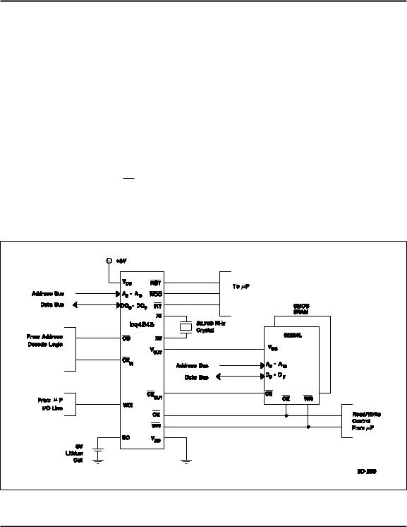
Figure 2 shows the hardware hookup for the external RAM, battery, and crystal.
A primary backup energy source input is provided on the bq4845. The BC input accepts a 3V primary battery, typically some type of lithium chemistry. Since the bq4845 provides for reverse battery charging protection, no diode or current limiting resistor is needed in series with the cell. To prevent battery drain when there is no valid data to retain, VOUT and CEOUT are internally isolated from BC by the initial connection of a battery. Following the first application of VCC above VPFD, this isolation is broken, and the backup cell provides power to VOUT and CEOUT for the external SRAM.
The crystal should be located as close to X1 and X2 as possible and meet the specifications in the Crystal Specification Table. With the specified crystal, the bq4845 RTC will be accurate to within one minute per month at room temperature. In the absence of a crystal, a 32.768 kHz waveform can be fed into X1 with X2 grounded.
Power-On Reset
The bq4845 provides a power-on reset, which pulls the RST pin low on power-down and remains low on powerup for tRST after VCC passes VPFD. With valid battery voltage on BC, RST remains valid for VCC= VSS.
Figure 2. bq4845 Application Circuit
Aug. 1995
6
 Loading...