


5962-8868505PA
Texas Instruments 5962-8868505PA, 5962-8868505HA, 5962-88685052A, 5962-8868504HA, 5962-88685042A Datasheet
...
TL7702B, TL7705B
SUPPLY-VOLTAGE SUPERVISORS
SLVS037H – SEPTEMBER 1989 – REVISED JULY 1999
1
POST OFFICE BOX 655303 • DALLAS, TEXAS 75265
D
Power-On Reset Generator
D
Automatic Reset Generation After
Voltage Drop
D
RESET Output Defined From VCC ≥ 1 V
D
Precision V oltage Sensor
D
T emperature-Compensated Voltage
Reference
D
True and Complement Reset Outputs
D
Externally Adjustable Pulse Duration
description
The TL7702B and TL7705B are integrated-circuit
supply-voltage supervisors designed for use as
reset controllers in microcomputer and
microprocessor systems. The supply-voltage
supervisor monitors the supply for undervoltage
conditions at the SENSE input. During power up,
the RESET
output becomes active (low) when
V
CC
attains a value approaching 1 V. As V
CC
approaches 3 V (assuming that SENSE is above
VT+), the delay timer function activates a time
delay , after which outputs RESET and RESET go
inactive (high and low, respectively). When an
undervoltage condition occurs during normal
operation, outputs RESET
and RESET go active.
To ensure that a complete reset occurs, the reset
outputs remain active for a time delay after the
voltage at the SENSE input exceeds the
positive-going threshold value. The time delay is
determined by the value of the external capacitor
C
T
: td ≈ 2.6 × 10⁴ × CT, where CT is in farads (F)
and td is in seconds (s).
An external capacitor (typically 0.1 µF) must be
connected to REF to reduce the influence of fast
transients in the supply voltage.
The TL7702BC and TL7705BC are characterized for operation from 0°C to 70°C. The TL7702BI and TL7705BI
are characterized for operation from –40°C to 85°C. The TL7705BQ is characterized for operation from –40°C
to 125°C. The TL7705BM is characterized for operation from –55°C to 125°C.
Please be aware that an important notice concerning availability, standard warranty, and use in critical applications of
Texas Instruments semiconductor products and disclaimers thereto appears at the end of this data sheet.
Copyright 1999, Texas Instruments Incorporated
PRODUCTION DATA information is current as of publication date.
Products conform to specifications per the terms of Texas Instruments
standard warranty. Production processing does not necessarily include
testing of all parameters.
3212019
910111213
4
5
6
7
8
18
17
16
15
14
NC
SENSE
NC
RESET
NC
NC
RESIN
NC
CT
NC
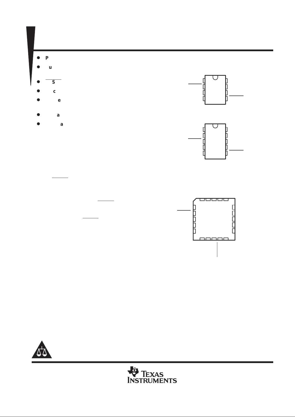
TL7705BM ...FK PACKAGE
(TOP VIEW)
NC
REF
NC
RESET
NC
V
NC
NC
GND
NC
CC
1
2
3
4
8
7
6
5
REF
RESIN
CT
GND
V
CC
SENSE
RESET
RESET
TL77xxBC ...D OR P PACKAGE
TL7705BM . . .JG PACKAGE
TL7705BQ ...D PACKAGE
(TOP VIEW)
1
2
3
4
5
10
9
8
7
6
NC
REF
RESIN
CT
GND
NC
V
CC
SENSE
RESET
RESET
TL7705BM ...U PACKAGE
(TOP VIEW)
•
NC – No internal connection
NC – No internal connection
On products compliant to MIL-PRF-38535, all parameters are tested
unless otherwise noted. On all other products, production
processing does not necessarily include testing of all parameters.
TL7702B, TL7705B
SUPPLY-VOLTAGE SUPER VISORS
SLVS037H – SEPTEMBER 1989 – REVISED JULY 1999
2
POST OFFICE BOX 655303 • DALLAS, TEXAS 75265
AVAILABLE OPTIONS
PACKAGED DEVICES
T
A
SMALL
OUTLINE
(D)
CHIP
CARRIER
(FK)
CERAMIC
DIP
(JG)
PLASTIC
DIP
(P)
CERAMIC
FLATPACK
(U)
CHIP FORM
(Y)
°
°
TL7702BCD — — TL7702BCP —
0°C to 70°C
TL7705BCD — — TL7705BCP —
°
°
TL7702BID — — TL7702BIP —
TL7702BY
,
–
40°C to 85°C
TL7705BID — — TL7705BIP —
TL7702BY,
TL7705BY
–40°C to 125°C TL7705BQD — — — —
°
°
— TL7702BMFK TL7702BMJG — TL7702BMU
–
55°C to 125°C
— TL7705BMFK TL7705BMJG — TL7705BMU
The D package is available taped and reeled. Add the suffix R to device type (e.g., TL7702BCDR). Chip forms are tested at
25°C.
TL7702B, TL7705B
SUPPLY-VOLTAGE SUPER VISORS
SLVS037H – SEPTEMBER 1989 – REVISED JULY 1999
3
POST OFFICE BOX 655303 • DALLAS, TEXAS 75265
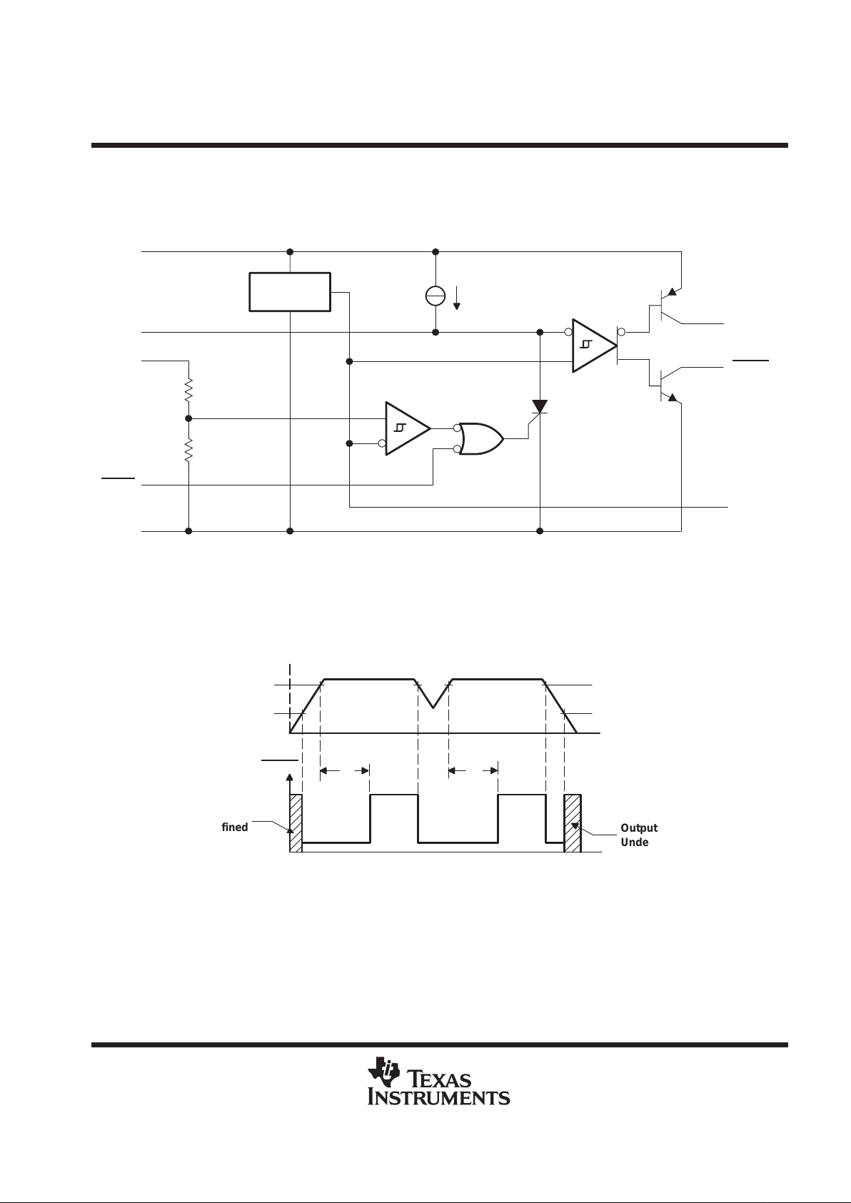
functional block diagram
The functional block diagram is shown for illustrative purposes only; the actual circuit includes a trimming
network to adjust the reference voltage and sense-comparator trip point.
RESIN
≈ 70 µA
R1
(see Note A)
R2
(see Note A)
Reference
Voltage
SENSE
GND
V
CC
CT
RESET
RESET
REF
8
3
7
2
4
6
5
1
Pin numbers shown are for the D, JG, and P packages.
NOTE A: TL7702B: R1 = 0 Ω, R2 = open
TL7705B: R1 = 23 kΩ, R2 = 10 kΩ, nominal
typical timing diagram
V
IT–
RESET
V
res
0
t
d
0
VCC and
SENSE
t
d
V
IT–
V
IT+
V
IT+
V
res
Output
Undefined
Output
Undefined
TL7702B, TL7705B
SUPPLY-VOLTAGE SUPER VISORS
SLVS037H – SEPTEMBER 1989 – REVISED JULY 1999
4
POST OFFICE BOX 655303 • DALLAS, TEXAS 75265
absolute maximum ratings over operating free-air temperature range (unless otherwise noted)
†
Supply voltage, VCC (see Note 1) 20 V. . . . . . . . . . . . . . . . . . . . . . . . . . . . . . . . . . . . . . . . . . . . . . . . . . . . . . . . . . . .
Input voltage range, VI: RESIN –0.3 V to 20 V. . . . . . . . . . . . . . . . . . . . . . . . . . . . . . . . . . . . . . . . . . . . . . . . . . . . .
SENSE –0.3 V to 20 V. . . . . . . . . . . . . . . . . . . . . . . . . . . . . . . . . . . . . . . . . . . . . . . . . . . .
High-level output current, I
OH
(RESET) –30 mA. . . . . . . . . . . . . . . . . . . . . . . . . . . . . . . . . . . . . . . . . . . . . . . . . . . .
Low-level output current, IOL (RESET) 30 mA. . . . . . . . . . . . . . . . . . . . . . . . . . . . . . . . . . . . . . . . . . . . . . . . . . . . . .
Package thermal impedance, θJA (see Notes 2 and 3): D package 97°C/W. . . . . . . . . . . . . . . . . . . . . . . . . . . .
P package 127°C/W. . . . . . . . . . . . . . . . . . . . . . . . . . . .
Case temperature for 60 seconds, T
C
: FK package 260°C. . . . . . . . . . . . . . . . . . . . . . . . . . . . . . . . . . . . . . . . . .
Lead temperature 1,6 mm (1/16 inch) from case for 60 seconds: JG or U packages 300°C. . . . . . . . . . . . . .
Lead temperature 1,6 mm (1/16 inch) from case for 10 seconds: D or P packages 260°C. . . . . . . . . . . . . . . .
Storage temperature range, T
stg
–65°C to 150°C. . . . . . . . . . . . . . . . . . . . . . . . . . . . . . . . . . . . . . . . . . . . . . . . . .
†
Stresses beyond those listed under “absolute maximum ratings” may cause permanent damage to the device. These are stress ratings only, and
functional operation of the device at these or any other conditions beyond those indicated under “recommended operating conditions” is not
implied. Exposure to absolute-maximum-rated conditions for extended periods may affect device reliability.
NOTES: 1. All voltage values are with respect to the network ground terminal.
2. Maximum power dissipation is a function of TJ(max),
θ
JA
, and TA. The maximum allowable power dissipation at any allowable
ambient temperature is PD = (TJ(max) – TA)/
θ
JA
. Operating at the absolute maximum TJ of 150°C can impact reliability.
3. The package thermal impedance is calculated in accordance with JESD 51, except for through-hole packages, which use a trace
length of zero.
recommended operating conditions
MIN MAX UNIT
Supply voltage, V
CC
3.6 18 V
High-level input voltage, V
IH
RESIN 2 18 V
Low-level input voltage, V
IL
RESIN 0 0.8 V
Input voltage, V
I
SENSE 0 18 V
High-level output current, I
OH
RESET –16 mA
Low-level output current, I
OL
RESET 16 mA
TL770xBC 0 70
p
p
TL770xBI –40 85
°
Operating free-air temperature range, T
A
TL7705BQ –40 125
°C
TL7705BM –55 125
 Loading...