


|
|
|
|
|
|
|
|
|
|
|
|
|
|
|
|
|
|
|
|
|
TLC225x, TLC225xA |
||||||||||||||||||
|
|
|
|
|
|
|
|
|
|
|
Advanced LinCMOS |
|
RAIL-TO-RAIL |
||||||||||||||||||||||||||
|
|
|
|
|
|
|
|
VERY LOW-POWER OPERATIONAL AMPLIFIERS |
|||||||||||||||||||||||||||||||
|
|
|
|
|
|
|
|
|
|
|
|
SLOS176A ± FEBRUARY 1997 ± REVISED JULY 1999 |
|||||||||||||||||||||||||||
|
|
|
|
|
|
|
|
|
|
|
|
|
|
|
|
|
|
|
|
|
|
|
|
|
|
|
|
|
|
|
|
|
|
|
|||||
D Output Swing Includes Both Supply Rails |
D Low Input Offset Voltage |
|
|
|
|
|
|
|
|
|
|
|
|
|
|||||||||||||||||||||||||
D Low Noise . . . 19 nV/√ |
|
Typ at f = 1 kHz |
|
|
850 V Max at TA = 25°C (TLC225xA) |
|
|
|
|
|
|||||||||||||||||||||||||||||
Hz |
|
|
|
|
|
|
|
||||||||||||||||||||||||||||||||
D Low Input Bias Current . . . 1 pA Typ |
|
D |
Macromodel Included |
|
|
|
|
|
|
|
|
|
|
|
|
|
|||||||||||||||||||||||
D Fully Specified for Both Single-Supply and |
D Performance Upgrades for the TS27L2/L4 |
|
|
|
|
|
|||||||||||||||||||||||||||||||||
|
and TLC27L2/L4 |
|
|
|
|
|
|
|
|
|
|
|
|
|
|||||||||||||||||||||||||
Split-Supply Operation |
|
|
|
|
|
|
|
|
|
|
|
|
|
|
|
|
|
|
|||||||||||||||||||||
|
|
|
|
|
|
|
|
|
|
|
|
|
|
|
|
|
|
|
|
|
|
|
|
|
|
|
|
|
|
|
|
|
|
|
|||||
D Very Low Power . . . 35 A Per Channel Typ |
D Available in Q±Temp Automotive |
|
|
|
|
|
|||||||||||||||||||||||||||||||||
D Common-Mode Input Voltage Range |
|
|
HighRel Automotive Applications |
|
|
|
|
|
|||||||||||||||||||||||||||||||
|
|
Configuration Control / Print Support |
|
|
|
|
|
||||||||||||||||||||||||||||||||
Includes Negative Rail |
|
|
|
|
|
|
|
|
|
|
|||||||||||||||||||||||||||||
|
|
|
|
|
Qualification to Automotive Standards |
|
|
|
|
|
|||||||||||||||||||||||||||||
|
|
|
|
|
|
|
|
|
|
|
|
|
|
|
|||||||||||||||||||||||||
description |
|
|
|
|
|
|
|
|
|
|
EQUIVALENT INPUT NOISE VOLTAGE |
|
|
|
|
|
|||||||||||||||||||||||
The TLC2252 |
and TLC2254 are dual |
and |
|
|
|
|
|
|
|
|
|
|
|
|
vs |
|
|
|
|
|
|
|
|
|
|
|
|
|
|||||||||||
|
|
|
|
|
|
|
|
|
|
|
FREQUENCY |
|
|
|
|
|
|||||||||||||||||||||||
quadruple operational amplifiers from Texas |
|
|
|
|
|
|
|
|
|
|
|
|
|
|
|
|
|||||||||||||||||||||||
|
60 |
|
|
|
|
|
|
|
|
|
|
|
|
|
|
|
|
|
|
|
|
|
|
|
|
|
|
|
|
|
|||||||||
Instruments. |
Both devices |
exhibit rail-to-rail |
Hz |
|
VDD = 5 V |
|
|
|
|
|
|
|
|
|
|
|
|
|
|
|
|
|
|
|
|
|
|
|
|
||||||||||
output performance for increased dynamic range |
|
RS = 20 Ω |
|
|
|
|
|
|
|
|
|
|
|
|
|
|
|
|
|
|
|
|
|
|
|
|
|||||||||||||
nV/nv//Hz |
|
|
|
|
|
|
|
|
|
|
|
|
|
|
|
|
|
|
|
|
|
|
|
|
|
||||||||||||||
in single- |
or |
split-supply |
applications. |
The |
50 |
TA = 25°C |
|
|
|
|
|
|
|
|
|
|
|
|
|
|
|
|
|
|
|
|
|
|
|
|
|
||||||||
|
|
|
|
|
|
|
|
|
|
|
|
|
|
|
|
|
|
|
|
|
|
|
|
|
|||||||||||||||
|
|
|
|
|
|
|
|
|
|
|
|
|
|
|
|
|
|
|
|
|
|
|
|
|
|
|
|
|
|||||||||||
TLC225x family consumes only 35 A of supply |
|
|
|
|
|
|
|
|
|
|
|
|
|
|
|
|
|
|
|
|
|
|
|
|
|
|
|
|
|
|
|||||||||
± |
|
|
|
|
|
|
|
|
|
|
|
|
|
|
|
|
|
|
|
|
|
|
|
|
|
|
|
|
|
|
|||||||||
Voltage |
|
|
|
|
|
|
|
|
|
|
|
|
|
|
|
|
|
|
|
|
|
|
|
|
|
|
|
|
|
|
|||||||||
current per channel. This micropower operation |
40 |
|
|
|
|
|
|
|
|
|
|
|
|
|
|
|
|
|
|
|
|
|
|
|
|
|
|
|
|
|
|||||||||
makes them good choices for battery-powered |
|
|
|
|
|
|
|
|
|
|
|
|
|
|
|
|
|
|
|
|
|
|
|
|
|
|
|
|
|
||||||||||
|
|
|
|
|
|
|
|
|
|
|
|
|
|
|
|
|
|
|
|
|
|
|
|
|
|
|
|
|
|
||||||||||
applications. The noise performance has been |
|
|
|
|
|
|
|
|
|
|
|
|
|
|
|
|
|
|
|
|
|
|
|
|
|
|
|
|
|
|
|||||||||
Noise |
|
|
|
|
|
|
|
|
|
|
|
|
|
|
|
|
|
|
|
|
|
|
|
|
|
|
|
|
|
|
|||||||||
dramatically improved over previous generations |
30 |
|
|
|
|
|
|
|
|
|
|
|
|
|
|
|
|
|
|
|
|
|
|
|
|
|
|
|
|
|
|||||||||
|
|
|
|
|
|
|
|
|
|
|
|
|
|
|
|
|
|
|
|
|
|
|
|
|
|
|
|
|
|||||||||||
of CMOS amplifiers. Looking at Figure 1, the |
Input |
|
|
|
|
|
|
|
|
|
|
|
|
|
|
|
|
|
|
|
|
|
|
|
|
|
|
|
|
|
|
||||||||
TLC225x has a noise level of 19 nV/√ |
Hz |
at 1kHz; |
|
|
|
|
|
|
|
|
|
|
|
|
|
|
|
|
|
|
|
|
|
|
|
|
|
|
|
|
|
|
|||||||
four times lower than competitive micropower |
± Equivalent |
20 |
|
|
|
|
|
|
|
|
|
|
|
|
|
|
|
|
|
|
|
|
|
|
|
|
|
|
|
|
|
||||||||
|
|
|
|
|
|
|
|
|
|
|
|
|
|
|
|
|
|
|
|
|
|
|
|
|
|
|
|
|
|||||||||||
solutions. |
|
|
|
|
|
|
|
|
|
|
|
|
|
|
|
|
|
|
|
|
|
|
|
|
|
|
|
|
|
|
|
|
|
|
|
|
|
|
|
The TLC225x amplifiers, exhibiting high input |
10 |
|
|
|
|
|
|
|
|
|
|
|
|
|
|
|
|
|
|
|
|
|
|
|
|
|
|
|
|
|
|||||||||
|
|
|
|
|
|
|
|
|
|
|
|
|
|
|
|
|
|
|
|
|
|
|
|
|
|
|
|
|
|||||||||||
impedance |
and |
low noise, |
are excellent |
for |
|
|
|
|
|
|
|
|
|
|
|
|
|
|
|
|
|
|
|
|
|
|
|
|
|
|
|
|
|
|
|||||
n |
|
|
|
|
|
|
|
|
|
|
|
|
|
|
|
|
|
|
|
|
|
|
|
|
|
|
|
|
|
|
|||||||||
small-signal |
conditioning for high-impedance |
|
|
|
|
|
|
|
|
|
|
|
|
|
|
|
|
|
|
|
|
|
|
|
|
|
|
|
|
|
|
||||||||
VN |
0 |
|
|
|
|
|
|
|
|
|
|
|
|
|
|
|
|
|
|
|
|
|
|
|
|
|
|
|
|
|
|||||||||
sources, such as piezoelectric transducers. |
|
|
|
|
|
|
|
|
|
|
|
|
|
|
|
|
|
|
|
|
|
|
|
|
|
|
|
|
|
|
|||||||||
|
101 |
|
|
|
|
|
10 2 |
|
|
|
|
|
|
10 3 |
|
|
|
|
|
10 4 |
|
||||||||||||||||||
Because of |
the |
micropower |
dissipation levels, |
|
|
|
|
|
|
|
|
|
f ± Frequency ± Hz |
|
|
|
|
|
|||||||||||||||||||||
these devices work well in hand-held monitoring |
|
|
|
|
|
|
|
|
|
|
|
|
|
|
|||||||||||||||||||||||||
|
|
|
|
|
|
|
|
|
|
Figure 1 |
|
|
|
|
|
|
|
|
|
|
|
|
|
||||||||||||||||
and remote-sensing applications. In addition, the |
|
|
|
|
|
|
|
|
|
|
|
|
|
|
|
|
|
|
|
|
|
|
|
||||||||||||||||
rail-to-rail output feature with single or |
split |
|
|
|
|
|
|
|
|
|
|
|
|
|
|
|
|
|
|
|
|
|
|
|
|
|
|
|
|
|
|
|
|||||||
supplies makes this family a great choice when interfacing with analog-to-digital converters (ADCs). For precision applications, the TLC225xA family is available and has a maximum input offset voltage of 850 V. This family is fully characterized at 5 V and ± 5 V.
The TLC2252/4 also makes great upgrades to the TLC27L2/L4 or TS27L2/L4 in standard designs. They offer increased output dynamic range, lower noise voltage, and lower input offset voltage. This enhanced feature set allows them to be used in a wider range of applications. For applications that require higher output drive and wider input voltage ranges, see the TLV2432 and TLV2442 devices. If the design requires single amplifiers, please see the TLV2211/21/31 family. These devices are single rail-to-rail operational amplifiers in the SOT-23 package. Their small size and low power consumption, make them ideal for high density, battery-powered equipment.
Please be aware that an important notice concerning availability, standard warranty, and use in critical applications of Texas Instruments semiconductor products and disclaimers thereto appears at the end of this data sheet.
Advanced LinCMOS is a trademark of Texas Instruments Incorporated.
PRODUCTION DATA information is current as of publication date. Products conform to specifications per the terms of Texas Instruments standard warranty. Production processing does not necessarily include testing of all parameters.
Copyright 1999, Texas Instruments Incorporated
On products compliant to MIL-PRF-38535, all parameters are tested unless otherwise noted. On all other products, production processing does not necessarily include testing of all parameters.
POST OFFICE BOX 655303 •DALLAS, TEXAS 75265 |
1 |
TLC225x, TLC225xA
Advanced LinCMOS RAIL-TO-RAIL
VERY LOW-POWER OPERATIONAL AMPLIFIERS
SLOS176A ± FEBRUARY 1997 ± REVISED JULY 1999
TLC2252 AVAILABLE OPTIONS
|
|
|
|
|
|
|
|
|
|
|
|
|
PACKAGED DEVICES |
|
|
|
|
|
|||
|
|
|
|
VIOmax |
|
|
|
|
|
|
|
|
|
|
|
|
|
|
|
|
|
TA |
|
|
|
SMALL |
|
|
CHIP |
|
CERAMIC |
PLASTIC |
|
TSSOP³ |
|
CERAMIC |
|||||||
|
|
AT 25°C |
OUTLINE² |
|
|
CARRIER |
DIP |
|
DIP |
|
|
FLATPACK |
|||||||||
|
|
|
|
|
|
|
|
(PW) |
|
||||||||||||
|
|
|
|
|
|
(D) |
|
|
(FK) |
|
(JG) |
|
(P) |
|
|
(U) |
|||||
|
|
|
|
|
|
|
|
|
|
|
|
|
|
||||||||
|
|
|
|
|
|
|
|
|
|
|
|
|
|
|
|
|
|
|
|||
0°C to 70°C |
|
1500 V |
TLC2252CD |
|
|
Ð |
|
|
Ð |
|
TLC2252CP |
TLC2252CPWLE |
|
Ð |
|||||||
|
|
|
|
|
|
|
|
|
|
|
|
|
|
|
|
|
|
|
|
||
±40°C to 85°C |
|
850 V |
TLC2252AID |
|
|
Ð |
|
|
Ð |
|
TLC2252AIP |
TLC2252AIPWLE |
|
Ð |
|||||||
|
1500 V |
TLC2252ID |
|
|
Ð |
|
|
Ð |
|
TLC2252IP |
|
Ð |
|
|
Ð |
||||||
|
|
|
|
|
|
|
|
|
|
|
|
||||||||||
|
|
|
|
|
|
|
|
|
|
|
|
|
|
|
|
|
|
|
|
||
±40°C to 125°C |
|
850 V |
TLC2252AQD |
|
Ð |
|
|
Ð |
|
Ð |
|
|
Ð |
|
|
Ð |
|||||
|
1500 V |
TLC2252QD |
|
|
Ð |
|
|
Ð |
|
Ð |
|
|
Ð |
|
|
Ð |
|||||
|
|
|
|
|
|
|
|
|
|
|
|
|
|||||||||
|
|
|
|
|
|
|
|
|
|
|
|
|
|
|
|
|
|
|
|
|
|
± 55°C to 125°C |
|
850 V |
|
Ð |
|
|
TLC2252AMFK |
TLC2252AMJG |
Ð |
|
|
Ð |
|
|
TLC2252AMU |
||||||
|
1500 V |
|
Ð |
|
|
TLC2252MFK |
TLC2252MJG |
Ð |
|
|
Ð |
|
|
TLC2252MU |
|||||||
|
|
|
|
|
|
|
|
|
|
|
|||||||||||
² The D packages are available taped and reeled. Add R suffix to device type (e.g., TLC2262CDR). |
|
|
|
|
|
||||||||||||||||
³ The PW package is available only left-ended taped and reeled. |
|
|
|
|
|
|
|
|
|
|
|||||||||||
§ Chip forms are tested at 25°C only. |
|
|
|
|
|
|
|
|
|
|
|
|
|
|
|
|
|
||||
|
|
|
|
|
|
|
|
|
|
TLC2254 AVAILABLE OPTIONS |
|
|
|
|
|
|
|
||||
|
|
|
|
|
|
|
|
|
|
|
|
|
|
|
|
|
|
|
|
|
|
|
|
|
|
|
|
|
|
|
|
|
|
|
PACKAGED DEVICES |
|
|
|
|
|
|||
|
|
VIOmax |
|
|
|
|
|
|
|
|
|
|
|
|
|
|
|
||||
TA |
|
|
SMALL |
|
|
CHIP |
|
CERAMIC |
PLASTIC DIP |
|
|
TSSOP³ |
|
|
CERAMIC |
||||||
|
AT 25°C |
|
OUTLINE² |
|
CARRIER |
|
|
DIP |
|
|
|
|
FLATPACK |
||||||||
|
|
|
|
|
|
|
(N) |
|
|
(PW) |
|
|
|||||||||
|
|
|
|
(D) |
|
|
|
|
(FK) |
|
|
(J) |
|
|
|
|
|
(W) |
|||
|
|
|
|
|
|
|
|
|
|
|
|
|
|
|
|
|
|||||
|
|
|
|
|
|
|
|
|
|
|
|
|
|
|
|
|
|
|
|
|
|
0°C to |
|
1500 V |
|
TLC2254CD |
|
|
|
Ð |
|
|
Ð |
TLC2254CN |
|
TLC2254CPWLE |
|
Ð |
|||||
70°C |
|
|
|
|
|
|
|
|
|
||||||||||||
|
|
|
|
|
|
|
|
|
|
|
|
|
|
|
|
|
|
|
|
|
|
|
|
|
|
|
|
|
|
|
|
|
|
|
|
|
|
|
|||||
± 40°C to |
|
850 V |
|
TLC2254AID |
|
|
|
Ð |
|
|
Ð |
TLC2254AIN |
|
TLC2254AIPWLE |
|
Ð |
|||||
85°C |
|
1500 V |
|
TLC2254ID |
|
|
|
Ð |
|
|
Ð |
TLC2254IN |
|
|
Ð |
|
Ð |
||||
|
|
|
|
|
|
|
|
|
|
|
|
|
|
|
|
|
|
||||
± 40°C to |
|
850 V |
|
TLC2254AQD |
|
|
Ð |
|
|
Ð |
|
Ð |
|
|
Ð |
|
Ð |
||||
125°C |
|
1500 V |
|
TLC2254QD |
|
|
|
Ð |
|
|
Ð |
|
Ð |
|
|
Ð |
|
Ð |
|||
|
|
|
|
|
|
|
|
|
|
|
|
|
|
|
|
|
|||||
± 55°C to |
|
850 V |
|
Ð |
|
|
TLC2254AMFK |
|
TLC2254AMJ |
|
Ð |
|
|
Ð |
|
TLC2254AMW |
|||||
125°C |
|
1500 V |
|
Ð |
|
|
TLC2254MFK |
|
TLC2254MJ |
|
Ð |
|
|
Ð |
|
TLC2254MW |
|||||
|
|
|
|
|
|
|
|
|
|
|
|
|
|
|
|
|
|
|
|
|
|
² The D packages are available taped and reeled. Add R suffix to the device type (e.g., TLC2254CDR). ³ The PW package is available only left-end taped and reeled. Chips are tested at 25°C.
§ Chip forms are tested at 25°C only.
2 |
POST OFFICE BOX 655303 •DALLAS, TEXAS 75265 |
|
|
|
|
|
|
|
|
|
TLC225x, TLC225xA |
|
|
|
|
Advanced LinCMOS RAIL-TO-RAIL |
|||||
|
|
|
|
VERY LOW-POWER OPERATIONAL AMPLIFIERS |
|||||
|
|
|
|
|
SLOS176A ± FEBRUARY 1997 ± REVISED JULY 1999 |
||||
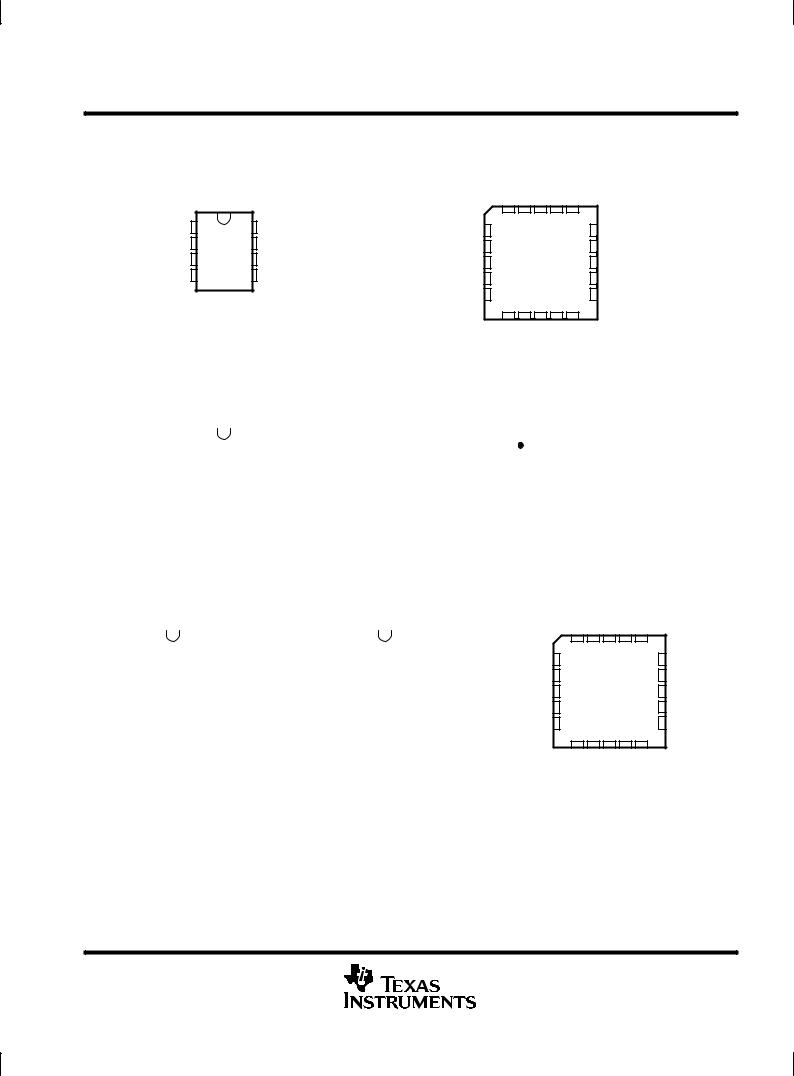
TLC2252C, TLC2252AC |
TLC2252M, TLC2252AM . . . FK PACKAGE |
||||||||
TLC2252I, TLC2252AI |
|
|
(TOP VIEW) |
|
|||||
TLC2252Q, TLC2252AQ |
|
|
1OUT |
|
DD+ |
|
|||
D, P, OR PW PACKAGE |
|
NC |
NC |
|
|||||
|
V NC |
|
|||||||
|
(TOP VIEW) |
|
|
|
|
|
|
|
|
1OUT |
1 |
8 |
VDD + |
NC |
3 |
2 |
1 |
20 19 |
NC |
4 |
|
|
18 |
||||||
1IN ± |
2 |
7 |
2OUT |
1IN ± |
5 |
|
|
17 |
2OUT |
1IN + |
3 |
6 |
2IN ± |
NC |
6 |
|
|
16 |
NC |
VDD ±/GND |
4 |
5 |
2IN + |
1IN + |
7 |
|
|
15 |
2IN ± |
|
|
|
|
NC |
8 |
|
|
14 |
NC |
|
|
|
|
|
9 |
10 11 12 13 |
|
||
|
|
|
|
|
NC |
/GND |
NC |
2IN+ NC |
|
|
|
|
|
|
|
DD± |
|
|
|
|
|
|
|
|
|
V |
|
|
|
TLC2252M, TLC2252AM . . . JG PACKAGE |
TLC2262M, TLC2252AM . . . U PACKAGE |
||||||||
|
(TOP VIEW) |
|
|
|
(TOP VIEW) |
|
|||
1OUT |
|
1 |
8 |
|
VDD + |
NC |
|
1 |
10 |
|
NC |
|
|
|
|
||||||||
1IN ± |
|
2 |
7 |
|
2OUT |
1OUT |
|
2 |
9 |
|
VCC + |
|
|
|
|
||||||||
1IN + |
|
3 |
6 |
|
2IN ± |
1IN ± |
|
3 |
8 |
|
2OUT |
VDD ±/GND |
|
4 |
5 |
|
2IN + |
1IN + |
|
4 |
7 |
|
2IN ± |
|
|
|
|
|
|
VCC ±/GND |
|
5 |
6 |
|
2IN + |
|
|
|
|
|
|
|
|
||||
|
|
|
|
|
|
|
|
TLC2254C, TLC2254AC |
|
TLC2254I, TLC2254AI |
|
TLC2254Q, TLC2254AQ |
TLC2254M, TLC2254AM |
D, N, OR PW PACKAGE |
J OR W PACKAGE |
(TOP VIEW) |
(TOP VIEW) |
1OUT |
|
1 |
14 |
|
4OUT |
1OUT |
|
1 |
14 |
|
4OUT |
|
|
|
|
||||||||
1IN ± |
|
2 |
13 |
|
4IN ± |
1IN± |
|
2 |
13 |
|
4IN± |
|
|
|
|
||||||||
1IN + |
|
3 |
12 |
|
4IN + |
1IN+ |
|
3 |
12 |
|
4IN+ |
|
|
|
|
||||||||
VDD + |
|
4 |
11 |
|
VDD ±/ GND |
VDD + |
|
4 |
11 |
|
VDD ±/GND |
|
|
|
|
||||||||
|
|
|
|
||||||||
2IN + |
|
5 |
10 |
|
3IN + |
2IN+ |
|
5 |
10 |
|
3IN+ |
|
|
|
|
3IN ± |
|
|
|
|
|
3IN± |
|
2IN ± |
|
6 |
9 |
|
2IN± |
|
6 |
9 |
|
||
|
|
|
|
3OUT |
|
|
|
|
|
3OUT |
|
2OUT |
|
7 |
8 |
|
2OUT |
|
7 |
8 |
|
||
|
|
|
|
|
|
|
|
|
|
|
|
TLC2254M, TLC2254AM
FK PACKAGE
(TOP VIEW)
|
1IN ± |
1OUT |
NC |
4OUT |
4IN ± |
|
1IN + |
3 |
2 |
1 |
20 19 |
4IN + |
|
4 |
|
|
|
18 |
||
NC |
5 |
|
|
|
17 |
NC |
VCC + |
6 |
|
|
|
16 |
VCC ±/GND |
NC |
7 |
|
|
|
15 |
NC |
2IN + |
8 |
|
|
|
14 |
3IN + |
|
9 |
10 11 12 13 |
|
|||
|
2IN ± |
2OUT |
NC |
3OUT |
3IN ± |
|
POST OFFICE BOX 655303 •DALLAS, TEXAS 75265 |
3 |
4
75265 TEXAS DALLAS, •655303 BOX OFFICE POST
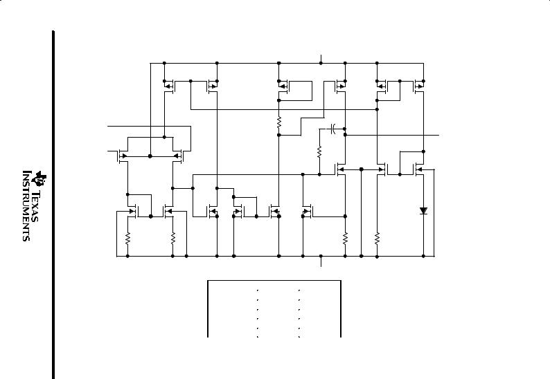
equivalent schematic (each amplifier) |
|
|
|
|
|
||
|
|
|
|
|
VDD + |
|
|
|
Q3 |
Q6 |
|
Q9 |
Q12 |
Q14 |
Q16 |
IN + |
|
|
|
R6 |
|
|
|
|
|
|
|
|
|
|
|
|
|
|
|
|
C1 |
|
OUT |
|
|
|
|
|
|
|
|
IN ± |
|
|
|
|
R5 |
|
|
|
|
|
|
|
|
|
|
Q1 |
|
Q4 |
|
|
|
|
|
|
|
|
|
|
Q13 |
Q15 |
Q17 |
|
|
|
|
|
|
|
D1 |
Q2 |
Q5 |
Q7 |
Q8 |
Q10 |
Q11 |
|
|
R3 |
R4 |
|
|
|
R1 |
R2 |
|
|
|
|
|
|
VDD ± / GND |
|
|
ACTUAL DEVICE COMPONENT COUNT²
COMPONENT |
TLC2252 |
TLC2254 |
|
|
|
Transistors |
38 |
76 |
|
|
|
Resistors |
30 |
56 |
|
|
|
Diodes |
9 |
18 |
|
|
|
Capacitors |
3 |
6 |
²Includes both amplifiers and all ESD, bias, and trim circuitry
1999 JULY REVISED ± 1997 FEBRUARY ± SLOS176A
TLC225xA TLC225x, RAIL-TO-RAIL LinCMOS Advanced AMPLIFIERS OPERATIONAL POWER-LOW VERY |
7±11±94 Date: Release Template |

TLC225x, TLC225xA
Advanced LinCMOS RAIL-TO-RAIL
VERY LOW-POWER OPERATIONAL AMPLIFIERS
SLOS176A ± FEBRUARY 1997 ± REVISED JULY 1999
absolute maximum ratings over operating free-air temperature range (unless otherwise noted)²
Supply voltage, VDD + (see Note 1) . . . . . . . . . . . . . . . . . . . . . . . . . . . . . . . . . . . . . . |
. . . . . . . . . . . . . . . . . . . . . . 8 V |
Supply voltage, VDD ± (see Note 1) . . . . . . . . . . . . . . . . . . . . . . . . . . . . . . . . . . . . . . |
. . . . . . . . . . . . . . . . . . . . . ±8 V |
Differential input voltage, VID (see Note 2) . . . . . . . . . . . . . . . . . . . . . . . . . . . . . . . |
. . . . . . . . . . . . . . . . . . . . ± 16 V |
Input voltage, VI (any input, see Note 1) . . . . . . . . . . . . . . . . . . . . . . . . . . . . . . . . . |
. . . . . . . . . . . . . . . . . . . . . ± 8 V |
Input current, II (each input) . . . . . . . . . . . . . . . . . . . . . . . . . . . . . . . . . . . . . . . . . . . . |
. . . . . . . . . . . . . . . . . . . ± 5 mA |
Output current, IO . . . . . . . . . . . . . . . . . . . . . . . . . . . . . . . . . . . . . . . . . . . . . . . . . . . . . |
. . . . . . . . . . . . . . . . . . ± 50 mA |
Total current into VDD + . . . . . . . . . . . . . . . . . . . . . . . . . . . . . . . . . . . . . . . . . . . . . . . . |
. . . . . . . . . . . . . . . . . . ± 50 mA |
Total current out of VDD ± . . . . . . . . . . . . . . . . . . . . . . . . . . . . . . . . . . . . . . . . . . . . . . |
. . . . . . . . . . . . . . . . . . ± 50 mA |
Duration of short-circuit current at (or below) 25°C (see Note 3) . . . . . . . . . . . . . |
. . . . . . . . . . . . . . . . . unlimited |
Continuous total dissipation . . . . . . . . . . . . . . . . . . . . . . . . . . . . . . . . . . . . . . . . . . . |
See Dissipation Rating Table |
Operating free-air temperature range, TA: C suffix . . . . . . . . . . . . . . . . . . . . . . . . |
. . . . . . . . . . . . . . 0°C to 70°C |
I suffix . . . . . . . . . . . . . . . . . . . . . . . . . |
. . . . . . . . . . . . ±40°C to 85°C |
Q suffix . . . . . . . . . . . . . . . . . . . . . . . . |
. . . . . . . . . . . ±40°C to 125°C |
M suffix . . . . . . . . . . . . . . . . . . . . . . . |
. . . . . . . . . . . ±55°C to 125°C |
Storage temperature range, Tstg . . . . . . . . . . . . . . . . . . . . . . . . . . . . . . . . . . . . . . . . |
. . . . . . . . . . . ±65°C to 150°C |
Lead temperature 1,6 mm (1/16 inch) from case for 10 seconds . . . . . . . . . . . . |
. . . . . . . . . . . . . . . . . . . 260°C |
²Stresses beyond those listed under ªabsolute maximum ratingsº may cause permanent damage to the device. These are stress ratings only, and functional operation of the device at these or any other conditions beyond those indicated under ªrecommended operating conditionsº is not
implied. Exposure to absolute-maximum-rated conditions for extended periods may affect device reliability.
NOTES: 1. All voltage values, except differential voltages, are with respect to the midpoint between VDD+ and VDD ±.
2. Differential voltages are at IN+ with respect to IN ±. Excessive current flows when input is brought below VDD ± ± 0.3 V.
3.The output may be shorted to either supply. Temperature and/or supply voltages must be limited to ensure that the maximum dissipation rating is not exceeded.
DISSIPATION RATING TABLE
PACKAGE |
TA ≤ 25°C |
DERATING FACTOR |
TA = 70°C |
TA = 85°C |
TA = 125°C |
|
POWER RATING |
ABOVE TA = 25°C |
POWER RATING |
POWER RATING |
POWER RATING |
||
|
||||||
D±8 |
724 mW |
5.8 mW/°C |
464 mW |
377 mW |
144 mW |
|
D±14 |
950 mW |
7.6 mW/°C |
608 mW |
450 mW |
190 mW |
|
FK |
1375 mW |
11.0 mW/°C |
880 mW |
715 mW |
275 mW |
|
J |
1375 mW |
11.0 mW/°C |
880 mW |
715 mW |
275 mW |
|
JG |
1050 mW |
8.4 mW/°C |
672 mW |
546 mW |
275 mW |
|
N |
1150 mW |
9.2 mW/°C |
736 mW |
736 mW |
Ð |
|
P |
1000 mW |
8.0 mW/°C |
640 mW |
520 mW |
Ð |
|
PW±8 |
525 mW |
4.2 mW/°C |
336 mW |
273 mW |
Ð |
|
PW±14 |
700 mW |
5.6 mW/°C |
448 mW |
448 mW |
Ð |
|
U |
700 mW |
5.5 mW/°C |
246 mW |
330 mW |
150 mW |
|
W |
700 mW |
5.5 mW/°C |
246 mW |
330 mW |
150 mW |
recommended operating conditions
|
C SUFFIX |
I SUFFIX |
Q SUFFIX |
M SUFFIX |
UNIT |
|
||||
|
|
|
|
|
|
|
|
|
|
|
|
MIN |
MAX |
MIN |
MAX |
MIN |
MAX |
MIN |
MAX |
|
|
|
|
|
||||||||
|
|
|
|
|
|
|
|
|
|
|
Supply voltage, VDD ± |
± 2.2 |
± 8 |
± 2.2 |
± 8 |
± 2.2 |
± 8 |
± 2.2 |
± 8 |
V |
|
Input voltage range, VI |
VDD ± |
VDD + ± 1.5 |
VDD ± |
VDD + ± 1.5 |
VDD ± |
VDD + ± 1.5 |
VDD ± |
VDD + ± 1.5 |
V |
|
Common-mode input voltage, VIC |
VDD ± |
VDD + ± 1.5 |
VDD ± |
VDD + ± 1.5 |
VDD ± |
VDD + ± 1.5 |
VDD ± |
VDD + ± 1.5 |
V |
|
Operating free-air temperature, TA |
0 |
70 |
± 40 |
85 |
± 40 |
125 |
± 55 |
125 |
°C |
|
|
|
|
|
|
|
|
|
|
|
|
|
|
|
|
|
|
|
|
|
|
|
POST OFFICE BOX 655303 •DALLAS, TEXAS 75265 |
5 |

TLC225x, TLC225xA
Advanced LinCMOS RAIL-TO-RAIL
VERY LOW-POWER OPERATIONAL AMPLIFIERS
SLOS176A ± FEBRUARY 1997 ± REVISED JULY 1999
electrical characteristics at specified free-air temperature, VDD = 5 V (unless otherwise noted)
|
PARAMETER |
TEST CONDITIONS |
T ² |
TLC2252C |
|
UNIT |
||
|
|
|
|
|||||
|
|
|
|
|||||
|
|
|
|
A |
MIN |
TYP |
MAX |
|
|
|
|
|
|
|
|||
VIO |
Input offset voltage |
|
|
25°C |
|
200 |
1500 |
µV |
|
|
|
|
|
|
|||
|
|
Full range |
|
|
1750 |
|||
|
|
|
|
|
|
|
||
|
|
|
|
|
|
|
|
|
αVIO |
Temperature coefficient of input offset voltage |
|
|
25°C |
|
0.5 |
|
µV/°C |
|
|
to 70°C |
|
|
||||
|
|
|
VDD ± = ± 2.5 V, |
|
|
|
|
|
|
|
VIC = 0, |
|
|
|
|
|
|
|
Input offset voltage long-term drift (see Note 4) |
25°C |
|
0.003 |
|
µV/mo |
||
|
|
VO = 0, |
RS = 50 Ω |
|
|
|
|
|
IIO |
Input offset current |
25°C |
|
0.5 |
|
pA |
||
|
|
|
|
|||||
|
|
Full range |
|
|
100 |
|||
|
|
|
|
|
|
|
||
|
|
|
|
|
|
|
|
|
IIB |
Input bias current |
|
|
25°C |
|
1 |
|
pA |
|
|
Full range |
|
|
100 |
|||
|
|
|
|
|
|
|
||
|
|
|
|
|
|
|
|
|
|
|
|
|
25°C |
0 |
± 0.3 |
|
|
|
|
|
|
to |
to |
|
|
|
VICR |
Common-mode input voltage range |
RS = 50 Ω, |
|VIO | ≤ 5 mV |
|
4 |
4.2 |
|
V |
|
|
|
|
|||||
|
0 |
|
|
|||||
|
|
|
|
|
|
|
|
|
|
|
|
|
Full range |
to |
|
|
|
|
|
|
|
|
3.5 |
|
|
|
|
|
|
|
|
|
|
|
|
|
|
IOH = ± 20 µA |
|
25°C |
|
4.98 |
|
|
VOH |
High-level output voltage |
IOH = ±75 µA |
|
25°C |
4.9 |
4.94 |
|
V |
|
Full range |
4.8 |
|
|
||||
|
|
|
|
|
|
|
||
|
|
|
|
|
|
|
|
|
|
|
IOH = ± 150 µA |
|
25°C |
4.8 |
4.88 |
|
|
|
|
VIC = 2.5 V, |
IOL = 50 µA |
25°C |
|
0.01 |
|
|
|
|
VIC = 2.5 V, |
IOL = 500 µA |
25°C |
|
0.09 |
0.15 |
|
|
|
Full range |
|
|
0.15 |
|
||
|
|
|
|
|
|
|
||
|
|
|
|
|
|
|
|
|
VOL |
Low-level output voltage |
VIC = 2.5 V, |
IOL = 1 mA |
25°C |
|
0.2 |
0.3 |
V |
|
|
Full range |
|
|
0.3 |
|
||
|
|
|
|
|
|
|
||
|
|
|
|
|
|
|
|
|
|
|
VIC = 2.5 V, |
IOL = 4 mA |
25°C |
|
0.7 |
1 |
|
|
|
|
|
|
|
|
||
|
|
Full range |
|
|
1.2 |
|
||
|
|
|
|
|
|
|
||
|
|
|
|
|
|
|
|
|
|
|
VIC = 2.5 V, |
RL = 100 kΩ³ |
25°C |
100 |
350 |
|
|
|
|
|
|
|
|
|
||
AVD |
Large-signal differential voltage amplification |
Full range |
10 |
|
|
V/mV |
||
VO = 1 V to 4 V |
|
|
|
|||||
|
RL = 1 MΩ³ |
25°C |
|
1700 |
|
|
||
|
|
|
|
|
|
|||
rid |
Differential input resistance |
|
|
25°C |
|
1012 |
|
Ω |
ric |
Common-mode input resistance |
|
|
25°C |
|
1012 |
|
Ω |
cic |
Common-mode input capacitance |
f = 10 kHz, |
P package |
25°C |
|
8 |
|
pF |
zo |
Closed-loop output impedance |
f = 25 kHz, |
AV = 10 |
25°C |
|
200 |
|
Ω |
CMRR |
Common-mode rejection ratio |
VIC = 0 to 2.7 V, |
VO = 2.5 V, |
25°C |
70 |
83 |
|
dB |
RS = 50 Ω |
|
Full range |
70 |
|
|
|||
|
|
|
|
|
|
|||
kSVR |
Supply-voltage rejection ratio ( VDD/ VIO) |
VDD = 4.4 V to 16 V, |
25°C |
80 |
95 |
|
dB |
|
VIC = VDD /2, |
No load |
Full range |
80 |
|
|
|||
|
|
|
|
|
||||
IDD |
Supply current |
VO = 2.5 V, |
No load |
25°C |
|
70 |
125 |
µA |
Full range |
|
|
150 |
|||||
|
|
|
|
|
|
|
||
|
|
|
|
|
|
|
|
|
² Full range is 0°C to 70°C. ³ Referenced to 2.5 V
NOTE 4: Typical values are based on the input offset voltage shift observed through 500 hours of operating life test at TA = 150°C extrapolated to TA = 25°C using the Arrhenius equation and assuming an activation energy of 0.96 eV.
6 |
POST OFFICE BOX 655303 •DALLAS, TEXAS 75265 |
TLC225x, TLC225xA
Advanced LinCMOS RAIL-TO-RAIL
VERY LOW-POWER OPERATIONAL AMPLIFIERS
SLOS176A ± FEBRUARY 1997 ± REVISED JULY 1999
operating characteristics at specified free-air temperature, VDD = 5 V
|
PARAMETER |
TEST CONDITIONS |
T ² |
|
TLC2252C |
|
UNIT |
|||||||
|
|
|
|
|||||||||||
|
|
|
|
|||||||||||
|
|
|
|
|
|
A |
MIN |
TYP |
MAX |
|
|
|
|
|
|
|
|
|
|
|
|
|
|
|
|
|
|||
|
|
V = 1.5 V to 3.5 V, R |
|
|
= 100 kΩ³ , |
25°C |
0.07 |
0.12 |
|
|
|
|
|
|
SR |
Slew rate at unity gain |
L |
|
|
|
|
V/µs |
|||||||
|
|
|
|
|||||||||||
O |
|
Full |
|
|
|
|||||||||
|
|
CL = 100 pF³ |
|
|
|
0.05 |
|
|
|
|
|
|
|
|
|
|
|
|
|
|
range |
|
|
|
|
|
|
|
|
Vn |
Equivalent input noise voltage |
f = 10 Hz |
|
|
|
25°C |
|
36 |
|
nV/√ |
|
|
|
|
|
|
|
|
|
|
|
|
Hz |
|
|||||
f = 1 kHz |
|
|
|
25°C |
|
19 |
|
|
||||||
|
|
|
|
|
|
|
|
|
|
|
|
|||
|
|
|
|
|
|
|
|
|
|
|
|
|
|
|
VN(PP) |
Peak-to-peak equivalent input noise voltage |
f = 0.1 Hz to 1 Hz |
|
|
|
25°C |
|
0.7 |
|
µV |
||||
f = 0.1 Hz to 10 Hz |
|
|
|
25°C |
|
1.1 |
|
|||||||
|
|
|
|
|
|
|
|
|
|
|
|
|||
|
|
|
|
|
|
|
|
|
|
|
||||
In |
Equivalent input noise current |
|
|
|
|
25°C |
|
0.6 |
|
fA√ |
|
|
|
|
|
|
|
|
|
|
Hz |
|
|||||||
THD + N |
Total harmonic distortion plus noise |
VO = 0.5 V to 2.5 V, |
|
|
AV = 1 |
25°C |
|
0.2% |
|
|
|
|
|
|
f = 10 kHz, |
|
|
|
|
|
|
|
|
|
|
|
|||
|
|
|
|
|
|
|
|
|
|
|
||||
|
|
RL = 50 kΩ³ |
|
|
AV = 10 |
|
|
1% |
|
|
|
|
|
|
|
Gain-bandwidth product |
f = 10 kHz, |
|
|
RL = 50 kΩ³ , |
25°C |
|
0.2 |
|
MHz |
||||
|
|
CL = 100 pF³ |
|
|
|
|
|
|
|
|
|
|
|
|
BOM |
Maximum output-swing bandwidth |
VO(PP) = 2 V, |
|
|
AV = 1, |
25°C |
|
30 |
|
kHz |
||||
RL = 50 kΩ³ , |
|
|
CL = 100 pF³ |
|
|
|||||||||
|
|
|
|
|
|
|
|
|
|
|
|
|
||
φm |
Phase margin at unity gain |
RL = 50 kΩ³,, |
|
|
CL = 100 pF³ |
25°C |
|
63° |
|
|
|
|
|
|
|
Gain margin |
|
|
25°C |
|
15 |
|
dB |
||||||
|
|
|
|
|
|
|
||||||||
|
|
|
|
|
|
|
|
|
|
|
|
|
|
|
² Full range is 0°C to 70°C. ³ Referenced to 2.5 V
POST OFFICE BOX 655303 •DALLAS, TEXAS 75265 |
7 |

TLC225x, TLC225xA
Advanced LinCMOS RAIL-TO-RAIL
VERY LOW-POWER OPERATIONAL AMPLIFIERS
SLOS176A ± FEBRUARY 1997 ± REVISED JULY 1999
electrical characteristics at specified free-air temperature, VDD ± = ±5 V (unless otherwise specified)
|
PARAMETER |
TEST CONDITIONS |
T ² |
TLC2252C |
|
UNIT |
||
|
|
|
|
|||||
|
|
|
|
|||||
|
|
|
|
A |
MIN |
TYP |
MAX |
|
|
|
|
|
|
|
|||
VIO |
Input offset voltage |
|
|
25°C |
|
200 |
1500 |
µV |
|
|
|
|
|
|
|||
|
|
Full range |
|
|
1750 |
|||
|
|
|
|
|
|
|
||
|
|
|
|
|
|
|
|
|
αVIO |
Temperature coefficient of input offset voltage |
|
|
25°C |
|
0.5 |
|
µV/°C |
|
|
to 70°C |
|
|
||||
|
|
|
|
|
|
|
|
|
|
|
VIC = 0, |
VO = 0, |
|
|
|
|
|
|
Input offset voltage long-term drift (see Note 4) |
25°C |
|
0.003 |
|
µV/mo |
||
|
|
RS = 50 Ω |
|
|
|
|
|
|
IIO |
Input offset current |
|
25°C |
|
0.5 |
|
pA |
|
|
|
|
|
|||||
|
|
|
|
|
|
|||
|
|
Full range |
|
|
100 |
|||
|
|
|
|
|
|
|
||
|
|
|
|
|
|
|
|
|
IIB |
Input bias current |
|
|
25°C |
|
1 |
|
pA |
|
|
|
|
|
|
|||
|
|
Full range |
|
|
100 |
|||
|
|
|
|
|
|
|
||
|
|
|
|
|
|
|
|
|
|
|
|
|
25°C |
± 5 |
± 5.3 |
|
|
|
|
|
|
to |
to |
|
|
|
VICR |
Common-mode input voltage range |
|VIO | ≤ 5 mV, |
RS = 50 Ω |
|
4 |
4.2 |
|
V |
|
|
|
|
|||||
|
± 5 |
|
|
|||||
|
|
|
|
|
|
|
|
|
|
|
|
|
Full range |
to |
|
|
|
|
|
|
|
|
3.5 |
|
|
|
|
|
|
|
|
|
|
|
|
|
|
IO = ± 20 µA |
|
25°C |
|
4.98 |
|
|
VOM + |
Maximum positive peak output voltage |
IO = ±100 µA |
|
25°C |
4.9 |
4.93 |
|
V |
|
|
|
|
|
||||
|
Full range |
4.7 |
|
|
||||
|
|
|
|
|
|
|
||
|
|
|
|
|
|
|
|
|
|
|
IO = ± 200 µA |
|
25°C |
4.8 |
4.86 |
|
|
|
|
VIC = 0, |
IO = 50 µA |
25°C |
|
± 4.99 |
|
|
|
|
VIC = 0, |
IO = 500 µA |
25°C |
± 4.85 |
± 4.91 |
|
|
|
|
Full range |
± 4.85 |
|
|
|
||
|
|
|
|
|
|
|
||
|
|
|
|
|
|
|
|
|
VOM ± |
Maximum negative peak output voltage |
VIC = 0, |
IO = 1 mA |
25°C |
± 4.7 |
± 4.8 |
|
V |
|
|
Full range |
± 4.7 |
|
|
|
||
|
|
|
|
|
|
|
||
|
|
|
|
|
|
|
|
|
|
|
VIC = 0, |
IO = 4 mA |
25°C |
± 4 |
± 4.3 |
|
|
|
|
Full range |
± 3.8 |
|
|
|
||
|
|
|
|
|
|
|
||
|
|
|
|
|
|
|
|
|
|
|
|
RL = 100 kΩ |
25°C |
45 |
650 |
|
|
AVD |
Large-signal differential voltage amplification |
VO = ± 4 V |
Full range |
10 |
|
|
V/mV |
|
|
|
|
||||||
|
|
|
RL = 1 MΩ |
25°C |
|
3000 |
|
|
rid |
Differential input resistance |
|
|
25°C |
|
1012 |
|
Ω |
ric |
Common-mode input resistance |
|
|
25°C |
|
1012 |
|
Ω |
cic |
Common-mode input capacitance |
f = 10 kHz, |
P package |
25°C |
|
8 |
|
pF |
zo |
Closed-loop output impedance |
f = 25 kHz, |
AV = 10 |
25°C |
|
190 |
|
Ω |
CMRR |
Common-mode rejection ratio |
VIC = ± 5 V to 2.7 V, |
25°C |
75 |
88 |
|
dB |
|
VO = 0, |
RS = 50 Ω |
Full range |
75 |
|
|
|||
|
|
|
|
|
||||
kSVR |
Supply-voltage rejection ratio ( VDD ± / VIO) |
VDD ± = 2.2 V to ± 8 V, |
25°C |
80 |
95 |
|
dB |
|
VIC = 0, |
No load |
Full range |
80 |
|
|
|||
|
|
|
|
|
||||
IDD |
Supply current |
VO = 0, |
No load |
25°C |
|
80 |
125 |
µA |
Full range |
|
|
150 |
|||||
|
|
|
|
|
|
|
||
|
|
|
|
|
|
|
|
|
² Full range is 0°C to 70°C.
NOTE 4: Typical values are based on the input offset voltage shift observed through 500 hours of operating life test at TA = 150°C extrapolated to TA = 25°C using the Arrhenius equation and assuming an activation energy of 0.96 eV.
8 |
POST OFFICE BOX 655303 •DALLAS, TEXAS 75265 |

|
|
|
|
|
|
|
TLC225x, TLC225xA |
||||||||
|
|
|
Advanced LinCMOS |
RAIL-TO-RAIL |
|||||||||||
|
|
VERY LOW-POWER OPERATIONAL AMPLIFIERS |
|||||||||||||
|
|
|
|
SLOS176A ± FEBRUARY 1997 ± REVISED JULY 1999 |
|||||||||||
|
|
|
|
|
|
|
|
|
|
|
|
|
|
||
operating characteristics at specified free-air temperature, VDD ± = ±5 V |
|
|
|
|
|
|
|
|
|
||||||
|
PARAMETER |
TEST CONDITIONS |
|
T ² |
|
|
TLC2252C |
UNIT |
|
||||||
|
|
|
|
|
|
|
|||||||||
|
|
|
|
|
|
|
|||||||||
|
|
|
|
|
A |
|
MIN |
TYP |
MAX |
|
|
|
|
|
|
|
|
|
|
|
|
|
|
|
|
|
|
|
|||
|
|
VO = ± 1.9 V, |
RL = 100 kΩ, |
|
25°C |
0.07 |
0.12 |
|
|
|
|
|
|
|
|
SR |
Slew rate at unity gain |
|
|
|
|
|
|
V/µs |
|
||||||
|
Full |
|
|
|
|
|
|||||||||
CL = 100 pF |
|
|
|
0.05 |
|
|
|
||||||||
|
|
|
|
range |
|
|
|
|
|
|
|
|
|
||
|
|
|
|
|
|
|
|
|
|
|
|
|
|
|
|
|
|
|
|
|
|
|
|
|
|
|
|
|
|
|
|
Vn |
Equivalent input noise voltage |
f = 10 Hz |
|
|
25°C |
|
|
38 |
|
|
|
|
|
|
|
|
|
|
|
|
|
|
|
nV/√ |
Hz |
|
|
||||
f = 1 kHz |
|
|
25°C |
|
|
19 |
|
|
|
||||||
|
|
|
|
|
|
|
|
|
|
|
|
|
|||
|
|
|
|
|
|
|
|
|
|
|
|
|
|
|
|
VN(PP) |
Peak-to-peak equivalent input noise voltage |
f = 0.1 Hz to 1 Hz |
|
|
25°C |
|
|
0.8 |
|
µV |
|
||||
f = 0.1 Hz to 10 Hz |
|
25°C |
|
|
1.1 |
|
|
||||||||
|
|
|
|
|
|
|
|
|
|
|
|
||||
|
|
|
|
|
|
|
|
|
|
|
|
||||
In |
Equivalent input noise current |
|
|
|
25°C |
|
|
0.6 |
|
fA√ |
|
|
|
|
|
|
|
|
|
|
|
Hz |
|
|
|||||||
THD + N |
Total harmonic distortion pulse duration |
VO = ± 2.3 V, |
AV = 1 |
|
25°C |
|
|
0.2% |
|
|
|
|
|
|
|
f = 10 kHz, |
|
|
|
|
|
|
|
|
|
|
|
|
|||
AV = 10 |
|
|
|
1% |
|
|
|
|
|
|
|||||
|
|
RL = 50 kΩ |
|
|
|
|
|
|
|
|
|
|
|||
|
Gain-bandwidth product |
f = 10 kHz, |
RL = 50 kΩ, |
|
25°C |
|
|
0.21 |
|
MHz |
|
||||
|
CL = 100 pF |
|
|
|
|
|
|
||||||||
|
|
|
|
|
|
|
|
|
|
|
|
|
|
|
|
BOM |
Maximum output-swing bandwidth |
VO(PP) = 4.6 V, |
AV = 1, |
|
25°C |
|
|
14 |
|
kHz |
|
||||
RL = 50 kΩ, |
CL = 100 pF |
|
|
|
|
|
|||||||||
|
|
|
|
|
|
|
|
|
|
|
|
|
|
||
φm |
Phase margin at unity gain |
RL = 50 kΩ, |
CL = 100 pF |
|
25°C |
|
|
63° |
|
|
|
|
|
|
|
|
Gain margin |
|
25°C |
|
|
15 |
|
dB |
|
||||||
|
|
|
|
|
|
|
|
||||||||
² Full range is 0°C to 70°C.
POST OFFICE BOX 655303 •DALLAS, TEXAS 75265 |
9 |

TLC225x, TLC225xA
Advanced LinCMOS RAIL-TO-RAIL
VERY LOW-POWER OPERATIONAL AMPLIFIERS
SLOS176A ± FEBRUARY 1997 ± REVISED JULY 1999
electrical characteristics at specified free-air temperature, VDD = 5 V (unless otherwise noted)
|
PARAMETER |
TEST CONDITIONS |
T ² |
TLC2254C |
|
UNIT |
||
|
|
|
|
|||||
|
|
|
|
|||||
|
|
|
|
A |
MIN |
TYP |
MAX |
|
|
|
|
|
|
|
|||
VIO |
Input offset voltage |
|
|
25°C |
|
200 |
1500 |
µV |
|
|
|
|
|
|
|||
|
|
Full range |
|
|
1750 |
|||
|
|
|
|
|
|
|
||
|
|
|
|
|
|
|
|
|
αVIO |
Temperature coefficient of input offset voltage |
|
|
25°C |
|
0.5 |
|
µV/°C |
|
VDD ± = ± 2.5 V, |
to 70°C |
|
|
||||
|
|
VIC = 0, |
|
|
|
|
|
|
|
Input offset voltage long-term drift (see Note 4) |
25°C |
|
0.003 |
|
µV/mo |
||
|
|
VO = 0, |
RS = 50 Ω |
|
|
|
|
|
IIO |
Input offset current |
25°C |
|
0.5 |
|
pA |
||
|
|
|
|
|||||
|
|
Full range |
|
|
100 |
|||
|
|
|
|
|
|
|
||
|
|
|
|
|
|
|
|
|
IIB |
Input bias current |
|
|
25°C |
|
1 |
|
pA |
|
|
|
|
|
|
|||
|
|
Full range |
|
|
100 |
|||
|
|
|
|
|
|
|
||
|
|
|
|
|
|
|
|
|
|
|
|
|
|
0 |
± 0.3 |
|
|
|
|
|
|
25°C |
to |
to |
|
|
VICR |
Common-mode input voltage range |
RS = 50 Ω, |
|VIO | ≤ 5 mV |
|
4 |
4.2 |
|
V |
|
|
|
|
|||||
|
0 |
|
|
|||||
|
|
|
|
|
|
|
|
|
|
|
|
|
Full range |
to |
|
|
|
|
|
|
|
|
3.5 |
|
|
|
|
|
|
|
|
|
|
|
|
|
|
IOH = ± 20 µA |
|
25°C |
|
4.98 |
|
|
VOH |
High-level output voltage |
IOH = ±75 µA |
|
25°C |
4.9 |
4.94 |
|
V |
|
|
|
|
|
||||
|
Full range |
4.8 |
|
|
||||
|
|
|
|
|
|
|
||
|
|
|
|
|
|
|
|
|
|
|
IOH = ± 150 µA |
|
25°C |
4.8 |
4.88 |
|
|
|
|
VIC = 2.5 V, |
IOL = 50 µA |
25°C |
|
0.01 |
|
|
|
|
VIC = 2.5 V, |
IOL = 500 µA |
25°C |
|
0.09 |
0.15 |
|
|
|
|
|
|
|
|
||
|
|
Full range |
|
|
0.15 |
|
||
|
|
|
|
|
|
|
||
|
|
|
|
|
|
|
|
|
VOL |
Low-level output voltage |
VIC = 2.5 V, |
IOL = 1 mA |
25°C |
|
0.2 |
0.3 |
V |
|
|
Full range |
|
|
0.3 |
|
||
|
|
|
|
|
|
|
||
|
|
|
|
|
|
|
|
|
|
|
VIC = 2.5 V, |
IOL = 4 mA |
25°C |
|
0.7 |
1 |
|
|
|
Full range |
|
|
1.2 |
|
||
|
|
|
|
|
|
|
||
|
|
|
|
|
|
|
|
|
|
|
VIC = 2.5 V, |
RL = 100 kΩ³ |
25°C |
100 |
350 |
|
|
AVD |
Large-signal differential voltage amplification |
Full range |
10 |
|
|
V/mV |
||
VO = 1 V to 4 V |
|
|
|
|||||
|
RL = 1 MΩ³ |
25°C |
|
1700 |
|
|
||
|
|
|
|
|
|
|||
ri(d) |
Differential input resistance |
|
|
25°C |
|
1012 |
|
Ω |
ri(c) |
Common-mode input resistance |
|
|
25°C |
|
1012 |
|
Ω |
ci(c) |
Common-mode input capacitance |
f = 10 kHz, |
N package |
25°C |
|
8 |
|
pF |
zo |
Closed-loop output impedance |
f = 25 kHz, |
AV = 10 |
25°C |
|
200 |
|
Ω |
CMRR |
Common-mode rejection ratio |
VIC = 0 to 2.7 V, |
VO = 2.5 V, |
25°C |
70 |
83 |
|
dB |
RS = 50 Ω |
|
Full range |
70 |
|
|
|||
|
|
|
|
|
|
|||
kSVR |
Supply-voltage rejection ratio ( VDD / VIO) |
VDD = 4.4 V to 16 V, |
25°C |
80 |
95 |
|
dB |
|
VIC = VDD /2, |
No load |
Full range |
80 |
|
|
|||
|
|
|
|
|
||||
IDD |
Supply current (four amplifiers) |
VO = 2.5 V, |
No load |
25°C |
|
140 |
250 |
µA |
Full range |
|
|
300 |
|||||
|
|
|
|
|
|
|
||
|
|
|
|
|
|
|
|
|
² Full range is 0°C to 70°C. ³ Referenced to 2.5 V
NOTE 4: Typical values are based on the input offset voltage shift observed through 500 hours of operating life test at TA = 150°C extrapolated to TA = 25°C using the Arrhenius equation and assuming an activation energy of 0.96 eV.
10 |
POST OFFICE BOX 655303 •DALLAS, TEXAS 75265 |
TLC225x, TLC225xA
Advanced LinCMOS RAIL-TO-RAIL
VERY LOW-POWER OPERATIONAL AMPLIFIERS
SLOS176A ± FEBRUARY 1997 ± REVISED JULY 1999
operating characteristics at specified free-air temperature, VDD = 5 V
|
PARAMETER |
TEST CONDITIONS |
T ² |
TLC2254C |
|
UNIT |
||||||||
|
|
|
|
|||||||||||
|
|
|
|
|||||||||||
|
|
|
|
|
|
A |
MIN |
TYP |
MAX |
|
|
|
|
|
|
|
|
|
|
|
|
|
|
|
|
|
|||
|
|
V = 1.4 V to 2.6 V |
R |
|
= 100 kΩ³ , |
25°C |
0.07 |
0.12 |
|
|
|
|
|
|
SR |
Slew rate at unity gain |
O |
|
L |
|
|
|
|
|
V/µs |
||||
|
|
|
|
|
|
|||||||||
|
|
CL = 100 pF³ |
|
|
|
Full range |
0.05 |
|
|
|
|
|
|
|
Vn |
Equivalent input noise voltage |
f = 10 Hz |
|
|
|
25°C |
|
36 |
|
nV/√ |
|
|
|
|
|
|
|
|
|
|
|
|
Hz |
|
|||||
f = 1 kHz |
|
|
|
25°C |
|
19 |
|
|
||||||
|
|
|
|
|
|
|
|
|
|
|
|
|||
VN(PP) |
Peak-to-peak equivalent input noise |
f = 0.1 Hz to 1 Hz |
|
|
|
25°C |
|
0.7 |
|
µV |
||||
voltage |
f = 0.1 Hz to 10 Hz |
|
|
|
25°C |
|
1.1 |
|
||||||
|
|
|
|
|
|
|
|
|
|
|
||||
In |
Equivalent input noise current |
|
|
|
|
25°C |
|
0.6 |
|
fA /√ |
|
|
|
|
|
|
|
|
|
|
Hz |
|
|||||||
|
|
VO = 0.5 V to 2.5 V, |
A |
|
= 1 |
|
|
0.2% |
|
|
|
|
|
|
THD + N Total harmonic distortion plus noise |
f = 10 kHz, |
V |
|
25°C |
|
|
|
|
|
|
|
|
||
|
|
|
|
|
|
|
|
|
|
|
||||
|
|
RL = 50 kΩ³ |
AV = 10 |
|
|
1% |
|
|
|
|
|
|
||
|
Gain-bandwidth product |
f = 10 kHz, |
RL = 50 kΩ³ , |
25°C |
|
0.2 |
|
MHz |
||||||
|
|
CL = 100 pF³ |
|
|
|
|
|
|
|
|
|
|
|
|
BOM |
Maximum output-swing bandwidth |
VO(PP) = 2 V, |
AV |
= 1, |
25°C |
|
30 |
|
kHz |
|||||
RL = 50 kΩ³ , |
CL = 100 pF³ |
|
|
|||||||||||
|
|
|
|
|
|
|
|
|
|
|
||||
φm |
Phase margin at unity gain |
RL = 50 kΩ³ , |
CL |
= 100 pF³ |
25°C |
|
63° |
|
|
|
|
|
|
|
|
Gain margin |
25°C |
|
15 |
|
dB |
||||||||
|
|
|
|
|
|
|
||||||||
|
|
|
|
|
|
|
|
|
|
|
|
|
|
|
² Full range is 0°C to 70°C. ³ Referenced to 2.5 V
POST OFFICE BOX 655303 •DALLAS, TEXAS 75265 |
11 |
TLC225x, TLC225xA
Advanced LinCMOS RAIL-TO-RAIL
VERY LOW-POWER OPERATIONAL AMPLIFIERS
SLOS176A ± FEBRUARY 1997 ± REVISED JULY 1999
electrical characteristics at specified free-air temperature, VDD ± = ±5 V (unless otherwise specified)
|
PARAMETER |
TEST CONDITIONS |
T ² |
TLC2254C |
|
UNIT |
||
|
|
|
|
|||||
|
|
|
|
|||||
|
|
|
|
A |
MIN |
TYP |
MAX |
|
|
|
|
|
|
|
|||
VIO |
Input offset voltage |
|
|
25°C |
|
200 |
1500 |
µV |
|
|
|
|
|
|
|||
|
|
Full range |
|
|
1750 |
|||
|
|
|
|
|
|
|
||
|
|
|
|
|
|
|
|
|
αVIO |
Temperature coefficient of input offset voltage |
|
|
25°C |
|
0.5 |
|
µV/°C |
|
|
to 70°C |
|
|
||||
|
|
|
|
|
|
|
|
|
|
|
VIC = 0, |
VO = 0, |
|
|
|
|
|
|
Input offset voltage long-term drift (see Note 4) |
25°C |
|
0.003 |
|
µV/mo |
||
|
|
RS = 50 Ω |
|
|
|
|
|
|
IIO |
Input offset current |
|
25°C |
|
0.5 |
|
pA |
|
|
|
|
|
|||||
|
|
|
|
|
|
|||
|
|
Full range |
|
|
100 |
|||
|
|
|
|
|
|
|
||
|
|
|
|
|
|
|
|
|
IIB |
Input bias current |
|
|
25°C |
|
1 |
|
pA |
|
|
Full range |
|
|
100 |
|||
|
|
|
|
|
|
|
||
|
|
|
|
|
|
|
|
|
|
|
|
|
|
± 5 |
± 5.3 |
|
|
|
|
|
|
25°C |
to |
to |
|
|
VICR |
Common-mode input voltage range |
|VIO | ≤ 5 mV, |
RS = 50 Ω |
|
4 |
4.2 |
|
V |
|
|
|
|
|||||
|
± 5 |
|
|
|||||
|
|
|
|
|
|
|
|
|
|
|
|
|
Full range |
to |
|
|
|
|
|
|
|
|
3.5 |
|
|
|
|
|
|
|
|
|
|
|
|
|
|
IO = ± 20 µA |
|
25°C |
|
4.98 |
|
|
VOM + |
Maximum positive peak output voltage |
IO = ±100 µA |
|
25°C |
4.9 |
4.93 |
|
V |
|
Full range |
4.7 |
|
|
||||
|
|
|
|
|
|
|
||
|
|
|
|
|
|
|
|
|
|
|
IO = ± 200 µA |
|
25°C |
4.8 |
4.86 |
|
|
|
|
VIC = 0, |
IO = 50 µA |
25°C |
|
± 4.99 |
|
|
|
|
VIC = 0, |
IO = 500 µA |
25°C |
± 4.85 |
± 4.91 |
|
|
|
|
Full range |
± 4.85 |
|
|
|
||
|
|
|
|
|
|
|
||
|
|
|
|
|
|
|
|
|
VOM ± |
Maximum negative peak output voltage |
VIC = 0, |
IO = 1 mA |
25°C |
± 4.7 |
± 4.8 |
|
V |
|
|
Full range |
± 4.7 |
|
|
|
||
|
|
|
|
|
|
|
||
|
|
|
|
|
|
|
|
|
|
|
VIC = 0, |
IO = 4 mA |
25°C |
± 4 |
± 4.3 |
|
|
|
|
|
|
|
|
|
||
|
|
Full range |
± 3.8 |
|
|
|
||
|
|
|
|
|
|
|
||
|
|
|
|
|
|
|
|
|
|
|
|
RL = 100 kΩ |
25°C |
40 |
150 |
|
|
AVD |
Large-signal differential voltage amplification |
VO = ± 4 V |
|
|
|
|
V/mV |
|
Full range |
10 |
|
|
|||||
|
|
|
||||||
|
|
|
RL = 1 MΩ |
25°C |
|
3000 |
|
|
ri(d) |
Differential input resistance |
|
|
25°C |
|
1012 |
|
Ω |
ri(c) |
Common-mode input resistance |
|
|
25°C |
|
1012 |
|
Ω |
ci(c) |
Common-mode input capacitance |
f = 10 kHz, |
N package |
25°C |
|
8 |
|
pF |
zo |
Closed-loop output impedance |
f = 25 kHz, |
AV = 10 |
25°C |
|
190 |
|
Ω |
CMRR |
Common-mode rejection ratio |
VIC = ± 5 V to 2.7 V, |
25°C |
75 |
88 |
|
dB |
|
VO = 0, |
RS = 50 Ω |
Full range |
75 |
|
|
|||
|
|
|
|
|
||||
kSVR |
Supply-voltage rejection ratio ( VDD ± / VIO) |
VDD ± = ± 2.2 V to ± 8 V, |
25°C |
80 |
95 |
|
dB |
|
VIC = 0, |
No load |
Full range |
80 |
|
|
|||
|
|
|
|
|
||||
IDD |
Supply current (four amplifiers) |
VO = 0, |
No load |
25°C |
|
160 |
250 |
µA |
|
|
|
|
|||||
Full range |
|
|
300 |
|||||
|
|
|
|
|
|
|
||
|
|
|
|
|
|
|
|
|
² Full range is 0°C to 70°C.
NOTE 4: Typical values are based on the input offset voltage shift observed through 500 hours of operating life test at TA = 150°C extrapolated to TA = 25°C using the Arrhenius equation and assuming an activation energy of 0.96 eV.
12 |
POST OFFICE BOX 655303 •DALLAS, TEXAS 75265 |
TLC225x, TLC225xA
Advanced LinCMOS RAIL-TO-RAIL
VERY LOW-POWER OPERATIONAL AMPLIFIERS
SLOS176A ± FEBRUARY 1997 ± REVISED JULY 1999
operating characteristics at specified free-air temperature, VDD ± = ±5 V
|
PARAMETER |
TEST CONDITIONS |
T ² |
TLC2254C |
|
UNIT |
||||||
|
|
|
|
|||||||||
|
|
|
|
|||||||||
|
|
|
|
A |
MIN |
TYP |
MAX |
|
|
|
|
|
|
|
|
|
|
|
|
|
|
|
|||
SR |
Slew rate at unity gain |
VO = ± 1.9 V, |
RL = 100 kΩ, |
25°C |
0.07 |
0.12 |
|
V/µs |
||||
|
|
|
|
|||||||||
Full range |
0.05 |
|
|
|||||||||
|
|
CL = 100 pF |
|
|
|
|
|
|
|
|
||
Vn |
Equivalent input noise voltage |
f = 10 Hz |
|
25°C |
|
38 |
|
nV/√ |
|
|
|
|
|
|
|
|
|
|
Hz |
|
|||||
f = 1 kHz |
|
25°C |
|
19 |
|
|
||||||
|
|
|
|
|
|
|
|
|
|
|||
VN(PP) |
Peak-to-peak equivalent input noise voltage |
f = 0.1 Hz to 1 Hz |
|
25°C |
|
0.8 |
|
µV |
||||
|
|
|
|
|
|
|||||||
f = 0.1 Hz to 10 Hz |
25°C |
|
1.1 |
|
||||||||
|
|
|
|
|
|
|
|
|
||||
In |
Equivalent input noise current |
|
|
25°C |
|
0.6 |
|
fA /√ |
|
|
|
|
|
|
|
|
Hz |
|
|||||||
THD + N |
Total harmonic distortion plus noise |
VO = ± 2.3 V, |
AV = 1 |
25°C |
|
0.2% |
|
|
|
|
|
|
f = 20 kHz, |
|
|
|
|
|
|
|
|
|
|||
AV = 10 |
|
1% |
|
|
|
|
|
|
||||
|
|
RL = 50 kΩ |
|
|
|
|
|
|
|
|
||
|
Gain-bandwidth product |
f = 10 kHz, |
RL = 50 kΩ, |
25°C |
|
0.21 |
|
MHz |
||||
|
CL = 100 pF |
|
|
|
||||||||
|
|
|
|
|
|
|
|
|
|
|
|
|
BOM |
Maximum output-swing bandwidth |
VO(PP) = 4.6 V, |
AV = 1, |
25°C |
|
14 |
|
kHz |
||||
RL = 50 kΩ, |
CL = 100 pF |
|
|
|||||||||
|
|
|
|
|
|
|
|
|
|
|
||
φm |
Phase margin at unity gain |
RL = 50 kΩ, |
CL = 100 pF |
25°C |
|
63° |
|
|
|
|
|
|
|
Gain margin |
25°C |
|
15 |
|
dB |
||||||
|
|
|
|
|
||||||||
² Full range is 0°C to 70°C.
POST OFFICE BOX 655303 •DALLAS, TEXAS 75265 |
13 |

TLC225x, TLC225xA
Advanced LinCMOS RAIL-TO-RAIL
VERY LOW-POWER OPERATIONAL AMPLIFIERS
SLOS176A ± FEBRUARY 1997 ± REVISED JULY 1999
electrical characteristics at specified free-air temperature, VDD = 5 V (unless otherwise noted)
|
PARAMETER |
TEST CONDITIONS |
T ² |
|
TLC2252I |
|
TLC2252AI |
|
UNIT |
||
|
|
|
|
|
|
|
|||||
|
|
|
|
|
|
|
|||||
|
|
|
|
A |
MIN |
TYP |
MAX |
MIN |
TYP |
MAX |
|
|
|
|
|
|
|
||||||
VIO |
Input offset voltage |
|
|
25°C |
|
200 |
1500 |
|
200 |
850 |
µV |
|
|
Full range |
|
|
1750 |
|
|
1000 |
|||
|
|
|
|
|
|
|
|
|
|||
|
|
|
|
|
|
|
|
|
|
|
|
αVIO |
Temperature coefficient |
|
|
25°C |
|
0.5 |
|
|
0.5 |
|
µV/°C |
of input offset voltage |
|
|
to 85°C |
|
|
|
|
||||
|
Input offset voltage |
VDD ± = ± 2.5 V, |
VO = 0, |
|
|
|
|
|
|
|
|
|
long-term drift |
25°C |
|
0.003 |
|
|
0.003 |
|
µV/mo |
||
|
(see Note 4) |
VIC = 0, |
RS = 50 Ω |
|
|
|
|
|
|
|
|
|
|
|
|
|
|
|
|
|
|
|
|
|
|
|
|
|
|
|
|
|
|
|
|
IIO |
Input offset current |
|
|
25°C |
|
0.5 |
|
|
0.5 |
|
pA |
|
|
Full range |
|
|
1000 |
|
|
1000 |
|||
|
|
|
|
|
|
|
|
|
|||
|
|
|
|
|
|
|
|
|
|
|
|
IIB |
Input bias current |
|
|
25°C |
|
1 |
|
|
1 |
|
pA |
|
|
|
|
|
|
|
|
|
|||
|
|
Full range |
|
|
1000 |
|
|
1000 |
|||
|
|
|
|
|
|
|
|
|
|||
|
|
|
|
|
|
|
|
|
|
|
|
|
|
|
|
|
0 |
± 0.3 |
|
0 |
± 0.3 |
|
|
|
|
|
|
25°C |
to |
to |
|
to |
to |
|
|
VICR |
Common-mode input |
RS = 50 Ω, |
|VIO | ≤ 5 mV |
|
4 |
4.2 |
|
4 |
4.2 |
|
V |
voltage range |
|
0 |
|
|
0 |
|
|
||||
|
|
|
|
Full range |
to |
|
|
to |
|
|
|
|
|
|
|
|
3.5 |
|
|
3.5 |
|
|
|
|
|
|
|
|
|
|
|
|
|
|
|
|
|
IOH = ± 20 µA |
|
25°C |
|
4.98 |
|
|
4.98 |
|
|
VOH |
High-level output |
IOH = ±75 µA |
|
25°C |
4.9 |
4.94 |
|
4.9 |
4.94 |
|
V |
voltage |
|
Full range |
4.8 |
|
|
4.8 |
|
|
|||
|
|
IOH = ± 150 µA |
|
25°C |
4.8 |
4.88 |
|
4.8 |
4.88 |
|
|
|
|
VIC = 2.5 V, |
IOL = 50 µA |
25°C |
|
0.01 |
|
|
0.01 |
|
|
|
Low-level output |
VIC = 2.5 V, |
IOL = 500 µA |
25°C |
|
0.09 |
0.15 |
|
0.09 |
0.15 |
|
|
|
|
|
|
|
|
|
|
|||
VOL |
Full range |
|
|
0.15 |
|
|
0.15 |
V |
|||
voltage |
|
|
|
|
|
|
|||||
|
|
VIC = 2.5 V, |
IOL = 4 mA |
25°C |
|
0.8 |
1 |
|
0.7 |
1 |
|
|
|
Full range |
|
|
1.2 |
|
|
1.2 |
|
||
|
|
|
|
|
|
|
|
|
|||
|
|
|
|
|
|
|
|
|
|
|
|
|
Large-signal differential |
VIC = 2.5 V, |
RL = 100 kΩ³ |
25°C |
100 |
350 |
|
100 |
350 |
|
|
|
|
|
|
|
|
|
|
|
|||
AVD |
Full range |
10 |
|
|
10 |
|
|
V/mV |
|||
voltage amplification |
VO = 1 V to 4 V |
|
|
|
|
|
|||||
RL = 1 MΩ³ |
25°C |
|
1700 |
|
|
1700 |
|
|
|||
|
|
|
|
|
|
|
|
||||
rid |
Differential input |
|
|
25°C |
|
1012 |
|
|
1012 |
|
Ω |
resistance |
|
|
|
|
|
|
|||||
|
|
|
|
|
|
|
|
|
|
|
|
|
|
|
|
|
|
|
|
|
|
|
|
ric |
Common-mode |
|
|
25°C |
|
1012 |
|
|
1012 |
|
Ω |
input resistance |
|
|
|
|
|
|
|||||
|
|
|
|
|
|
|
|
|
|
|
|
|
|
|
|
|
|
|
|
|
|
|
|
cic |
Common-mode |
f = 10 kHz, |
P package |
25°C |
|
8 |
|
|
8 |
|
pF |
input capacitance |
|
|
|
|
|||||||
|
|
|
|
|
|
|
|
|
|
|
|
|
|
|
|
|
|
|
|
|
|
|
|
zo |
Closed-loop |
f = 25 kHz, |
AV = 10 |
25°C |
|
200 |
|
|
200 |
|
Ω |
output impedance |
|
|
|
|
|||||||
|
|
|
|
|
|
|
|
|
|
|
|
|
|
|
|
|
|
|
|
|
|
|
|
CMRR |
Common-mode |
VIC = 0 to 2.7 V, |
VO = 2.5 V, |
25°C |
70 |
83 |
|
70 |
83 |
|
dB |
rejection ratio |
RS = 50 Ω |
|
Full range |
70 |
|
|
70 |
|
|
||
|
Supply-voltage |
VDD = 4.4 V to 16 V, |
25°C |
80 |
95 |
|
80 |
95 |
|
|
|
kSVR |
rejection ratio |
|
|
|
|
|
|
|
dB |
||
VIC = VDD /2, |
No load |
Full range |
80 |
|
|
80 |
|
|
|||
|
( VDD / VIO) |
|
|
|
|
|
|
|
|||
IDD |
Supply current |
VO = 2.5 V, |
No load |
25°C |
|
70 |
125 |
|
70 |
125 |
A |
Full range |
|
|
150 |
|
|
150 |
|||||
|
|
|
|
|
|
|
|
|
|||
² Full range is ± 40°C to 125°C. ³ Referenced to 2.5 V
NOTE 4: Typical values are based on the input offset voltage shift observed through 500 hours of operating life test at TA = 150°C extrapolated to TA = 25°C using the Arrhenius equation and assuming an activation energy of 0.96 eV.
14 |
POST OFFICE BOX 655303 •DALLAS, TEXAS 75265 |
TLC225x, TLC225xA
Advanced LinCMOS RAIL-TO-RAIL
VERY LOW-POWER OPERATIONAL AMPLIFIERS
SLOS176A ± FEBRUARY 1997 ± REVISED JULY 1999
operating characteristics at specified free-air temperature, VDD = 5 V
PARAMETER |
TEST CONDITIONS |
|
T ² |
|
TLC2252I |
TLC2252AI |
|
UNIT |
|||||||
|
|
|
|
|
|
||||||||||
|
|
|
|
|
|
||||||||||
|
|
|
|
|
A |
MIN |
TYP MAX |
MIN |
TYP |
MAX |
|
|
|
|
|
|
|
|
|
|
|
|
|
|
|
|
|||||
|
|
VO = 1.5 V to 3.5 V, |
|
|
25°C |
0.07 |
0.12 |
0.07 |
0.12 |
|
|
|
|
|
|
SR |
Slew rate at unity |
RL = 100 kΩ³ , |
|
|
|
|
|
|
|
|
V/µs |
||||
|
|
|
|
|
|
|
|
||||||||
gain |
CL = 100 pF³ |
|
|
Full |
0.05 |
|
0.05 |
|
|
||||||
|
|
|
|
|
|
|
|
|
|
|
|||||
|
|
|
|
|
range |
|
|
|
|
|
|
|
|
|
|
|
|
|
|
|
|
|
|
|
|
|
|
|
|
|
|
Vn |
Equivalent input |
f = 10 Hz |
|
|
25°C |
|
36 |
|
36 |
|
|
|
|
|
|
|
|
|
|
|
nV/√ Hz |
||||||||||
noise voltage |
f = 1 kHz |
|
|
25°C |
|
19 |
|
19 |
|
||||||
|
|
|
|
|
|
|
|
|
|
|
|||||
|
|
|
|
|
|
|
|
|
|
|
|
|
|
|
|
VN(PP) |
Peak-to-peak |
f = 0.1 Hz to 1 Hz |
|
|
25°C |
|
0.7 |
|
0.7 |
|
µV |
||||
equivalent input |
|
|
|
|
|
|
|
|
|
||||||
f = 0.1 Hz to 10 Hz |
|
|
25°C |
|
1.1 |
|
1.1 |
|
|||||||
|
noise voltage |
|
|
|
|
|
|
|
|
|
|
||||
|
|
|
|
|
|
|
|
|
|
|
|
|
|
|
|
|
Equivalent input |
|
|
|
25°C |
|
|
|
|
|
|
|
|
|
|
In |
|
|
|
|
0.6 |
|
0.6 |
|
fA√ Hz |
||||||
noise current |
|
|
|
|
|
|
|||||||||
|
|
|
|
|
|
|
|
|
|
|
|
|
|
|
|
|
|
|
|
|
|
|
|
|
|
|
|
|
|
|
|
THD + N |
Total harmonic |
VO = 0.5 V to 2.5 V, |
AV = 1 |
|
25°C |
|
0.2% |
|
0.2% |
|
|
|
|
|
|
distortion plus |
f = 10 kHz, |
|
|
|
|
|
|
|
|
|
|
|
|
||
|
|
|
|
|
|
|
|
|
|
|
|
||||
|
noise |
RL = 50 kΩ³ |
AV = 10 |
|
|
|
1% |
|
1% |
|
|
|
|
|
|
|
Gain-bandwidth |
f = 50 kHz, |
RL = 50 kΩ |
³ |
25°C |
|
0.2 |
|
0.2 |
|
MHz |
||||
|
|
, |
|
|
|
||||||||||
|
product |
CL = 100 pF³ |
|
|
|
|
|
|
|
|
|
|
|
|
|
BOM |
Maximum output- |
VO(PP) = 2 V, |
AV = 1, |
³ |
25°C |
|
30 |
|
30 |
|
kHz |
||||
swing bandwidth |
³ |
RL = 50 kΩ |
|
|
|
||||||||||
|
RL = 50 kΩ , |
, |
|
|
|
|
|
|
|
|
|
|
|
||
φm |
Phase margin at |
|
|
|
25°C |
|
63° |
|
63° |
|
|
|
|
|
|
unity gain |
RL = 50 kΩ³ , |
CL = 100 pF³ |
|
|
|
|
|
|
|
|
|||||
|
|
|
|
|
|
|
|
|
|
|
|
||||
|
Gain margin |
|
|
|
25°C |
|
15 |
|
15 |
|
dB |
||||
|
|
|
|
|
|
|
|
|
|
|
|
|
|
|
|
² Full range is ± 40°C to 125°C. ³ Referenced to 2.5 V
POST OFFICE BOX 655303 •DALLAS, TEXAS 75265 |
15 |

TLC225x, TLC225xA
Advanced LinCMOS RAIL-TO-RAIL
VERY LOW-POWER OPERATIONAL AMPLIFIERS
SLOS176A ± FEBRUARY 1997 ± REVISED JULY 1999
electrical characteristics at specified free-air temperature, VDD ± = ±5 V (unless otherwise noted)
|
PARAMETER |
TEST CONDITIONS |
T ² |
|
TLC2252I |
|
TLC2252AI |
|
UNIT |
|||
|
|
|
|
|
|
|
||||||
|
|
|
|
|
|
|
||||||
|
|
|
|
|
A |
MIN |
TYP |
MAX |
MIN |
TYP |
MAX |
|
|
|
|
|
|
|
|
||||||
VIO |
Input offset voltage |
|
|
|
25°C |
|
200 |
1500 |
|
200 |
850 |
µV |
|
|
|
|
|
|
|
|
|
|
|||
|
|
|
Full range |
|
|
1750 |
|
|
1000 |
|||
|
|
|
|
|
|
|
|
|
|
|||
|
|
|
|
|
|
|
|
|
|
|
|
|
αVIO |
Temperature coefficient of |
|
|
|
25°C |
|
0.5 |
|
|
0.5 |
|
µV/°C |
input offset voltage |
|
|
|
to 85°C |
|
|
|
|
||||
|
Input offset voltage long- |
VIC = 0, |
VO = 0, |
25°C |
|
0.003 |
|
|
0.003 |
|
µV/mo |
|
|
term drift (see Note 4) |
|
|
|
|
|||||||
|
RS = 50 Ω |
|
|
|
|
|
|
|
|
|
||
IIO |
Input offset current |
|
|
|
25°C |
|
0.5 |
|
|
0.5 |
|
pA |
|
|
|
|
|
|
|
|
|
|
|||
|
|
|
Full range |
|
|
1000 |
|
|
1000 |
|||
|
|
|
|
|
|
|
|
|
|
|||
|
|
|
|
|
|
|
|
|
|
|
|
|
IIB |
Input bias current |
|
|
|
25°C |
|
1 |
|
|
1 |
|
pA |
|
|
|
|
|
|
|
|
|
|
|||
|
|
|
Full range |
|
|
1000 |
|
|
1000 |
|||
|
|
|
|
|
|
|
|
|
|
|||
|
|
|
|
|
|
|
|
|
|
|
|
|
|
|
|
|
|
|
± 5 |
± 5.3 |
|
± 5 |
± 5.3 |
|
|
|
|
|
|
|
25°C |
to |
to |
|
to |
to |
|
|
VICR |
Common-mode input |
RS = 50 Ω, |
|VIO | ≤ 5 mV |
|
4 |
4.2 |
|
4 |
4.2 |
|
V |
|
voltage range |
|
± 5 |
|
|
± 5 |
|
|
|||||
|
|
|
|
|
|
|
|
|
|
|||
|
|
|
|
|
Full range |
to |
|
|
to |
|
|
|
|
|
|
|
|
|
3.5 |
|
|
3.5 |
|
|
|
|
|
|
|
|
|
|
|
|
|
|
|
|
|
|
IO = ± 20 µA |
|
25°C |
|
4.98 |
|
|
4.98 |
|
|
|
VOM + |
Maximum positive peak |
IO = ±100 µA |
|
25°C |
4.9 |
4.93 |
|
4.9 |
4.93 |
|
V |
|
output voltage |
|
Full range |
4.7 |
|
|
4.7 |
|
|
||||
|
|
|
|
|
|
|
|
|
||||
|
|
|
|
|
|
|
|
|
|
|
|
|
|
|
IO = ± 200 µA |
|
25°C |
4.8 |
4.86 |
|
4.8 |
4.86 |
|
|
|
|
|
VIC = 0, |
IO = 50 µA |
25°C |
|
± 4.99 |
|
|
± 4.99 |
|
|
|
|
Maximum negative |
VIC = 0, |
IO = 500 µA |
25°C |
± 4.85 |
± 4.91 |
|
± 4.85 |
± 4.91 |
|
|
|
VOM ± |
Full range |
± 4.85 |
|
|
± 4.85 |
|
|
V |
||||
peak output voltage |
|
|
|
|
|
|
|
|||||
|
VIC = 0, |
IO = 4 mA |
25°C |
± 4 |
± 4.3 |
|
± 4 |
± 4.3 |
|
|
||
|
|
|
|
|
||||||||
|
|
Full range |
± 3.8 |
|
|
± 3.8 |
|
|
|
|||
|
|
|
|
|
|
|
|
|
|
|||
|
|
|
|
|
|
|
|
|
|
|
|
|
|
Large-signal differential |
|
|
RL = 50 kΩ |
25°C |
40 |
150 |
|
40 |
150 |
|
|
AVD |
VO = ± 4 V |
|
|
|
|
|
|
|
|
V/mV |
||
|
Full range |
10 |
|
|
10 |
|
|
|||||
voltage amplification |
|
|
|
|
|
|
||||||
|
|
|
RL = 1 MΩ |
25°C |
|
3000 |
|
|
3000 |
|
|
|
|
|
|
|
|
|
|
|
|
||||
rid |
Differential input |
|
|
|
25°C |
|
1012 |
|
|
1012 |
|
Ω |
resistance |
|
|
|
|
|
|
|
|||||
|
|
|
|
|
|
|
|
|
|
|
|
|
|
|
|
|
|
|
|
|
|
|
|
|
|
ric |
Common-mode input |
|
|
|
25°C |
|
1012 |
|
|
1012 |
|
Ω |
resistance |
|
|
|
|
|
|
|
|||||
|
|
|
|
|
|
|
|
|
|
|
|
|
|
|
|
|
|
|
|
|
|
|
|
|
|
cic |
Common-mode input |
f = 10 kHz, |
P package |
25°C |
|
8 |
|
|
8 |
|
pF |
|
capacitance |
|
|
|
|
||||||||
|
|
|
|
|
|
|
|
|
|
|
|
|
|
|
|
|
|
|
|
|
|
|
|
|
|
zo |
Closed-loop output |
f = 25 kHz, |
AV = 10 |
25°C |
|
190 |
|
|
190 |
|
Ω |
|
impedance |
|
|
|
|
||||||||
|
|
|
|
|
|
|
|
|
|
|
|
|
|
|
|
|
|
|
|
|
|
|
|
||
CMRR |
Common-mode |
VIC = ± 5 V to 2.7 V, |
25°C |
75 |
88 |
|
75 |
88 |
|
dB |
||
rejection ratio |
VO = 0, |
RS = 50 Ω |
Full range |
75 |
|
|
75 |
|
|
|||
kSVR |
Supply-voltage rejection |
VDD = 4.4 V to 16 V, |
25°C |
80 |
95 |
|
80 |
95 |
|
dB |
||
ratio ( VDD ± / VIO) |
VIC = VDD /2, No load |
Full range |
80 |
|
|
80 |
|
|
||||
|
|
|
|
|
|
|||||||
IDD |
Supply current |
VO = 2.5 V, |
No load |
25°C |
|
80 |
125 |
|
80 |
125 |
µA |
|
Full range |
|
|
150 |
|
|
150 |
||||||
|
|
|
|
|
|
|
|
|
|
|||
² Full range is ± 40°C to 125°C.
NOTE 4: Typical values are based on the input offset voltage shift observed through 500 hours of operating life test at TA = 150°C extrapolated to TA = 25°C using the Arrhenius equation and assuming an activation energy of 0.96 eV.
16 |
POST OFFICE BOX 655303 •DALLAS, TEXAS 75265 |

TLC225x, TLC225xA
Advanced LinCMOS RAIL-TO-RAIL
VERY LOW-POWER OPERATIONAL AMPLIFIERS
SLOS176A ± FEBRUARY 1997 ± REVISED JULY 1999
operating characteristics at specified free-air temperature, VDD ± = ±5 V
|
PARAMETER |
TEST CONDITIONS |
T ² |
|
TLC2252I |
TLC2252AI |
|
UNIT |
||||||
|
|
|
|
|
|
|||||||||
|
|
|
|
|
|
|||||||||
|
|
|
|
A |
MIN |
TYP MAX |
MIN |
TYP |
MAX |
|
|
|
|
|
|
|
|
|
|
|
|
|
|
|
|||||
|
|
VO = ± 1.9 V, |
RL = 100 kΩ, |
25°C |
0.07 |
0.12 |
0.07 |
0.12 |
|
|
|
|
|
|
SR |
Slew rate at unity gain |
|
|
|
|
|
|
V/µs |
||||||
Full |
|
|
|
|
|
|||||||||
CL = 100 pF |
|
0.05 |
|
0.05 |
|
|
||||||||
|
|
|
range |
|
|
|
|
|
|
|
|
|||
|
|
|
|
|
|
|
|
|
|
|
|
|
|
|
|
|
|
|
|
|
|
|
|
|
|
|
|
|
|
Vn |
Equivalent input noise |
f = 10 Hz |
|
25°C |
|
38 |
|
38 |
|
|
|
|
|
|
|
|
|
|
nV/√ Hz |
||||||||||
voltage |
f = 1 kHz |
|
25°C |
|
19 |
|
19 |
|
||||||
|
|
|
|
|
|
|
|
|
|
|||||
|
|
|
|
|
|
|
|
|
|
|
|
|
|
|
VN(PP) |
Peak-to-peak equivalent |
f = 0.1 Hz to 1 Hz |
25°C |
|
0.8 |
|
0.8 |
|
µV |
|||||
input noise voltage |
f = 0.1 Hz to 10 Hz |
25°C |
|
1.1 |
|
1.1 |
|
|||||||
|
|
|
|
|
|
|
|
|
||||||
|
|
|
|
|
|
|
|
|
|
|
|
|
|
|
|
Equivalent input noise |
|
|
25°C |
|
|
|
|
|
|
|
|
|
|
In |
|
|
|
0.6 |
|
0.6 |
|
fA√ Hz |
||||||
current |
|
|
|
|
|
|||||||||
|
|
|
|
|
|
|
|
|
|
|
|
|
|
|
|
|
|
|
|
|
|
|
|
|
|
|
|
|
|
|
Total harmonic distortion |
VO = ± 2.3 V, |
AV = 1 |
25°C |
|
0.2% |
|
0.2% |
|
|
|
|
|
|
THD + N |
plus noise |
RL = 50 kΩ, |
|
|
|
|
|
|
|
|
|
|
|
|
AV = 10 |
|
1% |
|
1% |
|
|
|
|
|
|
||||
|
f = 10 kHz |
|
|
|
|
|
|
|
|
|
||||
|
|
|
|
|
|
|
|
|
|
|
||||
|
Gain-bandwidth product |
f =10 kHz, |
RL = 50 kΩ, |
25°C |
|
0.21 |
|
0.21 |
|
MHz |
||||
|
CL = 100 pF |
|
|
|
|
|||||||||
|
|
|
|
|
|
|
|
|
|
|
|
|
|
|
BOM |
Maximum output-swing |
VO(PP) = 4.6 V,AV = 1, |
25°C |
|
14 |
|
14 |
|
kHz |
|||||
bandwidth |
RL = 50 kΩ, |
CL = 100 pF |
|
|
|
|||||||||
|
|
|
|
|
|
|
|
|
|
|
|
|||
φm |
Phase margin at unity |
|
|
25°C |
|
63° |
|
63° |
|
|
|
|
|
|
gain |
RL = 50 kΩ, |
CL = 100 pF |
|
|
|
|
|
|
|
|
||||
|
|
|
|
|
|
|
|
|
|
|
|
|||
|
Gain margin |
|
|
25°C |
|
15 |
|
15 |
|
dB |
||||
|
|
|
|
|
|
|
|
|
|
|
|
|
|
|
² Full range is ± 40°C to 125°C.
POST OFFICE BOX 655303 •DALLAS, TEXAS 75265 |
17 |

TLC225x, TLC225xA
Advanced LinCMOS RAIL-TO-RAIL
VERY LOW-POWER OPERATIONAL AMPLIFIERS
SLOS176A ± FEBRUARY 1997 ± REVISED JULY 1999
electrical characteristics at specified free-air temperature, VDD = 5 V (unless otherwise noted)
|
PARAMETER |
TEST CONDITIONS |
T ² |
|
TLC2254I |
|
TLC2254AI |
|
UNIT |
||
|
|
|
|
|
|
|
|||||
|
|
|
|
|
|
|
|||||
|
|
|
|
A |
MIN |
TYP |
MAX |
MIN |
TYP |
MAX |
|
|
|
|
|
|
|
||||||
VIO |
Input offset voltage |
|
|
25°C |
|
200 |
1500 |
|
200 |
850 |
µV |
|
|
Full range |
|
|
1750 |
|
|
1000 |
|||
|
|
|
|
|
|
|
|
|
|||
|
|
|
|
|
|
|
|
|
|
|
|
|
Temperature |
|
|
25°C |
|
|
|
|
|
|
|
αVIO |
coefficient of input |
|
|
|
0.5 |
|
|
0.5 |
|
µV/°C |
|
|
|
to 125°C |
|
|
|
|
|||||
|
offset voltage |
VDD ± = ± 2.5 V, |
|
|
|
|
|
|
|
|
|
|
Input offset voltage |
VIC = 0, |
|
25°C |
|
|
|
|
|
|
µV/mo |
|
long-term drift |
VO = 0, |
|
|
0.003 |
|
|
0.003 |
|
||
|
(see Note 4) |
RS = 50 Ω |
|
|
|
|
|
|
|
|
|
IIO |
Input offset current |
|
|
25°C |
|
0.5 |
|
|
0.5 |
|
pA |
|
|
|
|
|
|
|
|
|
|||
|
|
Full range |
|
|
1000 |
|
|
1000 |
|||
|
|
|
|
|
|
|
|
|
|||
|
|
|
|
|
|
|
|
|
|
|
|
IIB |
Input bias current |
|
|
25°C |
|
1 |
|
|
1 |
|
pA |
|
|
Full range |
|
|
1000 |
|
|
1000 |
|||
|
|
|
|
|
|
|
|
|
|||
|
|
|
|
|
|
|
|
|
|
|
|
|
|
|
|
|
0 |
± 0.3 |
|
0 |
± 0.3 |
|
|
|
|
|
|
25°C |
to |
to |
|
to |
to |
|
|
VICR |
Common-mode input |
RS = 50 Ω, |
|VIO | ≤ 5 mV |
|
4 |
4.2 |
|
4 |
4.2 |
|
V |
voltage range |
|
0 |
|
|
0 |
|
|
||||
|
|
|
|
|
|
|
|
|
|||
|
|
|
|
Full range |
to |
|
|
to |
|
|
|
|
|
|
|
|
3.5 |
|
|
3.5 |
|
|
|
|
|
|
|
|
|
|
|
|
|
|
|
|
|
IOH = ± 20 µA |
|
25°C |
|
4.98 |
|
|
4.98 |
|
|
VOH |
High-level output |
IOH = ±75 µA |
|
25°C |
4.9 |
4.94 |
|
4.9 |
4.94 |
|
V |
voltage |
|
Full range |
4.8 |
|
|
4.8 |
|
|
|||
|
|
|
|
|
|
|
|
||||
|
|
|
|
|
|
|
|
|
|
|
|
|
|
IOH = ± 150 µA |
|
25°C |
4.8 |
4.88 |
|
4.8 |
4.88 |
|
|
|
|
VIC = 2.5 V, |
IOL = 50 µA |
25°C |
|
0.01 |
|
|
0.01 |
|
|
|
Low-level output |
VIC = 2.5 V, |
IOL = 500 µA |
25°C |
|
0.09 |
0.15 |
|
0.09 |
0.15 |
|
VOL |
Full range |
|
|
0.15 |
|
|
0.15 |
V |
|||
voltage |
|
|
|
|
|
|
|||||
|
|
VIC = 2.5 V, |
IOL = 4 mA |
25°C |
|
0.8 |
1 |
|
0.7 |
1 |
|
|
|
|
|
|
|
|
|
|
|
||
|
|
Full range |
|
|
1.2 |
|
|
1.2 |
|
||
|
|
|
|
|
|
|
|
|
|||
|
|
|
|
|
|
|
|
|
|
|
|
|
Large-signal |
VIC = 2.5 V, |
RL = 100 kΩ³ |
25°C |
100 |
350 |
|
100 |
350 |
|
|
AVD |
differential |
Full range |
10 |
|
|
10 |
|
|
V/mV |
||
VO = 1 V to 4 V |
|
|
|
|
|
||||||
|
voltage amplification |
RL = 1 MΩ³ |
25°C |
|
1700 |
|
|
1700 |
|
|
|
|
|
|
|
|
|
|
|||||
ri(d) |
Differential input |
|
|
25°C |
|
1012 |
|
|
1012 |
|
Ω |
resistance |
|
|
|
|
|
|
|||||
|
|
|
|
|
|
|
|
|
|
|
|
|
|
|
|
|
|
|
|
|
|
|
|
ri(c) |
Common-mode input |
|
|
25°C |
|
1012 |
|
|
1012 |
|
Ω |
resistance |
|
|
|
|
|
|
|||||
|
|
|
|
|
|
|
|
|
|
|
|
|
|
|
|
|
|
|
|
|
|
|
|
ci(c) |
Common-mode input |
f = 10 kHz, |
N package |
25°C |
|
8 |
|
|
8 |
|
pF |
capacitance |
|
|
|
|
|||||||
|
|
|
|
|
|
|
|
|
|
|
|
|
|
|
|
|
|
|
|
|
|
|
|
zo |
Closed-loop output |
f = 25 kHz, |
AV = 10 |
25°C |
|
200 |
|
|
200 |
|
Ω |
impedance |
|
|
|
|
|||||||
|
|
|
|
|
|
|
|
|
|
|
|
|
|
|
|
|
|
|
|
|
|
|
|
CMRR |
Common-mode |
VIC = 0 to 2.7 V, |
VO = 2.5 V, |
25°C |
70 |
83 |
|
70 |
83 |
|
dB |
rejection ratio |
RS = 50 Ω |
|
Full range |
70 |
|
|
70 |
|
|
||
kSVR |
Supply-voltage |
VDD = 4.4 V to 16 V, |
25°C |
80 |
95 |
|
80 |
95 |
|
dB |
|
rejection ratio |
|
|
|
|
|
|
|
||||
VIC = VDD /2, |
No load |
Full range |
80 |
|
|
80 |
|
|
|||
|
( VDD / VIO) |
|
|
|
|
|
|||||
|
|
|
|
|
|
|
|
||||
IDD |
Supply current |
VO = 2.5 V, |
No load |
25°C |
|
140 |
250 |
|
140 |
250 |
µA |
(four amplifiers) |
Full range |
|
|
300 |
|
|
300 |
||||
|
|
|
|
|
|
|
|
||||
² Full range is ± 40°C to 125°C. ³ Referenced to 2.5 V
NOTE 4: Typical values are based on the input offset voltage shift observed through 500 hours of operating life test at TA = 150°C extrapolated to TA = 25°C using the Arrhenius equation and assuming an activation energy of 0.96 eV.
18 |
POST OFFICE BOX 655303 •DALLAS, TEXAS 75265 |
 Loading...