


SANYO LC33832PL-80, LC33832P-80, LC33832P-70, LC33832P-10, LC33832ML-80 Datasheet
...
Ordering number : EN4430C
CMOS LSI
LC33832P, S, M, PL, SL, ML-70/80/10
256 K (32768 words × 8 bits) Pseudo-SRAM
Overview
The LC33832 series is composed of pseudo static RAM that operates on a single 5 V power supply and is organized as 32768 words × 8 bits. By using memory cells each composed of a single transistor and capacitor, together with peripheral CMOS circuitry, this series achieves ease of use with high density, high speed, and low power dissipation. The LC33832 series can easily accomplish auto-refresh and self-refresh by means of OE/RFSH input. As with asynchronous static RAM, WE input uses a system for incorporating input data at the WE rise, thereby facilitating interfacing with a microcomputer.
The LC33832 series features pin compatibility with 256 K static RAM (the LC36256A series), and available packages are the standard 28-pin DIP with widths of 600 mil or 300 mil, and the SOP with a width of 450 mil.
CE-only refresh can be accomplished by selecting address 256 (A0 to A7) within 4 ms.
Features
•32768 words × 8 bits configuration
•Single 5 V ±10% power supply
•All input and output (I/O) TTL compatible
•Fast access times and low power dissipation
•4 ms refresh using 256 refresh cycle
•CE-only refresh, auto-refresh, and self-refresh
•Low-power version: 100 µA self-refresh current
•Package
DIP28-pin (600 mil) plastic package: LC33832P, PL DIP28-pin (300 mil) plastic package: LC33832S, SL SOP28-pin (450 mil) plastic package: LC33832M, ML
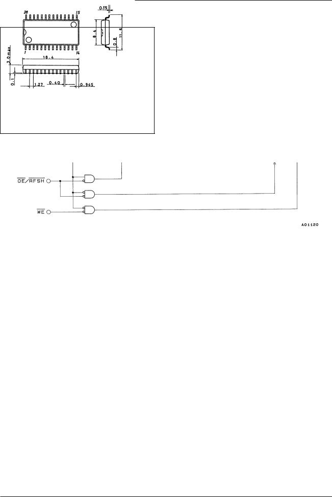
Package Dimensions
unit: mm
3012A-DIP28
[LC33832P, PL]
SANYO: DIP28
unit: mm
3133-DIP28
[LC33832S, SL]
SANYO: DIP28
• CE access time/OE access time/Cycle time/Current drain
|
|
|
|
Parameter |
|
LC33832P, S, M, PL, SL, ML |
|
||
|
|
|
|
|
|
|
|||
-70 |
-80 |
-10 |
|||||||
|
|
|
|
|
|
||||
|
|
|
|
|
|
|
|
||
|
|
|
70 ns |
80 ns |
100 ns |
||||
|
|
CE |
access time |
||||||
|
|
|
|
|
|
|
|
||
|
|
|
|
|
|
||||
|
OE access time |
30 ns |
35 ns |
40 ns |
|||||
|
|
|
|
|
|
|
|
||
|
Cycle time |
115 ns |
130 ns |
160 ns |
|||||
|
|
|
|
|
|
|
|
|
|
|
Current drain |
Operating |
65 mA |
60 mA |
50 mA |
||||
|
|
|
|
|
|||||
Standby |
|
1 mA/100 µA (L version) |
|
||||||
|
|
|
|
|
|
|
|||
|
|
|
|
|
|
|
|
|
|
SANYO Electric Co.,Ltd. Semiconductor Bussiness Headquarters
TOKYO OFFICE Tokyo Bldg., 1-10, 1 Chome, Ueno, Taito-ku, TOKYO, 110-8534 JAPAN
22897HA (OT)/52595TH (OT)/N1993JN/40893JN A8-9957, 58, 59, No. 4430-1/9
LC33832P, S, M, PL, SL, ML-70/80/10
unit : mm
3158-SOP28
[LC33832M, ML]
SANYO: SOP28
Block Diagram
No. 4430-2/9

LC33832P, S, M, PL, SL, ML-70/80/10
Pin Assignment |
Pin Functions |
|
||||||||
|
|
A0 to A14 |
Address input |
|||||||
|
|
|
|
|
|
|
|
|
|
|
|
|
|
|
|
|
|
|
Read/Write input |
||
|
|
|
|
|
WE |
|
|
|||
|
|
|
|
|
|
|
|
|
|
|
|
|
|
|
|
|
|
|
|
||
|
|
OE/RFSH |
Output-enable input/ refresh input |
|||||||
|
|
|
|
|
|
|
|
|
|
|
|
|
|
|
|
|
Chip-enable input |
||||
|
|
|
|
|
CE |
|
|
|||
|
|
|
|
|
|
|
|
|
|
|
|
|
I/O1 to I/O8 |
Data input/output |
|||||||
|
|
|
|
|
|
|
|
|
|
|
|
|
|
VCC |
Power supply |
||||||
|
|
|
GND |
Ground |
||||||
Functional Logic
|
|
|
|
|
|
|
|
|
|
|
|
|
|
|
|
|
|
CE |
|
OE |
|
|
WE |
|
A0 to A7 |
A8 to |
I/O1 |
|
|
|
State |
||||
|
|
|
|
/RFSH |
|
|
|
|
|
A14 |
to I/O8 |
|
|
|
|
||
|
|
|
|
|
|
|
|
|
|
|
|
|
|
|
|
|
|
|
H |
|
|
H |
|
|
X |
|
X |
X |
HZ |
|
Standby |
||||
|
L |
|
|
L |
|
|
H |
|
VX |
VX |
OUT |
|
Read |
||||
|
L |
|
|
H |
|
|
L |
|
VX |
VX |
IN |
|
Write |
||||
|
|
|
|
|
|
|
|
|
|
|
|
|
|
|
|
|
|
|
L |
|
|
H |
|
|
H |
|
VX |
X |
HZ |
|
CE-only refresh |
||||
|
H |
|
|
L |
|
|
X |
|
X |
X |
HZ |
|
Self-refresh |
||||
|
H |
|
NP |
|
|
X |
|
X |
X |
HZ |
|
Auto-refresh |
|||||
H ................... |
|
|
|
High-level input of VIN = 6.5 V to VIH (min) |
|
|
|
||||||||||
L .................... |
|
|
|
Low-level input of VIN = VIL (max) to –1.0 V |
|
|
|
||||||||||
X.................... |
|
|
|
Highor low-level input |
|
|
|
|
|
|
|||||||
NP................. |
|
|
|
Negative-polarity pulse input |
|
|
|
|
|
||||||||
VX |
|
|
|
“IN” when |
|
= L is confirmed, then “X” |
|
|
|
||||||||
|
|
|
CE |
|
|
|
|||||||||||
HZ................. |
|
|
|
High impedance |
|
|
|
|
|
|
|||||||
IN .................. |
|
|
|
Input state |
|
|
|
|
|
|
|
|
|||||
OUT.............. |
|
|
|
Output state |
|
|
|
|
|
|
|
|
|||||
No. 4430-3/9
 Loading...