


LC651154N

Ordering number : ENN*6728
91799RM (OT) No. 6278-1/39
Overview
The LC651154N/F/L and the LC651152N/F/L are the
small-scale control application versions of Sanyo’s
LC6500 series of 4-bit single-chip CMOS
microcontrollers, and feature the same basic architecture
and instruction set. These microcontrollers include an 8input 8-bit A/D converter and are appropriate for use in a
wide range of applications, from applications with a small
number of circuits and controls that were previously
implemented in standard logic to applications with a larger
scale such as home appliances, automotive equipment,
communications equipment, office equipment, and audio
equipment such as decks and players. Also note that since
these ICs provide the same basic functions (certain
functions and specifications do differ) as, and are pin
compatible with the earlier LC651104N/F/L and
LC651102N/F/L, they can replace those ICs in most cases.
Features
• Fabricated in a CMOS process for low power (A
standby function that can be invoked under program
control is also provided.)
• ROM/RAM
LC651154N/F/L — ROM: 4K × 8 bits,
RAM: 256 × 4 bits
LC651152N/F/L — ROM: 2K × 8 bits,
RAM: 256 × 4 bits
• Instruction set: The 80-instruction set common to the
LC6500 family
• Wide operating supply voltage range: 2.2 to 6.0 V
(L versions)
• Instruction cycle time: 0.92 µs (F versions)
• On-chip serial I/O function
• Flexible I/O ports
— Number of ports: 6 ports with a total of 22 pins
— All ports:
· Are I/O ports
· I/O voltage handling capacity: 15 V (maximum)
(Open-drain specification C, D, E, and F ports
only)
· Output current: 20 mA (maximum) sink current
(Are capable of directly driving an LED.)
— Support options to match application system
specifications
A. Open-drain output, internal pull-up resistor
specification: All ports, in bit units
B. Output level at reset specification: Ports C and D
can be specified to go to the high or low level in
4-bit units.
• Interrupt function
— Timer interrupts through an interrupt vector (Can be
tested under program control)
— INT pin and serial I/O full/empty interrupts through
an interrupt vector (Can be tested under program
control)
• Stack levels: 8 (Shared with the interrupt system.)
• Timers: 4-bit variable prescaler and 8-bit programmable
timers
• Clock oscillator options that match a wide range of
system specifications
— Oscillator circuit options:
Two-pin RC oscillator (N and L versions)
Two-pin ceramic oscillator (N, F, and L versions)
— Clock divider circuit options:
No divider, built-in divide-by-3, built-in divide-by-4
(N and L versions)
• Continuous square wave output (with a period 64 times
the cycle time)
• A/D converter (successive approximation)
— 8-bit precision with 8 input channels
• Watchdog timer
Preliminary
LC651154N, 651154F, 651154L, LC651152N, 651152F, 651152L
SANYO Electric Co.,Ltd. Semiconductor Company
TOKYO OFFICE Tokyo Bldg., 1-10, 1 Chome, Ueno, Taito-ku, TOKYO, 110-8534 JAPAN
Four-Bit CMOS Microcontrollers for
Small-Scale Control Applications
CMOS IC
Any and all SANYO products described or contained herein do not have specifications that can handle
applications that require extremely high levels of reliability, such as life-support systems, aircraft’s
control systems, or other applications whose failure can be reasonably expected to result in serious
physical and/or material damage. Consult with your SANYO representative nearest you before using
any SANYO products described or contained herein in such applications.
SANYO assumes no responsibility for equipment failures that result from using products at values that
exceed, even momentarily, rated values (such as maximum ratings, operating condition ranges, or other
parameters) listed in products specifications of any and all SANYO products described or contained
herein.

— RC circuit time constant
— Optional watchdog timer reset function from an
external pin
No. 6278-2/39
LC651154N, 651154F, 651154L, 651152N, 651152F, 651152L
Function Table
Parameter LC651154N/1152N LC651154F/1152F LC651154L/1152L
ROM
4096 × 8 bits (1154N) 4096 × 8 bits (1154F) 4096 × 8 bits (1154L)
Memory
2048 × 8 bits (1152N) 2048 × 8 bits (1152F) 2048 × 8 bits (1152L)
RAM 256 × 4 bits (1154/1152N) 256 × 4 bits (1154/1152F) 256 × 4 bits (1154/1152L)
Instructions
Instruction set 80 80 80
Table reference Supported Supported Supported
Interrupts 1 external, 1 internal 1 external, 1 internal 1 external, 1 internal
Timers
4-bit variable prescaler 4-bit variable prescaler 4-bit variable prescaler
On-chip functions
+ 8-bit timers + 8-bit timers + 8-bit timers
Stack levels 8 8 8
Standby function
Standby mode entered by the Standby mode entered by the Standby mode entered by the
HALT instruction supported HALT instruction supported HALT instruction supported
Number of ports 22 I/O port pins 22 I/O port pins 22 I/O port pins
Serial port
Input and output in 4 or 8 bit units Input and output in 4 or 8 bit units Input and output in 4 or 8 bit units
I/O voltage handling capability 15 V max. 15 V max. 15 V max.
I/O ports Output current 10 mA typ. 20 mA max. 10 mA typ. 20 mA max. 10 mA typ. 20 mA max.
I/O circuit types Open drain (n-channel) and pull-up resistor output options can be specified in 1-bit units
Output level at reset A high or low level output can be selected in port units (ports C and D only)
Square wave output Supported Supported Supported
Minimum cycle time 2.77 µs (V
DD
≥ 3 V) 0.92 µs (VDD≥ 2.5 V) 3.84 µs (VDD≥ 2.2 V)
Characteristics Supply voltage 3 to 6 V 2.5 to 6 V 2.2 to 6 V
Current drain 1.5 mA typ. 2 mA typ. 1.5 mA typ.
Oscillator element
RC (800/400 kHz typ.)
Ceramic 4 MHz
RC (400 kHz typ.)
Oscillator
Ceramic (400 k, 800 k, 1 MHz, 4 MHz) Ceramic (400 k, 800 k, 1 MHz, 4 MHz)
Divider circuit option 1/1, 1/3, 1/4 1/1 1/1, 1/3, 1/4
Other items Package DIP30S-D, MFP30S, SSOP30 DIP30S-D, MFP30S, SSOP30 DIP30S-D, MFP30S, SSOP30
Note: Recommendations for oscillator elements and oscillator circuit constants will be announced as the recommended circuits for these ICs are determined.
Verify the progress of these developments periodically.
Differences between the LC651154N/1152N and the LC651104N/1102N.
The table below lists the points that require care when converting an existing product that uses the LC651104N/1102N to
use the LC651154N/1152N.
No. 6278-3/39
LC651154N, 651154F, 651154L, 651152N, 651152F, 651152L
Parameter LC651154N/1152N LC651104N/1102N
Pdmax (1) : DIP 310 mW 250 mW
Allowable power dissipation Pdmax (2) : MFP 220 mW 150 mW
Pdmax (3) : SSOP 160 mW (No corresponding package)
f
CFOSC
Oscillator frequency precision: within ±2%
[OSC1, OSC2]
Changes in the recommended oscillator
Oscillator frequency precision: within ±4%
constants (See table 1.)
800 kHz typ. (V
DD
= 3 to 6 V) 900 kHz typ. (VDD= 4 to 6 V)
Constants changed: Rext = 5.6 kΩ ±1 % Constants changed: Rext = 4.7 kΩ ±1 %
Frequency variability (sample to sample): Frequency variability (sample to sample):
587 to 1298 kHz 634 to 1278 kHz
400 kHz typ. (V
DD
= 3 to 6 V) 400 kHz typ. (VDD= 3 to 6 V)
Frequency variability (sample to sample): Frequency variability (sample to sample):
290 to 616 kHz 276 to 742 kHz
Pull-up resistors Ru [RES] 200 to 800 kΩ(500 kΩ typ.) 300 to 700 kΩ (500 kΩ typ.)
Serial clock input clock cycle time t
CKCY
(1) [ SCK] min. 2.0 µs min. 3.0 µs
A/D converter characteristics Operating voltage V
DD
= 3 to 6 V VDD= 4 to 6 V
AV+ = V
DD
Reference input current
200 to 800 µA (500 µA typ.) 75 to 300 µA (150 µA typ.)
AV– = V
SS
IRIF [AV+, AV–]
Watchdog timer
Cw = 0.047 ±5% µF
V
DD
= 3 to 6 V VDD= 4 to 6 V
Rw = 680 ±1% kΩ
RI = 100 ±1% Ω
Package
DIP30S-D, MFP30S
DIP30S-D, MFP30S
An SSOP30 version was added.
Differences between the LC651154F/1152F and the LC651104F/1102F.
The table below lists the points that require care when converting an existing product that uses the LC651104F/1102F to
use the LC651154F/1152F.
Parameter LC651154F/1152F LC651104F/1102F
Pdmax (1) : DIP 310 mW 250 mW
Allowable power dissipation Pdmax (2) : MFP 220 mW 150 mW
Pdmax (3) : SSOP 160 mW (No corresponding package)
Operating supply voltage V
DD
2.5 to 6 V 4 to 6 V
Specifications for V
DD
= 4 to 6 V
Low-level input voltage V
IL
(n) The specifications for VDD= 2.5 to 6 V Specifications for VDD= 4 to 6 V
were added.
Oscillator characteristics
Ceramic oscillator Oscillator frequency precision: within ±2 % Oscillator frequency precision: within ±4 %
Oscillator frequency
Pull-up resistors Ru [RES] 200 to 800 kΩ(500 kΩ typ.) 300 to 700 kΩ (500 kΩ typ.)
Operating voltage
AD speed 1/1 : V
DD
= 3.5 to 6 V AD speed 1/1 : VDD= 4.5 to 6 V
AD speed 1/2 : V
DD
= 3 to 6 V AD speed 1/2 : VDD= 4 to 6 V
Reference input current
200 to 800 µA (500 µA typ.) 75 to 300 µA (150 µA typ.)
IRIF [AV+, AV–]
Package
DIP30S-D, MFP30S
DIP30S-D, MFP30S
An SSOP30 version was added.
Oscillator characteristics
Ceramic oscillator
Oscillator frequency
2-pin RC oscillator
Oscillator frequency
f
MOSC
[OSC1, OSC2]
f
CFOSC
[OSC1, OSC2]
A/D converter characteristics
AV+ = V
DD
AV– = V
SS
No. 6278-4/39
LC651154N, 651154F, 651154L, 651152N, 651152F, 651152L
Differences between the LC651154L/1152L and the LC651104L/1102L.
The table below lists the points that require care when converting an existing product that uses the LC651104L/1102L to
use the LC651154L/1152L.
Caution: Perform a full system evaluation and inspection after replacing the microcontroller.
Parameter LC651154L/1152L LC651104L/1102L
Pdmax (1) : DIP 310 mW 250 mW
Allowable power dissipation Pdmax (2) : MFP 220 mW 150 mW
Pdmax (3) : SSOP 160 mW (No corresponding package)
Operating supply voltage V
DD
2.2 to 6 V 2.5 to 6 V
Oscillator frequency precision: within ±2%
Changes in the recommended oscillator
Oscillator frequency precision: within ±4%
constants (See table 1.)
400 kHz typ. (V
DD
= 2.2 to 6 V) 400 kHz typ. (VDD= 2.5 to 6 V)
Frequency variability (sample to sample): Frequency variability (sample to sample):
290 to 841 kHz 276 to 742 kHz
Pull-up resistors Ru [RES] 200 to 800 kΩ(500 kΩ typ.) 300 to 700 kΩ (500 kΩ typ.)
Serial clock input clock cycle time t
CKCY
(1) [ SCK] min. 2.0 µs min. 6.0 µs
A/D converter characteristics Operating voltage V
DD
= 3 to 6 V VDD= 4 to 6 V
AV+ = V
DD
Reference input current
200 to 800 µA (500 µA typ.) 75 to 300 µA (150 µA typ.)
AV– = V
SS
IRIF [AV+, AV–]
Watchdog timer V
DD
= 2.2 to 6.0 V VDD= 2.5 to 6.0 V
Package
DIP30S-D, MFP30S
DIP30S-D, MFP30S
An SSOP30 version was added.
Oscillator characteristics
Ceramic oscillator
Oscillator frequency
2-pin RC oscillator
Oscillator frequency
f
CFOSC
[OSC1, OSC2]
f
MOSC
[OSC1, OSC2]
Pin Assignment
The pin assignment is the same for the DIP, MFP, and SSOP packages.
No. 6278-5/39
LC651154N, 651154F, 651154L, 651152N, 651152F, 651152L
System Block Diagram
No. 6278-6/39
LC651154N, 651154F, 651154L, 651152N, 651152F, 651152L
Pin Functions
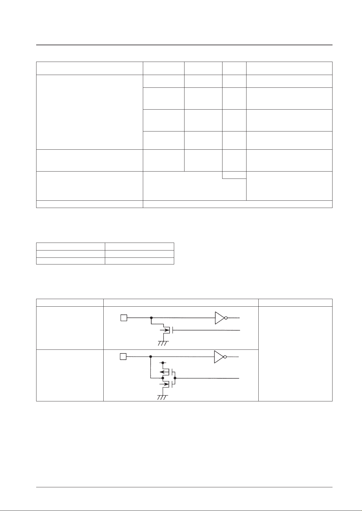
OSC1, OSC2: Connections for the oscillator capacitor and resistor or ceramic element TEST: IC testing.
RES: Reset INT: Interrupt request input
PA0 to PA3: Common I/O ports A0 to A3 SI: Serial input
PC0 to PC3: Common I/O ports C0 to C3 SO: Serial output
PD0 to PD3: Common I/O ports D0 to D3 SCK: Serial clock input output
PE0 to PE3: Common I/O ports E0 to E3 AD0 to AD7: A/D converter analog inputs
PF0 to PF3: Common I/O ports F0 to F3 AV
+
, AV–: A/D converter reference voltage inputs
PG0 to PG3: Common I/O ports G0 to G3 WDR: Watchdog timer reset input
Note: Pins SI, SO, SCK, and INT are shared function pins also used as PF0:3.
RAM: Data memory ROM: Program memory
F: Flag PC: Program counter
WR: Working register INT: Interrupt control
AC: Accumulator IR: Instruction register
ALU: Arithmetic and logic unit I.DEC: Instruction decoder
DP: Data pointer CF, CSF: Carry flag and carry save flag
E: E register ZF, ZSF: Zero flag and zero save flag
CTL: Control register EXTF: External interrupt request flag
OSC: Oscillator circuit TMF: Internal interrupt request flag
TM: Timer
STS: Status register
Shared with port F
Development Support
The following are provided for development with the LC651154 and LC651152.
• User’s manual
See the “LC651104/1102 User’s Manual.”
• Development tools manual
See the “Four-Bit Microcontroller EVA86000 Development Tools Manual.”
• Software manual
“LC65/66 Series Software Manual”
• Development tools
— Program development (EVA86000 System)
— On-chip EPROM microcontroller <LC65E1104> for program evaluation
No. 6278-7/39
LC651154N, 651154F, 651154L, 651152N, 651152F, 651152L
Pin Functions
Symbol
Number
I/O Function Option At reset
Handling when
of pins unused
V
DD
V
SS
1
—
—
Power supply — — —
OSC1 1 Input
• Connection for the RC circuit or ceramic oscillator
element used for the system clock oscillator
• Leave OSC2 open when an external clock input is
used.
(1) Two-pin RC oscillator or
external clock
(2) Two-pin ceramic oscillator
(3) Divider option
1. No divider
2. Divide-by-3
3. Divide-by-4
——
• I/O port A0 to A3
Input in 4-bit units (IP instruction)
Output in 4-bit units (OP instruction)
Testing in 1-bit units (BP and BNP instructions)
Set and reset in 1-bit units (SPB and RPB
instructions)
• PA3 is used for standby mode control
• Application must assure that chattering does not
occur on the PA3 input during HALT instruction
execution.
• All four pins have shared functions
PA0/AD0 - A/D converter input AD0
PA1/AD1 - A/D converter input AD1
PA2/AD2 - A/D converter input AD2
PA3/AD3 - A/D converter input AD3
(1) Open-drain output
(2) Pull-up resistor
Options (1) and (2) can be
specified in bit units
High-level
output (The
output nchannel
transistors in
the off state.)
Select the
open-drain
output option
and connect
to V
SS
.
OSC2 1
Output
PA0 to
PA3/
AD0 to
AD3
4 I/O
• I/O port C0 to C3
The port functions are identical to those of PA0 to
PA3. (See note.)
• The output during a reset can be selected to be
either high or low as an option.
Note: This port has no standby mode control
function.
(1) Open-drain output
(2) Pull-up resistor
(3) High-level output during reset
(4) Low-level output during reset
• Options (1) and (2) can be
specified in bit units
• Options (3) and (4) are
specified 4 bits at a time
• High-level
output
• Low-level
output
(Depending
on option
selected.)
The same as
for PA0 to
PA3
PC0 to
PC3
4 I/O
• I/O port D0 to D3
The port functions and options are identical to
those of PC0 to PC3.
The same as PC0 to PC3
The same as
PC0 to PC3
The same as
for PA0 to
PA3
PD0 to
PD3
4 I/O
Continued on next page.
No. 6278-8/39
LC651154N, 651154F, 651154L, 651152N, 651152F, 651152L
Continued from preceding page.
Symbol
Number
I/O Function Option At reset
Handling when
of pins unused
PE0-PE1/
WDR
2 I/O
• I/O port E0 to E1
Input in 4-bit units (IP instruction)
Output in 4-bit units (OP instruction)
Set and reset in 1-bit units (SPB and RPB
instructions)
Testing in 1-bit units (BP and BNP instructions)
• PE0 also has a continuous pulse (64·Tcyc) output
function.
• PE1 becomes the watchdog reset pin WDR when
selected for such as an option.
(1) Open-drain output
(2) Pull-up resistor
• Options (1) and (2) can be
specified in bit units
(3) Normal port PE1
(4) Watchdog reset WDR
• Either options (3) and (4)
may be specified.
High-level
output (The
output nchannel
transistors in
the off state.)
Identical to
those for PA0
to PA3
PF0/SI
PF1/SO
PF2/SCK
PF3/INT
4 I/O
• I/O port F0 to F3
The port functions and options are identical to
those of PE0 to PE1 (See note.)
• PF0 to PF3 have shared functions as the serial
interface pins and the INT input.
The function can be selected under program
control.
SI ... Serial input pin
SO ... Serial output pin
SCK ... Input and output of the serial clock signal
INT ... Interrupt request input
The serial I/O function can be switched between 4-
bit and 8-bit transfers under program control.
Note: There is no continuous pulse output function.
Identical to those for PA0 to PA3
Identical to
those for PA0
to PA3
The serial port
functions are
disabled.
The interrupt
source is set
to INT.
Identical to
those for PA0
to PA3
PG0-PG3/
AD4-AD7
4 I/O
• I/O port G0 to G3
The port functions and options are identical to
those of PE0 to PE1 (See note.)
Note: There is no continuous pulse output function.
• All four pins have shared functions.
PG0/AD4 - A/D converter input AD4
PG1/AD5 - A/D converter input AD5
PG2/AD6 - A/D converter input AD6
PG3/AD7 - A/D converter input AD7
Identical to those for PA0 to PA3
Identical to
those for PA0
to PA3
Identical to
those for PA0
to PA3
AV
+
1—
A/D converter reference voltage input — —
Connect to
V
SS
.
• System reset input
• Applications must provide an external capacitor for
the power-on reset.
• Apply a low level to this pin for 4 clock cycles to
effect and reset start.
———
AV
–
1—
RES 1 Input
• IC test pin
This pin must be connected to V
SS
during normal
operation.
——
This pin must
be connected
to V
SS
.
TEST 1 Input
No. 6278-9/39
LC651154N, 651154F, 651154L, 651152N, 651152F, 651152L
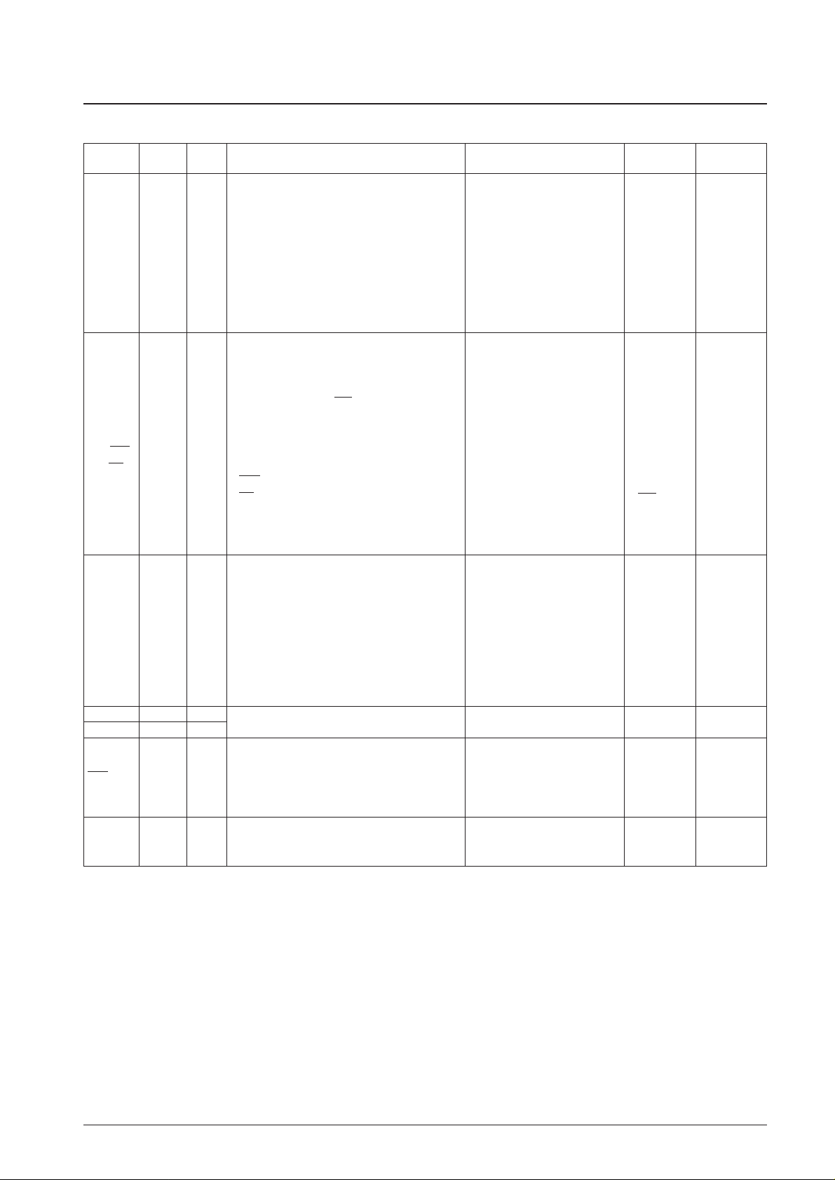
Oscillator Circuit Options
Option Circuit Conditions and other notes
Ceramic
oscillator element
Divider Circuit Options
Option Circuit Conditions and other notes
• This option can be used with any of the three oscillator
options.
• The oscillator frequency or external clock frequency must
not exceed 1444 kHz. (LC651154N, LC651152N)
• The oscillator frequency or external clock frequency must
not exceed 4330 kHz. (LC651154F, LC651152F)
• The oscillator frequency or external clock frequency must
not exceed 1040 kHz. (LC651154L, LC651152L)
• This option can only be used with the external clock and the
ceramic oscillator options.
• The oscillator frequency or external clock frequency must
not exceed 4330 kHz.
• This option can only be used with the external clock and the
ceramic oscillator options.
• The oscillator frequency or external clock frequency must
not exceed 4330 kHz.
Oscillator circuit
Caution: The following tables summarize the oscillator and divider circuit options. Use care when selecting these options.
Timing
generator
Oscillator circuit
Oscillator circuit
Timing
generator
Timing
generator
External clock
Two-pin RC oscillator
Ceramic oscillator
The OSC2 pin must be left open.
No divider
Built-in divide-by-three circuit
Built-in divide-by-four circuit
Divide-by-3
Divide-by-4
No. 6278-10/39
LC651154N, 651154F, 651154L, 651152N, 651152F, 651152L
LC651154N, LC651152N
Oscillator Options
Circuit type Frequency
Divider option
VDDrange Notes
(cycle time)
400 kHz 1/1 (10 µs) 3 to 6 V
Cannot be used with the divide-by-three
and divide-by-four options.
1/1 (5 µs) 3 to 6 V
800 kHz 1/3 (15 µs) 3 to 6 V
1/4 (20 µs) 3 to 6 V
1/1 (4 µs) 3 to 6 V
1 MHz 1/3 (12 µs) 3 to 6 V
1/4 (16 µs) 3 to 6 V
4 MHz
1/3 (3 µs) 3 to 6 V
Cannot be used with the no divider circuit
1/4 (4 µs) 3 to 6 V
option.
200 k to 1444 kHz 1/1 (20 to 2.77 µs) 3 to 6 V
600 k to 4330 kHz 1/3 (20 to 2.77 µs) 3 to 6 V
800 k to 4330 kHz 1/4 (20 to 3.70 µs) 3 to 6 V
Use the no divider circuit option and the 3 to 6 V
recommended circuit constants. If using other circuit
constants is unavoidable, the application must use a
frequency identical to the external clock and observe
the V
DD
range specification.
External clock used with the ceramic oscillator option External clock drive is not possible. To use external clock drive, select the 2-pin RC oscillator option.
LC651154F, LC651152F
Circuit type Frequency
Divider option
VDDrange Notes
(cycle time)
Ceramic oscillator 4 MHz 1/1 (1 µs) 2.5 to 6 V
External clock used with the 2-pin RC oscillator circuit 200 k to 4330 kHz 1/1 (20 to 0.92 µs) 2.5 to 6 V
External clock used with the ceramic oscillator option External clock drive is not possible. To use external clock drive, select the 2-pin RC oscillator option.
Ceramic oscillator
External clock used with the 2-pin RC oscillator circuit
Two-pin RC
No. 6278-11/39
LC651154N, 651154F, 651154L, 651152N, 651152F, 651152L
LC651154L, LC651152L
Circuit type Frequency
Divider option
VDDrange Notes
(cycle time)
400 kHz 1/1 (10 µs) 2.2 to 6 V
Cannot be used with the divide-by-three
and divide-by-four options.
1/1 (5 µs) 2.2 to 6 V
800 kHz 1/3 (15 µs) 2.2 to 6 V
1/4 (20 µs) 2.2 to 6 V
1/1 (4 µs) 2.2 to 6 V
1 MHz 1/3 (12 µs) 2.2 to 6 V
1/4 (16 µs) 2.2 to 6 V
Cannot be used with either the no divider
4 MHz 1/4 (4 µs) 2.2 to 6 V circuit option or the divide-by-three circuit
option.
200 k to 1040 kHz 1/1 (20 to 3.84 µs) 2.2 to 6 V
600 k to 3120 kHz 1/3 (20 to 3.84 µs) 2.2 to 6 V
800 k to 4160 kHz 1/4 (20 to 3.84 µs) 2.2 to 6 V
Use the no divider circuit option and the 2.2 to 6 V
recommended circuit constants. If using other circuit
constants is unavoidable, the application must use a
frequency identical to the external clock and observe
the V
DD
range specification.
External clock used with the ceramic oscillator option External clock drive is not possible. To use external clock drive, select the 2-pin RC oscillator option.
Port C and D Output Level During Reset Option
The output level during a reset can be selected from the two options below in 4-bit units for the C and D ports.
Port Output Type Option
The following two options may be selected for the I/O ports individually (bit units).
Watchdog Reset Option
This option allows the PE1/WDR pin to be selected either to be used as the normal port PE1 or to be used as the
watchdog reset pin WDR.
Option Conditions and other notes
High-level output during reset Ports C and D in 4-bit units
Low-level output during reset Ports C and D in 4-bit units
Option Circuit Applicable ports
Ceramic oscillator
External clock used with the 2-pin RC oscillator circuit
Two-pin RC
1. Open-drain output
2. Built-in pull-up resistor
Ports A, C, D, E, F, and G
LC651154N, 651152N
No. 6278-12/39
LC651154N, 651154F, 651154L, 651152N, 651152F, 651152L
Parameter Symbol Conditions Applicable pins and notes Ratings Unit
Maximum supply voltage V
DD
max V
DD
–0.3 to +7.0
Output voltage V
O
OSC2
Allowed up to the
generated voltage.
Input voltage
V
I
(1) OSC1 *
1
–0.3 to VDD+ 0.3
V
V
I
(2) TEST, RES, AV+, AV
–
–0.3 to VDD+ 0.3
V
IO
(1) PC0 to 3, PD0 to 3, PE0, 1, PF0 to 3 Open-drain specification ports –0.3 to +15
I/O voltage V
IO
(2) PC0 to 3, PD0 to 3, PE0, 1, PF0 to 3
Pull-up resistor specification ports
–0.3 to VDD+ 0.3
V
IO
(3) PC0 to 3, PG0 to 3 –0.3 to VDD+ 0.3
Peak output current I
OP
I/O ports –2 to +20
I
OA
Per single pin, averaged over 100 ms I/O ports –2 to +20
The total current for PC0 to PC3,
PC0 to 3
∑I
OA
(1)
PD0 to PD3, and PE0 to PE1 *
2
PD0 to 3 –15 to +100
mA
Average output current PE0 to 1
The total current for PF0 to PF3,
PF0 to 3
∑I
OA
(2)
PG0 to PG3, and PA0 to PA3 (See note 2.) *
2
PG0 to 3 –15 to +100
PA0 to 3
Pd max (1) Ta = –40 to +85°C (DIP package) 310
Allowable power dissipation Pd max (2) Ta = –40 to +85°C (MFP package) 220 mW
Pd max (3) Ta = –40 to +85°C (SSOP package) 160
Operating temperature Topr –40 to +85
°C
Storage temperature Tstg –55 to +125
Absolute Maximum Ratings at Ta = 25°C, VSS= 0 V
Parameter Symbol Conditions Applicable pins and notes
Ratings
Unit
min typ max
Operating supply voltage V
DD
V
DD
3.0 6.0
Standby supply voltage V
ST
RAM and register values retained*3V
DD
1.8 6.0
V
IH
(1) Output n-channel transistors off
Ports C, D, E, and F with
0.7 V
DD
13.5
open-drain specifications
VIH(2) Output n-channel transistors off
Ports C, D, E, and F with
0.7 V
DD
V
DD
pull-up resistor specifications
VIH(3) Output n-channel transistors off Port A, G 0.7 V
DD
V
DD
V
The INT, SCK, and SI
High-level input voltage VIH(4) Output n-channel transistors off pins with open-drain 0.8 V
DD
13.5
specifications
The INT, SCK, and SI
V
IH
(5) Output n-channel transistors off pins with pull-up resistor 0.8 V
DD
V
DD
specifications
V
IH
(6) VDD= 1.8 to 6.0 V RES 0.8 V
DD
V
DD
VIH(7) External clock specifications OSC1 0.8 V
DD
V
DD
Allowable Operating Ranges at Ta = –40 to +85°C, VSS= 0 V, VDD= 3.0 to 6.0 V (Unless otherwise specified.)
Continued on next page.
 Loading...