


Ordering number:ENN750F
Monolithic Linear IC
LA4440
6W 2-Channel, Bridge 19W typ Power Amplifier
Features
•Built-in 2 channels (dual) enabling use in stereo and bridge
amplifier applications. Dual : 6W×2 (typ.)
Bridge : 19W (typ.)
•Minimun number of external parts required.
•Small pop noise at the time of power supply ON/OFF and good starting balance.
•Good ripple rejection : 46dB (typ.)
•Good channel separation.
•Small residual noise (Rg=0).
•Low distortion over a wide range from low frequencies to high frequencies.
•Easy to design radiator fin.
•Built-in audio muting function.
•Built-in protectors.
a.Thermal protector
b.Overvoltage, surge voltage protector
c.Pin-to-pin short protector
Package Dimensions
unit:mm |
|
|
|
|
|
3023A-SIP14H |
|
|
|
||
|
|
|
[LA4440] |
|
|
|
|
|
37.0 |
|
4.5 |
|
|
|
|
|
|
|
|
|
30.0 |
|
|
15.0max |
13.8 |
|
|
R1.7 |
11.0 |
|
8.0 |
|
|
|
|
6.0 |
0.8min |
1 |
|
14 |
|
|
|
|
0.4 |
||
|
|
|
|
|
|
|
1.99 |
2.54 |
0.6 |
1.4 |
2.25 |
|
|
|
|
|
|
|
|
|
|
SANYO : SIP14H |
|
Specifications
Absolute Maximum Ratings at Ta = 25˚C
Parameter |
Symbol |
Conditions |
Ratings |
Unit |
|
|
|
|
|
|
|
Maximum supply voltage |
VCC max1 |
Quiescent (t=30s) |
25 |
V |
|
VCC max2 |
Operating |
18 |
V |
||
|
|||||
Surge supply voltage |
VCC(surge) |
t≤0.2s |
50 |
V |
|
Allowable power dissipation |
Pd max |
Tc=75˚C, See Pd max – Ta characteristic |
15 |
W |
|
Termal resistance |
θj-c |
Junction-to-case |
3 |
˚C/W |
|
|
|
|
|
|
|
Operating temperature |
Topr |
|
–20 to +75 |
˚C |
|
|
|
|
|
|
|
Storage temperature |
Tstg |
|
–40 to +150 |
˚C |
|
|
|
|
|
|
Recommended Operating Conditions at Ta = 25˚C
Parameter |
Symbol |
Conditions |
Ratings |
Unit |
|
|
|
|
|
|
|
Supply voltage |
VCC |
|
13.2 |
V |
|
Load resistance |
RL |
Stereo |
2 to 8 |
Ω |
|
|
|
|
|||
Bridge |
4 to 8 |
Ω |
|||
|
|
||||
|
|
|
|
|
 Any and all SANYO products described or contained herein do not have specifications that can handle applications that require extremely high levels of reliability, such as life-support systems, aircraft’s control systems, or other applications whose failure can be reasonably expected to result in serious physical and/or material damage. Consult with your SANYO representative nearest you before using any SANYO products described or contained herein in such applications.
 SANYO assumes no responsibility for equipment failures that result from using products at values that exceed, even momentarily, rated values (such as maximum ratings, operating condition ranges,or other parameters) listed in products specifications of any and all SANYO products described or contained herein.
SANYO Electric Co.,Ltd. Semiconductor Company
TOKYO OFFICE Tokyo Bldg., 1-10, 1 Chome, Ueno, Taito-ku, TOKYO, 110-8534 JAPAN
21500TH (KT)/90196RM/33194HO/8064KI/3233KI/O070KI, TS No.750–1/13

LA4440
Operating Characteristics at Ta = 25˚C, VCC=13.2V, RL=4Ω, f=1kHz, Rg=600Ω, with 100×100×1.5mm3 Al fin, See specified Test Circuit.
Parameter |
Symbol |
Conditions |
|
Ratings |
|
Unit |
|
|
|
||||
|
|
|
min |
typ |
max |
|
|
|
|
|
|
|
|
Quiescent current |
Icco |
|
|
100 |
200 |
mA |
|
|
|
|
|
|
|
Voltage gain |
VG |
|
49.5 |
51.5 |
53.5 |
dB |
|
|
|
|
|
|
|
Output power |
PO |
THD=10%, Stereo |
5.0 |
6.0 |
|
W |
|
|
|
|
|
||
THD=10%, Bridge |
|
19 |
|
W |
||
|
|
|
|
|||
|
|
|
|
|
|
|
Total harmonic distortion |
THD |
PO=1W |
|
0.1 |
1.0 |
% |
Input resistance |
ri |
|
|
30k |
|
Ω |
Output noise voltage |
VNO |
Rg=0 |
|
0.6 |
1.0 |
mV |
|
|
|
|
|
||
Rg=10kΩ |
|
1.0 |
2.0 |
mV |
||
|
|
|
||||
Ripple rejection ratio |
Rr |
VR=200mV, fR=100Hz, Rg=0 |
|
46 |
|
dB |
Channel separation |
Ch sep |
VO=0dBm, Rg=10kΩ |
45 |
55 |
|
dB |
Muting attenuation |
ATT |
VO=0dBm, VM=9V |
|
40 |
|
dB |
Gain difference between channels |
VG |
|
|
|
2 |
dB |
|
|
|
|
|
|
|
Equivalent Circuit Block Diagram
No.750–2/13
LA4440
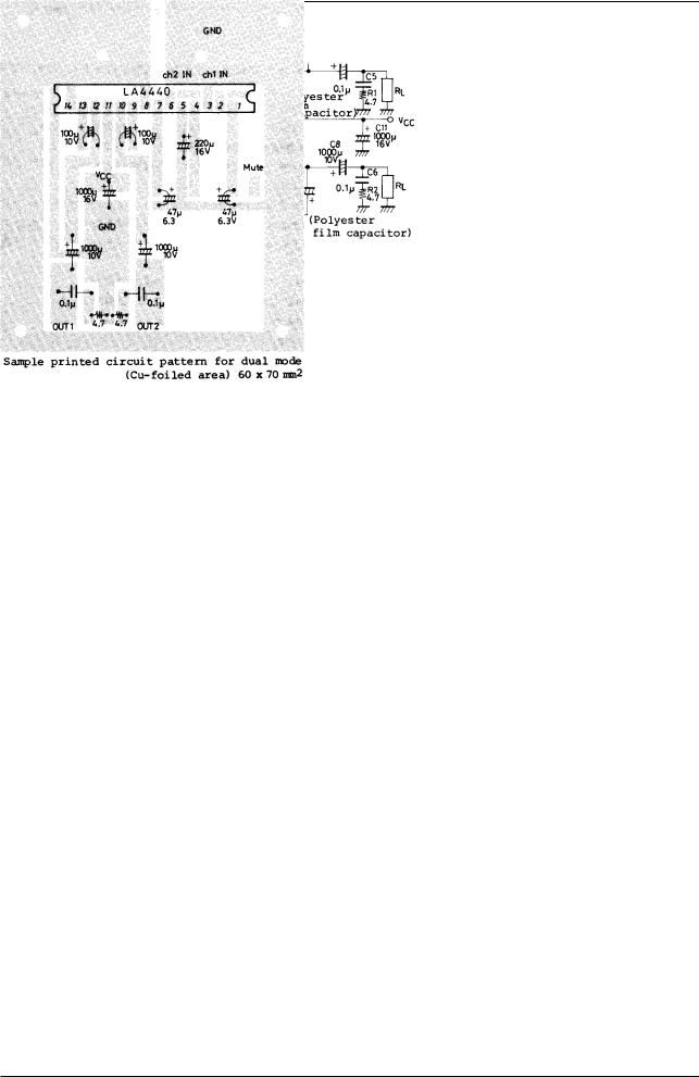
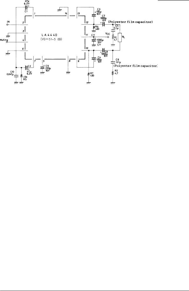
Sample Application Circuit 1. Stereo use
Sample Application Circuit 2. Bridge amplifier 1
No.750–3/13
LA4440
Sample Application Circuit 3. Bridge amplifier 2
Description of External Parts
C1 (C2) |
· Feedback capacitor : The low cutoff frequency depends on this capacitor. |
|
If the capacitance value is increased, the starting time is delayed. |
C3 (C4) |
· Bootstrap capacitor : If the capacitance value is decreased, the output at low frequencies goes lower. |
C5 (C6) |
· Oscillation preventing capacitor : Polyester film capacitor, being good in temperature characteristic, |
|
frequency characteristic, is used. |
|
The capacitance value can be reduced to 0.047 F depending on the stability of the board. |
C7 (C8) |
· Output capacitor : The low cutoff frequency depends on this capacitor. |
|
At the bridge amplifier mode, the output capacitor is generally connected. |
C9 |
· Decoupling capacitor :Used for the ripple filter. Since the rejection effect is saturated at a certain |
|
capacitance value, it is meaningless to increase the capacitance value more than required. This capaci- |
|
tor, being also used for the time constant of the muting circuit, affects the starting time. |
R1 (R2) |
· Filter resistor for preventing oscillation. |
R3 (R4) |
· Resistor for making input signal of inverting amplifier in Voltage Gain Adjust at Bridge Amplifier |
|
Mode (No. 1). |
R5 |
· Resistor for adjusting starting time in Voltage Gain Adjust at Bridge Amplifier Mode (No. 2) |
C10 |
· Capacitor for preventing oscillation in Voltage Gain Adjust at Bridge Amplifier Mode (No. 2) |
C11 |
· Power source capacitor. |
R6 (R7) |
· Used at bridge amplifier mode in order to increase discharge speed and to secure transient stability. |
Feaures of IC System and Functions of Remaining Pins
(a)Since the input circuit uses PNP transistors and the input potential is designed to be 0 bias, no input coupling capacitor is required and direct coupling is available. However, when slider contact noise caused by the variable resistor presents a problem, connect an capacitor in series with the input.
(b)The open-loop voltage gain is lowered and the negative feedback amount is reduced for stabilization. An increase in distortion resulted from the reduced negative feedback amount is avoided by use of the built-in unique distortion reduction circuit, and thus distortion is kept at 0.1% (typ.).
(c)A capacitor for oscillation compensation is contained as a means of reducing the number of external parts. The
capacitance value is 35pF which determines high cutoff frequency f |
(–3dB point) of the amplifier (f≈20kHz). |
H |
H |
(d)For preventing the IC from being damaged by a surge applied on the power line, an overvoltage protector is contained. Overvoltage setting is 25V. It is capable of withstanding up to 50V at giant pulse surge 200ms.
(e)No damege occurs even when power is applied at a state where pins 10, 11, and 12 are short-circuited with solder bridge, etc.
(f)To minimize the variations in voltage gain, feedback resistor RNF is contained and voltage gain (51.5dB) is fixed.
No.750–4/13
 Loading...