


LC662508A
Ordering number : EN5997
O1698RM (OT) No. 5997-1/17
Overview
The LC662516A, LC662512A, and LC662508A are 4-bit
CMOS microcontrollers that integrate on a single chip all
the functions required in a special-purpose telephone
controller, including ROM, RAM, I/O ports, a serial
interface, a DTMF generator, timers, and interrupt
functions. These microcontrollers are available in a 64-pin
package.
Features and Functions
• On-chip ROM capacities of 8, 12, and 16 kilobytes, and
an on-chip RAM capacity of 512 × 4 bits.
• Fully supports the LC66000 Series common instruction
set (128 instructions).
• I/O ports: 58 pins
• DTMF generator
This microcontroller incorporates a circuit that can
generate two sine wave outputs, DTMF output, or a
melody output for software applications.
• 8-bit serial interface: Two-wire interface (16-bit data
length. Supports cascade connection.)
• Instruction cycle time: 0.95 to 10 µs (at 3.0 to 5.5 V)
• Powerful timer functions and prescalers
— Time limit timer, event counter, pulse width
measurement, and square wave output using a 12-bit
timer.
— Time limit timer, event counter, PWM output, and
square wave output using an 8-bit timer.
— Time base function using a 12-bit prescaler.
• Powerful interrupt system with 11 interrupt factors and 8
interrupt vector locations.
— External interrupts: 3 factors/3 vector locations
— Internal interrupts: 8 factors/5 vector locations
(Waveform output internal interrupts: 3 factors and 1
vector; shared with external expansion interrupts)
• Flexible I/O functions
Selectable options include 20mA drive outputs, inverter
circuits, pull-up and open drain circuits.
• Optional runaway detection function (watchdog timer)
• 8-bit I/O functions
• Power saving functions using halt and hold modes.
• Packages: DIP64S, QIP64E (QFP64E)
• Evaluation ICs: LC665099 (evaluation chip) +
EVA86K-ECB662500
LC66E2516(on-chip EPROM microcontroller)
LC662508A, 662512A, 662516A
SANYO Electric Co.,Ltd. Semiconductor Bussiness Headquarters
TOKYO OFFICE Tokyo Bldg., 1-10, 1 Chome, Ueno, Taito-ku, TOKYO, 110-8534 JAPAN
Four-Bit Single-Chip Microcontrollers
with 8, 12, and 16 KB of On-Chip ROM
CMOS IC
Any and all SANYO products described or contained herein do not have specifications that can handle
applications that require extremely high levels of reliability, such as life-support systems, aircraft’s
control systems, or other applications whose failure can be reasonably expected to result in serious
physical and/or material damage. Consult with your SANYO representative nearest you before using
any SANYO products described or contained herein in such applications.
SANYO assumes no responsibility for equipment failures that result from using products at values that
exceed, even momentarily, rated values (such as maximum ratings, operating condition ranges, or other
parameters) listed in products specifications of any and all SANYO products described or contained
herein.
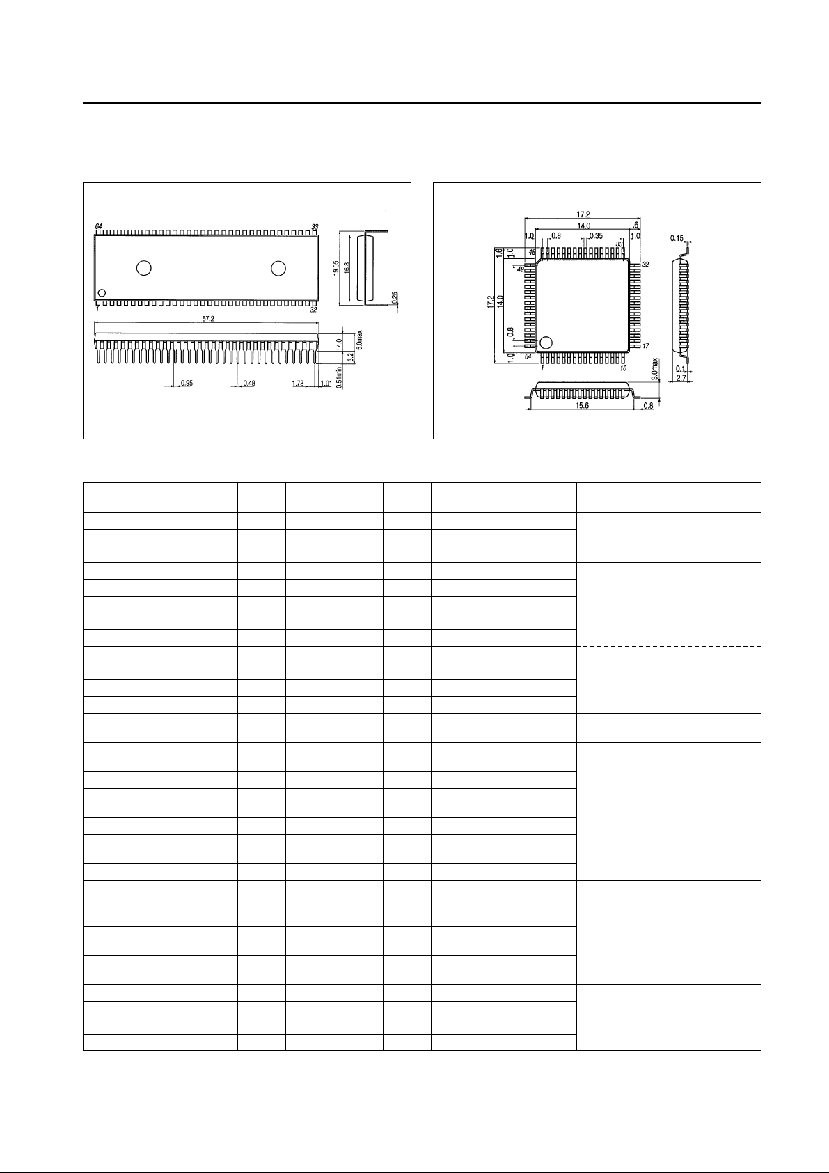
Package Dimensions
unit: mm
3071-DIP64S
unit: mm
3159-QFP64E
No. 5997-2/17
LC662508A, 662512A, 662516A
SANYO: DIP64S
[LC662508A,12A,16A]
SANYO: QFP64E
[LC662508A,12A,16A]
Series Organization
Type No.
No. of
ROM capacity
RAM
Package Features
pins capacity
LC66304A/306A/308A 42 4 K/6 K/8 KB 512 W DIP42S QFP48E
LC66404A/406A/408A 42 4 K/6 K/8 KB 512 W DIP42S QFP48E
LC66506B/508B/512B/516B 64 6 K/8 K/12 K/16 KB 512 W DIP64S QFP64A
LC66354A/356A/358A 42 4 K/6 K/8 KB 512 W DIP42S QFP48E
LC66354S/356S/358S 42 4 K/6 K/8 KB 512 W QFP44M
LC66556A/558A/562A/566A 64 6 K/8 K/12 K/16 KB 512 W DIP64S QFP64E
LC66354B/356B/358B 42 4 K/6 K/8 KB 512 W DIP42S QFP48E
Low-voltage high-speed versions
LC66556B/558B/562B/566B 64 6 K/8 K/12 K/16 KB 512 W DIP64S QFP64E
3.0 to 5.5 V/0.92 µs
LC66354C/356C/358C 42 4 K/6 K/8 KB 512 W DIP42S QFP48E 2.5 to 5.5 V/0.92 µs
LC662104A/06A/08A 30 4 K/6 K/8 KB 384 W DIP30SD MFP30S
LC662304A/06A/08A/12A/16A 42
4 K/6 K/8 K/12 K/16 KB
512 W DIP42S QFP48E
LC662508A/12A/16A 64 8 K/12 K/16 KB 512 W DIP64S QFP64E
LC665304A/06A/08A/12A/16A 48
4 K/6 K/8 K/12 K/16 KB
512 W DIP48S QFP48E
Dual oscillator support
3.0 to 5.5 V/0.95 µs
LC66E308 42 EPROM 8 KB 512 W
DIC42S QFC48
with window with window
LC66P308 42 OTPROM 8 KB 512 W DIP42S QFP48E
LC66E408 42 EPROM 8 KB 512 W
DIC42S QFC48
with window with window
LC66P408 42 OTPROM 8 KB 512 W DIP42S QFP48E
LC66E516 64 EPROM 16 KB 512 W
DIC64S QFC64
with window with window
LC66P516 64 OTPROM 16 KB 512 W DIP64S QFP64E
LC66E2108 30 EPROM 8 KB 384 W
LC66E2316 42 EPROM 16 KB 512 W
DIC42S QFC48
with window with window
LC66E2516 64 EPROM 16 KB 512 W
DIC64S QFC64
with window with window
LC66E5316 52/48 EPROM 16 KB 512 W
DIC52S QFC48
with window with window
LC66P2108 30 OTPROM 8 KB 384 W DIP30SD MFP30S
LC66P2316 42 OTPROM 16 KB 512 W DIP42S QFP48E
LC66P2516 64 OTPROM 16 KB 512 W DIP64S QFP64E
LC66P5316 48 OTPROM 16 KB 512 W DIP48S QFP48E
OTP
4.0 to 5.5 V/0.95 µs
Window evaluation versions
4.5 to 5.5 V/0.92 µs
Window and OTP evaluation versions
4.5 to 5.5 V/0.92 µs
On-chip DTMF generator versions
3.0 to 5.5 V/0.95 µs
Low-voltage versions
2.2 to 5.5 V/3.92 µs
Normal versions
4.0 to 6.0 V/0.92 µs
No. 5997-3/17
LC662508A, 662512A, 662516A
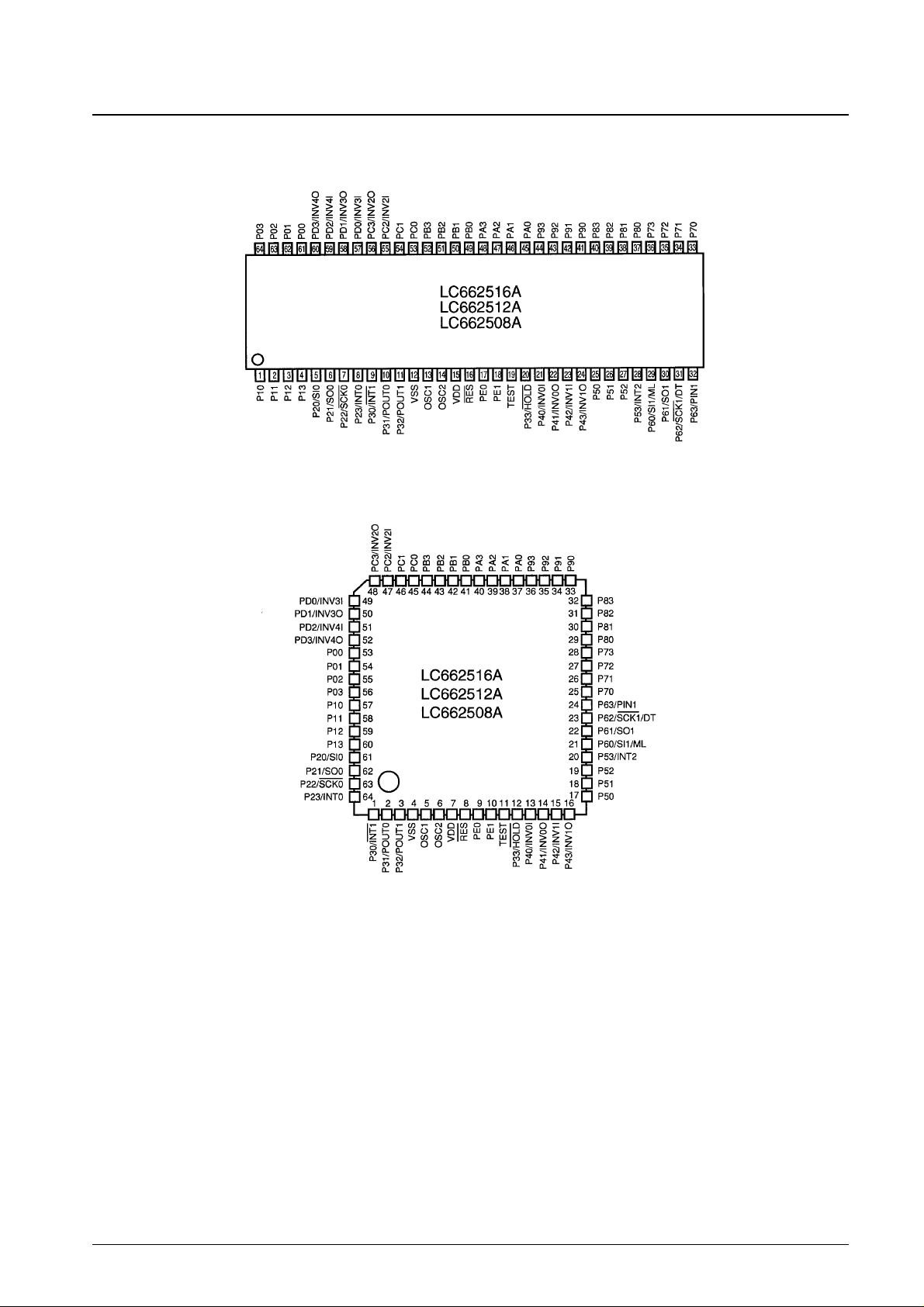
Pin Assignments DIP64S
We recommend the use of reflow-soldering techniques to solder-mount QFP packages.
Please consult with your Sanyo representative for details on process conditions if the package itself is to be directly
immersed in a dip-soldering bath (dip-soldering techniques).
Top view
QFP64E

System Block Diagram
No. 5997-4/17
LC662508A, 662512A, 662516A
Item
LC6650XB Series
LC6655XB Series LC6625XX Series
(Including the LC66599 evaluation chip)
System differences
65536 cycles 16384 cycles 16384 cycles
• Hardware wait time (number of
About 64 ms at 4 MHz (Tcyc = 1 µs) About 16 ms at 4 MHz (Tcyc = 1 µs) About 16 ms at 4 MHz (Tcyc = 1 µs)
cycles) when hold mode is cleared
• Value of timer 0 after a reset
(Including the value after hold mode Set to FF0. Set to FFC. Set to FFC.
is cleared)
• DTMF generator
None (Tools are handled with
None Yes
external devices.)
• Inverter array
None (Tools are handled with
None Yes
external devices.)
• Three-value inputs/comparator
Yes Yes None
inputs
• Three-state output from P31
None None Yes
and P32
• Using P0 to clear halt mode In 4-bit groups In 4-bit groups Can be specified for each bit.
For INT3, INT4, and INT5.
INT3, INT4, and INT5 can be used
• External extended interrupts (Tools are handled with external For INT3, INT4, and INT5.
with the internal functions.
devices.)
Shared with P90 (INT2)
• INT2 functions (Tools are handled with external Shared with P90 (INT2) Shared with P53 (INT2)
devices.)
Differences in main characteristics
• LC66506B/08B/12B/16B • 3.0 to 5.5 V/0.92 to 10 µs
• Operating power-supply voltage
4.0 to 6.0 V/0.92 to 10 µs • LC6655XA, 56XA
3.0 to 5.5 V/0.95 to 10 µs
and operating speed (cycle time)
• LC66E516/P516 2.2 to 5.5 V/3.92 to 10 µs
4.5 to 5.5 V/0.92 to 10 µs 3.0 to 5.5 V/1.96 to 10 µs
• Pull-up resistors P0, P1, P4, and P5: about 3 to 10 kΩ P0, P1, P4, and P5: about 3 to 10 kΩ P0, P1, P4, and P5: about 100 kΩ
• P2, P3, P6, P7, and PA: •P2, P3, P6, P7, and PA: P2, P3, P61, P63, and PA:
• Port voltage handling
15V handling 15V handling 15V voltage handling
• Others: Normal voltage • Others: Normal voltage Others: normal voltage
Differences between the LC665XX Series and the LC6625XX Series
• When DT, ML, and DP are used, only the SIO channel can be used for serial I/O.
• The INT3, INT4, and INT5 pins can be used with internal functions.
No. 5997-5/17
LC662508A, 662512A, 662516A
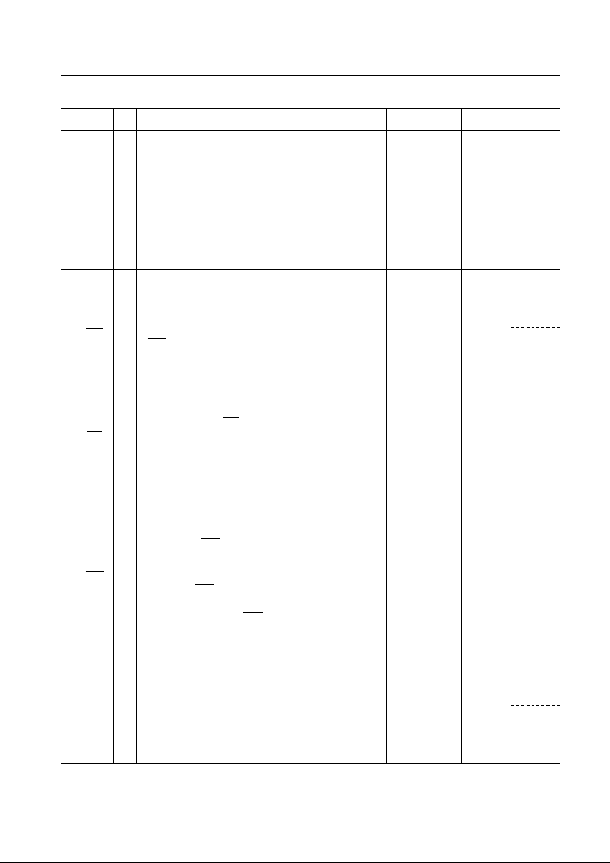
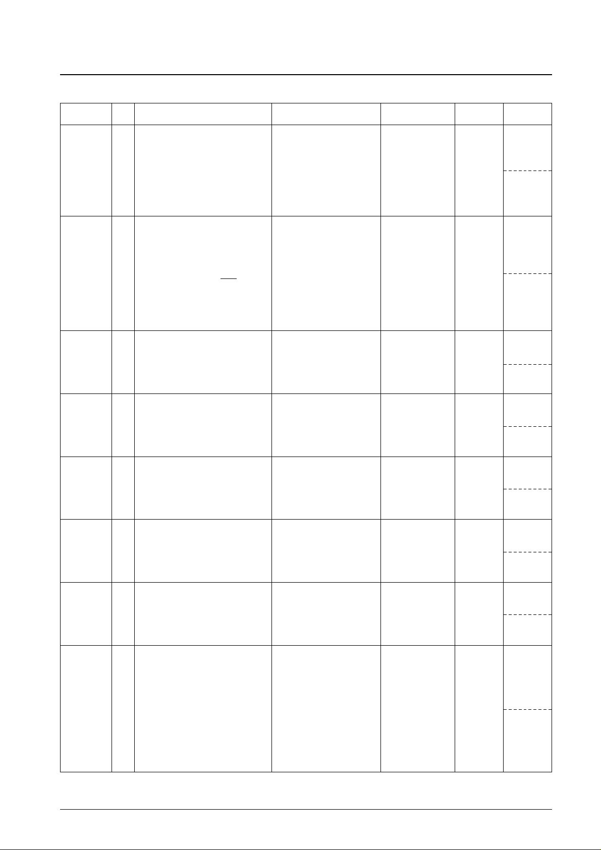
Pin Function Overview
Pin I/O Overview Output driver type Options
State after a Standby mode
reset operation
P00
P01
P02
P03
P10
P11
P12
P13
P20/SI0
P21/SO0
P22/SCK0
P23/INT0
P30/INT1
P31/POUT0
P32/POUT1
P33/HOLD
P40/INV0I
P41/INV0O
P42/INV1I
P43/INV1O
I/O ports P00 to P03
• Input or output in 4-bit or 1-bit units
• P00 to P03 support the halt mode
control function (This function can be
specified in bit units.)
I/O ports P10 to P13
Input or output in 4-bit or 1-bit units
I/O ports P20 to P23
• Input or output in 4-bit or 1-bit units
• P20 is also used as the serial input SI0
pin.
• P21 is also used as the serial output
SO0 pin.
• P22 is also used as the serial clock
SCK0 pin.
• P23 is also used as the INT0 interrupt
request pin, and also as the timer 0
event counting and pulse width
measurement input.
I/O ports P30 to P32
• Input or output in 3-bit or 1-bit units
• P30 is also used as the INT1 interrupt
request.
• P31 is also used for the square wave
output from timer 0.
• P32 is also used for the square wave
and PWM output from timer 1.
• P31 and P32 also support 3-state
outputs.
Hold mode control input
• Hold mode is set up by the HOLD
instruction when HOLD is low.
• In hold mode, the CPU is restarted by
setting HOLD to the high level.
• This pin can be used as input port P33
along with P30 to P32.
• When the P33/HOLD pin is at the low
level, the CPU will not be reset by a
low level on the RES pin. Therefore,
applications must not set P33/HOLD
low when power is first applied.
I/O ports P40 to P43
• Input or output in 4-bit or 1-bit units
• Input or output in 8-bit units when used
in conjunction with P50 to P53.
• Can be used for output of 8-bit ROM
data when used in conjunction with
P50 to P53.
• Dedicated inverter circuit (option)
I/O
I/O
I/O
I/O
I
I/O
• Pch: Pull-up MOS type
• Nch: Intermediate sink current
type
• Pch: Pull-up MOS type
• Nch: Intermediate sink current
type
• Pch: CMOS type
• Nch: Intermediate sink current
type
• Nch: +15V handling when OD
option selected
• Pch: CMOS type
• Nch: Intermediate sink current
type
• Nch: +15V handling when OD
option selected
• Pch: Pull-up MOS type
• CMOS type when the inverter
circuit option is selected
• Nch: Intermediate sink current
type
• Pull-up MOS or
Nch OD output
• Output level on
reset
• Pull-up MOS or
Nch OD output
• Output level on
reset
CMOS or Nch OD
output
CMOS or Nch OD
output
• Pull-up MOS or
Nch OD output
• Output level on
reset
• Inverter circuit
High or low
(option)
High or low
(option)
H
H
High or low
or inverter
I/O (option)
Hold mode:
Output off
Hold mode:
Output off
Hold mode:
Output off
Hold mode:
Output off
Hold mode:
Port output
off, inverter
output off
Halt mode:
Port output
retained,
inverter
output
continues
Halt mode:
Output
retained
Halt mode:
Output
retained
Halt mode:
Output
retained
Halt mode:
Output
retained
Continued on next page.
No. 5997-6/17
LC662508A, 662512A, 662516A
Continued from preceding page.
Pin I/O Overview Output driver type Options
State after a Standby mode
reset operation
P50
P51
P52
P53/INT2
P60/SI1/ML
P61/S01/
P62/
SCK1/DT/
P63/PIN1
P70
P71
P72
P73
I/O ports P50 to P53
• Input or output in 4-bit or 1-bit units
• Input or output in 8-bit units when used
in conjunction with P40 to P43.
• Can be used for output of 8-bit ROM
data when used in conjunction with
P40 to P43.
• P53 is also used as the INT2 interrupt
request.
I/O ports P60 to P63
• Input or output in 4-bit or 1-bit units
• P60 is also used as the SI1 serial input
pin and as the ML melody output pin.
• P61 is also used as the SO1 serial
output pin.
• P62 is also used as the SCK1 serial
clock pin and the DT dial tone output
pin.
• P63 is also used for the event count
input to timer 1.
Output ports P70 to P73
• Output in either 1-bit or 4-bit units.
• The contents of the output latch are
input by input instruction.
I/O
I/O
O
• Pch: Pull-up MOS type
• Nch: Intermediate sink current
type
• Pch: CMOS type
• Nch: Intermediate sink current
type
• Nch: +15V handling when OD
option selected (P61 and P63
only)
• Pch: Pu MOS
• Nch: Intermediate sink current
type
• Pull-up MOS or
Nch OD output
• Output level on
reset
CMOS or Nch OD
output
(When the ML or DT
output is used,
select open-drain
output and provide
an external pull-up
resistor.)
Pull-up MOS or Nch
OD output
High or low
(option)
H
H
Hold mode:
Output off
Hold mode:
Output off
Hold mode:
Output off
Halt mode:
Output
retained
Halt mode:
Output
retained
Halt mode:
Output
retained
P80
P81
P82
P83
Output ports P80 to P83
• Output in either 1-bit or 4-bit units.
• The contents of the output latch are
input by input instruction.
O
• Pch: Pu MOS
• Nch: Intermediate sink current
type
• CMOS or Pch OD
output
• Output level on
reset
High or low
(option)
P90
P91
P92
P93
I/O ports P90 to 93.
• Input or output in either 1-bit or 4-bit
units.
I/O
• Pch: CMOS
• Nch: Intermediate sink current
type
CMOS or Nch OD
output
H
PA0
PA1
PA2
PA3
Output ports PA0 to PA3
• Output in either 1-bit or 4-bit units.
• The contents of the output latch are
input by input instruction.
O
• Pch: Pu MOS
• Nch: +15-V handling when
OD option selected
Pull-up MOS or Nch
OD output
H
PB0
PB1
PB2
PB3
Output ports PB0 to PB3
• Output in either 1-bit or 4-bit units.
• The contents of the output latch are
input by input instruction.
O
• Pch: Pull-up MOS
• Nch: Intermediate sink current
type
Pull-up MOS or Nch
OD output
H
PC0
PC1
PC2/INV2I
PC3/INV2O
I/O ports PC0 to PC3
• Output in either 1-bit or 4-bit units.
• Dedicated input ports PC2 to PC3
• Dedicated inverter circuits (option)
I/O
• Pch: CMOS
• Nch: Intermediate sink current
type
• CMOS or Nch OD
output
• Inverter circuit
High or
inverter I/O
(option)
Hold mode:
Port output
off
Inverter
output off
Halt mode:
Port output
retained
Inverter
output
retained
Continued on next page.
Hold mode:
Output off
Halt mode:
Output
retained
Hold mode:
Output off
Halt mode:
Output
retained
Hold mode:
Output off
Halt mode:
Output
retained
Hold mode:
Output off
Halt mode:
Output
retained
 Loading...