


Ordering number : EN*5088C
CMOS IC
LC372100PP, PM, PT-10/20LV
2 MEG (262144 words × 8 bits) Mask ROM
Internal Clocked Silicon Gate
Preliminary
Overview
The LC372100PP, LC372100PM and LC372100PT are 262,144-word × 8-bit organization (2,097,152-bit) mask programmable read only memories.
The LC372100PP-10, LC372100PM-10 and LC372100PT-10 feature an access time of 100 ns, an OE access time of 40 ns, and a standby current of 30 µA, and are optimal for use in 5-V systems that require high-speed access.
The LC372100PP-20LV, LC372100PM-20LV and LC372100PT-20LV feature an access time of 200 ns, an OE access time of 80 ns, and a standby current of 4 µA, and thus are optimal for use in 3-V systems that use batteries. Additionally, they provide high-speed access in 3.3-V systems (3.0 to 3.6 V) with a 150-ns access time and a 60-ns OE access time.
These ROMs adopt the JEDEC standard pin assignment which allows them to replace EPROM easily. To prevent bus line collisions in multi-bus microcontroller systems, pin 24 can be mask programmed to be either active high or active low.
Features
•262144 words × 8 bits organization
•Power supply
LC372100PP, PM, PT-10: |
5.0 V ± 10% |
LC372100PP, PM, PT-20LV: |
2.7 to 3.6 V |
• Fast access time (tAA, tCA) |
|
LC372100PP, PM, PT-10: |
100 ns (max.) |
LC372100PP, PM, PT-20LV: |
200 ns (max.) |
|
150 ns |
• Operating current |
(VCC = 3.0 to 3.6 V) |
|
|
LC372100PP, PM, PT-10: |
70 mA (max.) |
LC372100PP, PM, PT-20LV: |
20 mA (max.) |
• Standby current |
|
LC372100PP, PM, PT-10: |
30 µA (max.) |
LC372100PP, PM, PT-20LV: |
5 µA (max.) |
•Full static operation (internal clocked type)
•Fully TTL compatible (5 V supply)
•3 state outputs
•JEDEC standard pin configuration
•Package type
LC372100PP-10/20LV: DIP32 (600 mil)
LC372100PM-10/20LV: SOP32 (525 mil) LC372100PT-10/20LV: TSOP32 (8 mm × 20 mm)
Package Dimensions
unit: mm
3192-DIP32
[LC372100PP]
SANYO: DIP32
unit: mm
3205-SOP32
[LC372100PM]
SANYO: SOP32
unit: mm
3224-TSOP32
[LC372100PT]
SANYO: TSOP32 (type-I)
SANYO Electric Co.,Ltd. Semiconductor Bussiness Headquarters
TOKYO OFFICE Tokyo Bldg., 1-10, 1 Chome, Ueno, Taito-ku, TOKYO, 110-8534 JAPAN
53098HA (OT)/51195TH (OT)/41095TH (OT) No. 5088-1/5
LC372100PP, PM, PT-10/20LV
Pin Assignments |
Pin Functions |
|
||
|
|
|
|
|
|
A0 to A17 |
Address input |
||
|
|
|
|
|
|
D0 to D7 |
Data output |
||
|
|
|
|
|
|
|
|
|
|
|
CE/CE |
Chip enable input |
||
|
|
|
|
|
|
|
|
|
|
|
OE/OE |
Output enable input |
||
|
|
|
|
|
|
VCC |
Power supply |
||
|
VSS |
Ground |
||
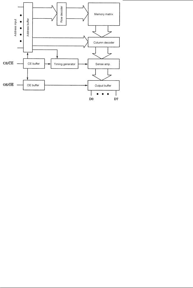
Block Diagram
Truth Table
|
|
|
|
|
|
|
|
CE/CE |
OE/OE |
Output |
Current drain |
||||
|
|
|
|
|
|
|
|
L/H |
X |
High-impedance |
Standby mode |
||||
|
|
|
|
|
|
|
|
H/L |
L/H |
High-impedance |
Operating mode |
||||
|
|
|
|
|
|
|
|
H/L |
H/L |
DOUT |
Operating mode |
||||
X: H or L level should be offered.
No. 5088-2/5
 Loading...