


Ordering number: EN3680C
Monolithic Linear IC
LA4485
5 W, Two-channel Power Amplifier with Very Few External Parts
Overview |
Package Dimensions |
The LA4485 is a 5 W, two-channel power amplifier IC that requires a minimum of external parts, making it ideal for radio cassette players and car stereo equipment.
The LA4485 eliminates the need for bootstrap capacitors, negative feedback capacitors, and oscillation prevention CR parts, all of which were necessities for power ICs previously. All of these functions are now on chip, keeping the number of external parts to an absolute minimum. The LA4485 is part of the Power (Stylish Power) Series, and supports two modes: dual and BTL.
Features
. 5 W × 2 output power in dual mode, and 15 W in BTL mode
. Minimum external parts for the Power Series count:
. 4 or 5 parts in dual mode; 3 or 4 parts in BTL mode Protection circuits
Overvoltage protection Thermal protection
. DC output short-circuit protection (to VCC and to GND)
. Circuitry designed to handle +VCC applied to the outputs
. Pop noise reduction
. Standby switch Muting function
Specifications
Maximum Ratings at Ta = 25°C
unit : mm
3107-SIP13H
SANYO : SIP13H
Parameter |
Symbol |
Conditions |
Ratings |
Unit |
|
|
|
|
|
Maximum supply voltage |
VCC max |
No signal |
24 |
V |
Surge supply voltage |
VCC surge * |
Based on the JASO standard |
50 |
V |
Peak output current |
IO peak |
Per channel |
3.3 |
A |
Allowable power dissipation |
Pd max |
With infinite heat sink |
15 |
W |
|
|
|
|
|
Operating temperature |
Topr |
|
±30 to +80 |
°C |
|
|
|
|
|
Storage temperature |
Tstg |
|
±40 to +150 |
°C |
|
|
|
|
|
*: By the π type B check point method.
Operating Conditions at Ta = 25°C
Parameter |
Symbol |
Conditions |
Ratings |
Unit |
|
|
|
|
|
|
|
Recommended supply voltage |
VCC |
|
13.2 |
V |
|
Supply voltage range |
VCC op |
Must not be over package Pd |
7.5 to 18 |
V |
|
Recommended load resistance range |
RL |
Dual |
2 to 8 |
Ω |
|
BTL |
4 to 8 |
Ω |
|||
|
|
SANYO Electric Co.,Ltd. Semiconductor Bussiness Headquarters
TOKYO OFFICE Tokyo Bldg., 1-10, 1 Chome, Ueno, Taito-ku, TOKYO, 110 JAPAN
73096HA(II)/D2893TS/9041TS No.3680-1/20
LA4485
Operating Characteristics at Ta = 25°C, V CC = 13.2 V, RL = 4 Ω, Rg = 600 Ω, f = 1 kHz, Dual
Parameter |
Symbol |
Conditions |
min |
typ |
max |
Unit |
|
|
|
|
|
|
|
Standby current |
Ist |
Pin 9 to GND, Standby switch OFF |
|
|
10 |
µA |
|
|
|
|
|
|
|
Quiescent supply current |
ICCO |
Rg = 0 |
40 |
80 |
160 |
mA |
Voltage gain |
VG1 |
Dual: VO = 0 dBm |
43 |
45 |
47 |
dB |
VG2 |
BTL: VO = 0 dBm |
|
51 |
|
dB |
|
|
|
|
||||
Output power |
PO1* |
Dual: THD = 10% |
4 |
5 |
|
W |
PO2 |
BTL: THD = 10% |
11 |
15 |
|
W |
|
|
|
|||||
Total harmonic distortion |
THD |
PO = 1 W |
|
0.15 |
0.8 |
% |
Channel separation |
CH sep |
VO = 0 dBm, Rg = 0 |
45 |
55 |
|
dB |
Output noise voltage |
VNO |
Rg = 0, 20 Hz to 20 kHz bandpass filter |
|
0.15 |
0.5 |
mV |
|
|
Rg = 0, 20 Hz to 20 kHz bandpass filter, |
|
|
|
|
Ripple rejection ratio |
SVRR |
fR = 100 Hz, VR = 0 dBm, decoupling capacitor |
40 |
50 |
|
dB |
|
|
connected |
|
|
|
|
*: PO1 = 6 W (typ) when VCC = 14.4 V Voff ± 250 mV for BTL-mode
Allowable power dissipation, Pd max ± W
Pd max ± Ta
Al heat sink mounting
Infinite heat sink conditions Mounting
torque
39 Nvcm. Flat washer with silicone grease applied
No heat sink
Ambient temperature, Ta ± °C
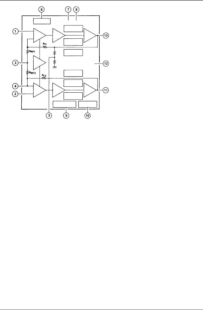
Equivalent Circuit Block Diagram
FILTER
Filter
CH1 IN
Input amp CH1
Small signal GND |
REF |
|
amp |
||
|
BTL IN
|
Input |
|
amp |
CH2 IN |
CH2 |
|
Large signal |
Small signal |
VCC |
VCC |
|
Output-to-ground |
|
|
short-circuit |
|
Pre |
protection |
|
Output |
||
drive |
||
amp |
amp |
|
|
Output-to-supply |
|
|
short-circuit |
|
|
protection |
|
|
Thermal shutdown |
|
|
protection |
Overvoltage protection
Output-to-supply short-circuit
Pre
protection
drive Output amp
amp
Output-to-ground short-circuit protection
Standby switch |
Mute |
CH1 OUT
Large signal GND
CH2 OUT
BTL OUT STANDBY |
MUTE |
No.3680-2/20
LA4485
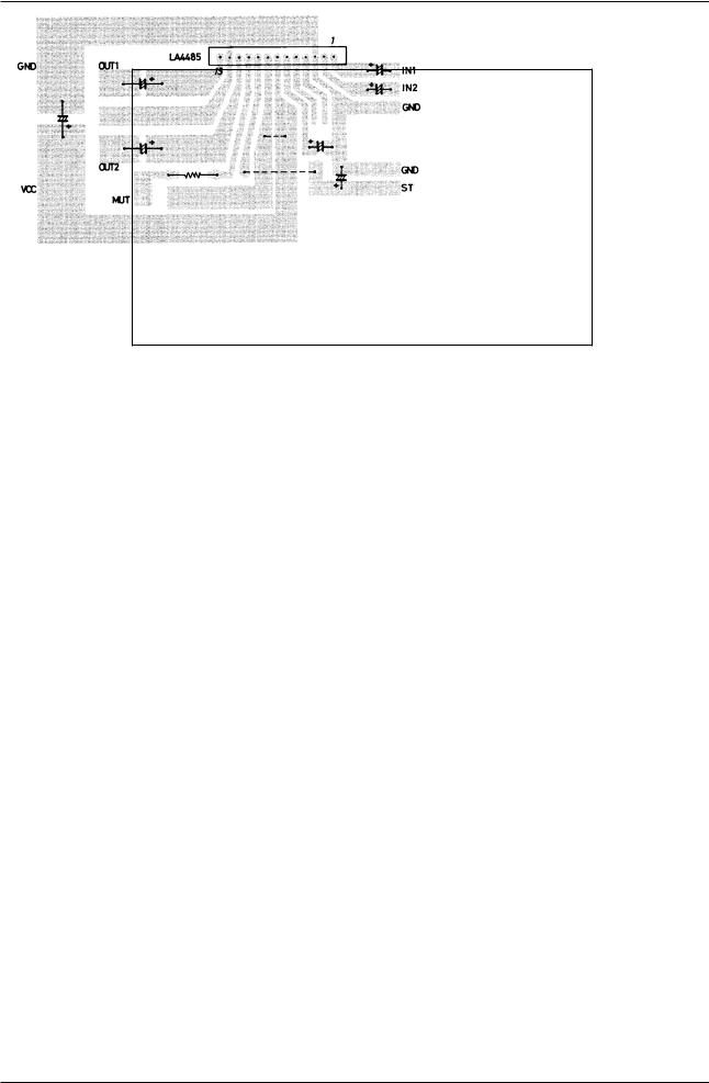
Recommended LA4485 External Parts Arrangement (Dual-mode)
95.0 × 67.0 mm2
IC Usage Notes
Maximum ratings
Care must be taken when operating the LA4485 close to the maximum ratings as small changes in the operating conditions can cause the maximum ratings to be exceeded, thereby breakdown will be caused.
Printed circuit board connections
Care must be taken when designing the circuit of printed board so as not to form feedback loops, particularly with the small-signal and large-signal ground connections.
Notes on LA4485 heatsink mounting
1.Mounting torque must be in the range 39 to 59 Nvcm.
2.The spacing of the tapped holes in the heatsink must match the spacing of the holes in the IC tab.
3.Use screws with heads equivalent to truss head machine screws and binding head machine screws stipulated by JIS for the mounting screws. Furthermore, washers must be used to protect the surface of the IC tab.
4.Make sure that there is no foreign matter, such as cutting debris, between the IC tab and the heatsink. If a heat conducting compound is applied between the contact surfaces, make sure that it is spread uniformly over the entire surface.
5.Because the heatsink mounting tab and the heatsink are at the same electric potential as the chip's GND (large signal GND), care must be taken when mounting the heatsink on more than one device.
6.The heatsink must be mounted before soldering the pins to the PCB.
Comparison of External Parts Required
External parts |
Existing device |
LA4485 |
|
|
|
Output coupling capacitors |
Yes |
Yes |
|
|
|
Input coupling capacitors |
Yes |
Yes |
|
|
|
Bootstrap capacitors |
Yes |
No |
|
|
|
Feedback capacitors |
Yes |
No |
|
|
|
Filter capacitor |
Yes |
Optional |
|
|
|
Phase compensating capacitor |
Yes |
No |
|
|
|
Oscillation-quenching mylar capacitors |
Yes |
No |
|
|
|
Oscillation-quenching resistors |
Yes |
No |
|
|
|
Others |
No |
Optional |
|
|
|
Total (for dual-mode) |
15 to 16 parts |
4 to 6 parts |
|
|
|
Note: Supply capacitors, contained within the power IC, are not counted in both existing and new devices.
No.3680-3/20
|
|
|
|
LA4485 |
|
|
|
|
|||
Operating Pin Voltages at VCC = 13.2 V |
|
|
|||
|
|
|
|
|
|
Pin No. |
Name |
Function |
Pin voltage (Reference value) |
|
|
|
|
|
|
|
|
1 |
CH1 IN |
Channel 1 input. |
1.4 |
V (2 VBE) |
|
2 |
CH2 IN |
Channel 2 input. |
1.4 |
V (2 VBE) |
|
3 |
SS GND |
Small-signal ground |
0 V |
|
|
|
|
|
|
|
|
4 |
BTL IN |
BTL-mode feedback input. |
45 mV |
|
|
|
|
|
|
|
|
5 |
BTL OUT |
BTL-mode feedback output. |
3.1 |
V (61/4 VCC) |
|
6 |
FILTER |
Filter capacitor connection. |
6.6 |
V (61/2 VCC) |
|
7 |
LS VCC |
Large-signal supply |
13.2 V (VCC) |
|
|
8 |
SS VCC |
Small-signal supply |
13.2 V (VCC) |
|
|
9 |
STANDBY |
Standby control input. |
5 V |
|
|
|
|
|
|
|
|
10 |
MUTE |
Mute control input. |
0 V |
|
|
|
|
|
|
|
|
11 |
CH2 OUT |
Channel 2 output. |
6.3 |
V |
|
|
|
|
|
|
|
12 |
LS GND |
Large-signal ground |
0 V |
|
|
|
|
|
|
|
|
13 |
CH1 OUT |
Channel 1 output. |
6.3 |
V |
|
|
|
|
|
|
|
Note: Each pin is so arranged lest the IC should be broken even if inserted reversely.
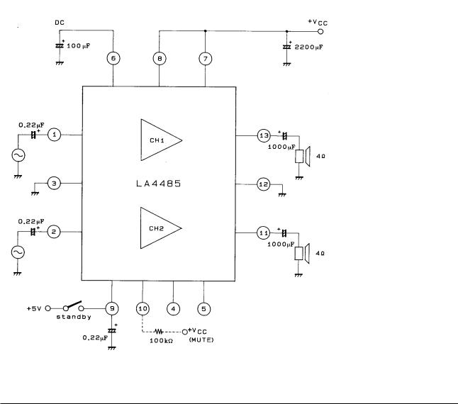
LA4485 Sample Application Circuit
No.3680-4/20
Output pin voltage, VN ± V
Standby current, Ist ± µA
Total harmonic distortion, THD ± %
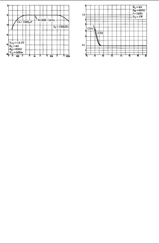
Response ± dB
VN ± VCC
RL = 4 Ω (dual)
Rg = 0 standby + 5 V
Overvoltage cutoff
VCC = 7.5 V
Cutoff for waveform carrying signal
Muting on
Supply voltage, VCC ± V lst ± VCC
CVCC = 0.15 µF (mylar) Rg = 0
Standby to GND
Supply voltage, VCC ± V
THD ± PO
Output power, P ± W f Response
LA4485
Quiescent supply current, ICCO ± mA
Output power, PO ± W
Total harmonic distortion, THD ± % Total harmonic distortion, THD ± %
ICCO ± VCC
RL = 4 Ω
Rg = 0
ICCO
Muting on
Supply voltage, VCC ± V
PO ± VIN
VCC = 13.2 V RL = 4 Ω
f = 1 kHz Rg = 600 Ω
Input voltage, VIN ± mV
THD ± f
Frequency, f ± Hz
THD ± VCC
Frequency, f ± Hz |
Supply voltage, VCC ± V |
No.3680-5/20

Output power, PO ± W
Power dissipation, Pd (2CH) ± W
Power dissipation, Pd (2CH) ± W
Power dissipation, Pd (2CH) ± W
LA4485
PO ± VCC |
|
|
|
|
|
|
(2CH) ± A |
|
|
|
CC |
|
|
|
Current drain, I |
Supply voltage, VCC ± V |
|
|
|
Pd ± PO |
|
|
|
Dual |
|
|
W |
RL = 2 Ω |
|
|
|
|
|
Power dissipation, Pd (2CH) ± |
|
|
|
|
|
Output power, P |
(1CH) ± W |
|
|
Pd ± PO |
|
|
|
|
Dual |
|
|
|
RL = 4 Ω |
Power dissipation, Pd (2CH) ± W |
|
|
|
|
|
Output power, P |
(1CH) ± W |
|
(2CH) |
Pd ± PO |
|
||
|
|
||
|
Dual |
Ω |
|
|
RL = 8 |
dissipation, Pd max ± W |
|
|
|
|
|
Output power, PO (1CH) ± W |
|
Allowable power |
|
|
|
||
ICC ± PO
Dual
Rg = 600 Ω f = 1 kHz
Output power, PO (1CH) ± W
Pd ± PO
Dual
RL = 3 Ω
Output power, P (1CH) ± W
Pd ± PO
Dual
RL = 6 Ω
Output power, P (1CH) ± W
Pd max ± VCC
Dual
Ta = 25°C
Supply voltage, VCC ± V
No.3680-6/20
 Loading...