


SANYO LC72342W, LC72342G, LC72341W, LC72341G, LC72343W Datasheet
...Ordering number : EN*5799
CMOS IC
LC72341G/W, LC72342G/W, LC72343G/W
Low-Voltage Single-Chip Microcontrollers with On-
Chip PLL and LCD Driver Circuits
Preliminary
Overview
The LC72341G/W, LC72342G/W, and LC72343G/W are single-chip microcontrollers with both a 1/4-duty 1/2-bias LCD driver circuit and a PLL circuit that can operate at up to 250 MHz integrated on the same chip. These ICs are ideal for use in portable audio equipment.
Reference frequencies of 1, 3, 5, 6.25, 12.5, and 25 kHz can be provided.
•Input frequency range
— FM band: 10 to 130 MHz
130 to 250 MHz
— AM band: 0.5 to 15 MHz
Functions
•High-speed programmable divider
•Program memory (ROM)
—LC72341G/W: 2048 words × 16 bits (4KB)
—LC72342G/W: 3072 words × 16 bits (6KB)
—LC72343G/W: 4096 words × 16 bits (8KB)
•Data memory (RAM)
—LC72341G/W: 128 words × 4 bits
—LC72342G/W: 192 words × 4 bits
—LC72343G/W: 256 words × 4 bits
•Instruction cycle time
—40 µs (for all single-word instructions.)
•Stack
—4 levels (LC72341G/W)
—8 levels (LC72342G/W, and LC72343G/W)
•LCD driver
—48 to 80 segments (1/4-duty 1/2-bias drive)
•Timer interrupts
—One timer circuit providing intervals of 1, 5, 10, and 50 ms.
•External interrupts
—One external interrupt (INT)
•A/D converter
—Two channels (5-bit successive approximation)
•Input ports
—7 (Of which two can be switched to function as A/D converter inputs)
•Output ports
—6 (Of which one can be switched to function as the BEEP tone output. Two ports are open-drain ports.)
• I/O |
ports |
—16 (Of which 8 can be selected to function as LCD ports as mask options.)
•PLL circuit
—Two types of dead band control are supported, and an unlock detection circuit is included.
Package Dimensions
unit: mm
3159-QFP64G
[LC72341G, 72342G, 72343G]
SANYO: QFP64G
unit: mm
3159-SQFP64
[LC72341W, 72342W, 72343W]
SANYO: SQFP64
SANYO Electric Co.,Ltd. Semiconductor Bussiness Headquarters
TOKYO OFFICE Tokyo Bldg., 1-10, 1 Chome, Ueno, Taito-ku, TOKYO, 110-8534 JAPAN
31398RM (OT) No. 5799-1/12
LC72341G/W, 72342G/W, 72343G/W
•IF counter
—HCTR input pin; 0.4 to 12 MHz
•Voltage detection circuit (VSENSE)
—Detects the VDD voltage and sets a flag
•External reset pin
—Restarts execution from location 0 when the CPU and PLL circuits are operating
•Power on reset circuit
—Starts execution from location 0 at power on.
•Universal counter
—20 bits
•Beep tones
—3.1 and 1.5 kHz
•Halt mode: The microcontroller operating clock is stopped
•Backup mode: The crystal oscillator is stopped
•An amplifier for a low-pass filter is built in
•CPU and PLL circuit operating voltage
—1.8 to 3.6 V
•RAM data retention voltage
—1.0 V or higher
•Packages
—QIP-64G : 0.8-mm lead pitch
—SQFP-64 : 0.5-mm lead pitch
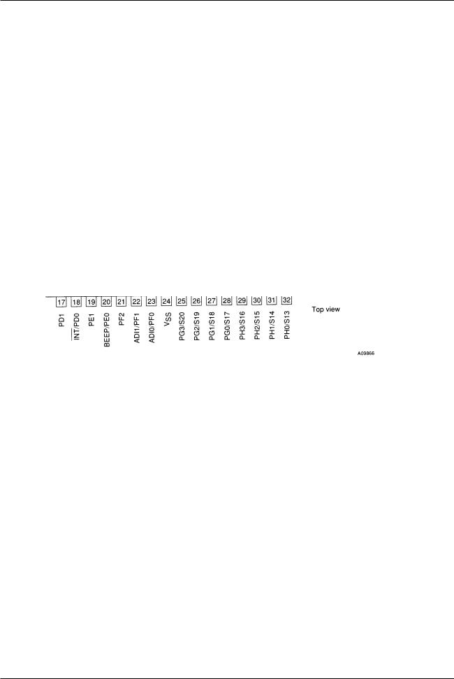
Pin Assignment
* PE0 and PE1 are open-drain outputs.
* The I/O ports can be set to input or output individually.
* The functions of the segment/general-purpose ports can be set in bit units.
No. 5799-2/12

LC72341G/W, 72342G/W, 72343G/W
Block Diagram
Divider
System clock generator
Pon reset
Bus
driver
Data latch/ Bus driver
Data latch/ Bus driver
Data latch/ Bus driver
Reference divider
Programmable divider
|
|
|
|
PLL data latch |
|
|
|
PLL control |
|
|
|
|
||||||||||||||||
|
|
|
|
|
|
|
|
|
|
|
|
|
|
|
|
|
|
|
|
|
|
|
|
|
|
|
|
|
|
Time base |
|
|
|
|
|
|
|
|
|
|
|
|
|
|
|
|
|
|
|
|
|
|
|
||||
|
|
count end |
|
|
|
|
|
|
|
|
|
|
|
|
|
|
|
|
|
|
|
|||||||
|
|
|
control |
|
|
|
|
|
|
|
|
|
|
|
|
|
|
|
|
|
|
|
|
|||||
|
|
|
|
|
|
|
|
|
|
|
|
|
|
|
|
|
|
|
|
|
|
|
|
|
|
|
||
|
|
|
|
|
|
|
|
|
|
|
|
|
|
|
|
|
|
|
|
|
||||||||
|
|
|
Universal counter |
|
|
|
|
|
|
|
|
|
|
|
|
|
|
|
|
|||||||||
|
|
|
|
(20 bits) |
|
|
|
|
|
|
|
|
|
|
|
|
|
|
|
|
|
|||||||
|
|
|
|
|
|
|
|
|
|
|
|
|
|
|
|
|
|
|
|
|
|
|
|
|
|
|
|
|
|
|
|
|
|
|
|
|
|
|
|
|
|
|
|
Address |
|
|
|||||||||||
|
|
|
|
|
|
|
|
|
|
|
|
|
|
|
decoder |
|
|
|||||||||||
|
|
|
|
|
|
|
|
|
|
|
|
|
|
|
|
|
|
|
|
|||||||||
|
|
|
|
|
|
|
|
|
|
|
|
|
|
|
|
|||||||||||||
|
|
|
|
|
|
|
|
|
|
|
|
|
|
|
Bank |
|
||||||||||||
|
|
|
|
|
|
|
|
|
|
|
|
|
|
|
|
|
|
|
|
|
|
|
||||||
|
|
|
|
|
|
|
|
|
|
|
|
|
|
|
|
|
|
|
|
|
|
|
|
|
|
|
|
|
|
|
|
|
|
|
|
|
|
|
|
|
|
|
|
|
|
|
|
|
|
Bus |
|
||||||
|
|
|
|
|
|
|
|
|
|
|
|
|
|
|
|
|
|
|
|
|
control |
|
||||||
|
|
|
|
|
|
|
|
|
|
|
|
|
|
|
|
|
|
|
|
|
|
|
|
|||||
|
|
|
|
|
|
|
|
|
|
|
|
|
|
|
|
|
|
|
|
|
|
|
|
|
|
|
|
|
|
|
|
|
|
|
|
|
|
|
|
|
|
|
|
|
|
|
|
|
|
Instruction |
|
||||||
|
|
|
|
|
|
|
|
|
|
|
|
|
|
|
|
|
|
|
|
|
decoder |
|
||||||
|
|
|
|
|
|
|
|
|
|
|
|
|
|
|
|
|
|
|
|
|
|
|
|
|
||||
|
|
|
|
|
|
|
|
|
|
|
|
|
|
|
|
|
|
|
|
|
|
|
|
|
|
|
|
|
|
|
|
|
Address decoder |
|
|
|
|
|
|
|
|
|
|
|
|
|
Skip |
||||||||||
|
|
|
|
|
|
|
|
|
|
|
|
|
|
|
|
|
|
|
|
|
|
|
|
|
||||
|
|
|
|
|
|
|
|
|
|
|
|
|
|
|
|
|
|
|
|
|
|
|
|
|
|
|
|
|
|
|
|
|
|
|
|
|
|
|
|
|
|
|
|
|
|
JMP CAL |
|
|
|
|
|||||||
|
|
|
|
|
|
|
|
|
|
|
|
|
|
|
|
|
Return |
|
|
|
|
|||||||
|
|
|
|
Program counter |
|
|
|
|
||||||||||||||||||||
|
|
|
|
|
|
|
|
|
interrupt |
|
|
|
|
|
|
|||||||||||||
|
|
|
|
|
|
|
|
|
|
|
|
|
|
|
|
|
|
|
|
|
||||||||
|
|
|
|
|
|
|
|
|
|
|
|
|
|
|
|
|||||||||||||
|
|
|
|
|
|
|
|
|
|
|
|
|
|
|
|
|
reset |
|
|
|
|
|||||||
|
|
|
|
|
|
|
|
|
|
|
|
|
|
|
|
|
|
|
|
|
|
|||||||
|
|
|
|
|
|
|
|
|
|
|
|
|
|
|
|
|
|
|
|
|
|
|
|
|
|
|
|
|
|
|
|
|
|
|
Stack |
|
|
|
|
|
|
Bank |
|
|
|
||||||||||||
|
|
|
|
|
|
|
|
|
|
|
|
|
|
|
|
|
|
|
|
|
|
|
||||||
|
|
|
|
|
|
|
|
|
|
|
|
|
|
|
|
|
|
|
|
|
|
|
|
|
||||
|
|
|
|
|
|
|
|
|
|
|
|
|
|
|
|
|
|
|
|
|
|
|||||||
Latch |
|
|
|
|
|
|
|
|
|
|
|
|
|
|
|
|
Judge |
|
||||||||||
|
A |
|
|
|
|
|
|
|
|
|
|
|
|
|
|
|
|
|
|
|
|
|
|
|
|
|||
|
|
|
|
|
|
|
|
|
|
|
|
|
|
|
|
|
|
|
|
|
|
|
|
|||||
Latch
B
Phasedetector
LCD
Port
Lach
driver
Data latch/ Bus driver
Data latch/ Bus driver
Doubler
circuit
Common
driver
Beep tone
Data latch/ Bus driver
Timer 0
Data latch/ Bus driver
Data bus
No. 5799-3/12

LC72341G/W, 72342G/W, 72343G/W
Specifications
Absolute Maximum Ratings at Ta = 25°C, VSS = 0 V
Parameter |
Symbol |
Conditions |
Ratings |
Unit |
|
|
|
|
|
|
|
Maximum supply voltage |
VDD max |
|
–0.3 to +4.0 |
V |
|
Input voltage |
VIN |
All input pins |
–0.3 to VDD + 0.3 |
V |
|
Output voltage |
VOUT1 |
AOUT, PE |
–0.3 to +15 |
V |
|
VOUT2 |
All output pins except VOUT1 |
–0.3 to VDD to + 0.3 |
V |
||
|
|||||
|
IOUT1 |
PC, PD, PG, PH, EO |
0 to 3 |
mA |
|
|
IOUT2 |
PB |
0 to 1 |
mA |
|
Output current |
IOUT3 |
AOUT, PE |
0 to 2 |
mA |
|
|
IOUT4 |
S1 to S20 |
300 |
µA |
|
|
IOUT5 |
COM1 to COM4 |
3 |
mA |
|
Allowable power dissipation |
Pd max |
Ta = –20 to +70°C |
300 |
mW |
|
|
|
|
|
|
|
Operating temperature |
Topr |
|
–20 to +70 |
°C |
|
|
|
|
|
|
|
Storage temperature |
Tstg |
|
–45 to +125 |
°C |
|
|
|
|
|
|
Allowable Operating Ranges at Ta = –20 to 70°C, VDD = 1.8 to 3.6 V
Parameter |
Symbol |
|
|
Conditions |
|
Ratings |
|
Unit |
|
|
|
|
|
|
|||||
min |
typ |
max |
|||||||
|
|
|
|
|
|
||||
|
|
|
|
|
|
|
|
|
|
Supply voltage |
VDD1 |
|
CPU and PLL operating voltage |
1.8 |
3.0 |
3.6 |
V |
||
VDD2 |
|
Memory retention voltage |
1.0 |
|
|
V |
|||
|
|
|
|
||||||
|
VIH1 |
|
VIH2, VIH3, AMIN, FMIN, |
0.7 VDD |
|
VDD |
V |
||
|
|
Input ports except HCTR and XIN. |
|
||||||
Input high-level voltage |
|
|
|
|
|
|
|
|
|
VIH2 |
|
|
|
|
|
|
|
||
|
RES |
0.8 VDD |
|
VDD |
V |
||||
|
|
|
|||||||
|
VIH3 |
|
Port PF |
0.6 VDD |
|
VDD |
V |
||
|
VIL1 |
|
VIL2, VIL3, AMIN, FMIN, |
0 |
|
0.3 VDD |
V |
||
|
|
Input ports except HCTR and XIN. |
|
||||||
Input low-level voltage |
|
|
|
|
|
|
|
|
|
VIL2 |
|
|
|
|
|
|
|
||
|
RES |
0 |
|
0.2 VDD |
V |
||||
|
|
|
|||||||
|
VIL3 |
|
Port PF |
0 |
|
0.2 VDD |
V |
||
|
VIN1 |
|
XIN |
0.5 |
|
0.6 |
Vrms |
||
Input amplitude |
VIN2 |
|
FMIN, AMIN |
0.035 |
|
0.35 |
Vrms |
||
VIN3 |
|
FMIN |
0.05 |
|
0.35 |
Vrms |
|||
|
|
|
|||||||
|
VIN4 |
|
HCTR |
0.035 |
|
0.35 |
Vrms |
||
Input voltage range |
VIN5 |
|
ADI0, ADI1 |
0 |
|
VDD |
V |
||
|
FIN1 |
|
XIN : CI ≤ 35 kΩ |
70 |
75 |
80 |
kHz |
||
|
FIN2 |
|
FMIN : VIN2, VDD1 |
10 |
|
130 |
MHz |
||
Input frequency |
FIN3 |
|
FMIN : VIN3, VDD1 |
130 |
|
250 |
MHz |
||
FIN4 |
|
AMIN (H) : VIN2, VDD1 |
2 |
|
40 |
MHz |
|||
|
|
|
|||||||
|
FIN5 |
|
AMIN (L) : VIN2, VDD1 |
0.5 |
|
10 |
MHz |
||
|
FIN6 |
|
HCTR : VIN4, VDD1 |
0.4 |
|
12 |
MHz |
||
Electrical Characteristics at Ta = –20 to 70°C, VDD = 1.8 to 3.6 V (in the allowable operating ranges)
Parameter |
Symbol |
|
|
Conditions |
|
Ratings |
|
Unit |
|||
|
|
|
|
|
|||||||
min |
typ |
max |
|||||||||
|
|
|
|
|
|
|
|
||||
|
|
|
|
|
|
|
|
|
|
|
|
|
IIH1 |
XIN : VI = VDD = 3.0 V |
|
|
3 |
µA |
|||||
Input high-level current |
IIH2 |
FMIN, AMIN, HCTR : VI = VDD = 3.0 V |
3 |
8 |
20 |
µA |
|||||
IIH3 |
Ports PA/PF (with no pull-down resistor), PC, |
|
|
3 |
µA |
||||||
|
|
|
|||||||||
|
|
|
|
|
|
|
|
||||
|
PD, PG, and PH. RES: VI = VDD = 3.0 V |
|
|
||||||||
|
|
|
|
|
|
||||||
|
IIL1 |
XIN : VI = VDD = VSS |
|
|
–3 |
µA |
|||||
Input low-level current |
IIL2 |
FMIN, AMIN, HCTR : VI = VDD = VSS |
–3 |
–8 |
–20 |
µA |
|||||
IIL3 |
Ports PA/PF (with no pull-down resistor), PC, |
|
|
–3 |
µA |
||||||
|
|
|
|||||||||
|
|
|
|
|
|
|
|
||||
|
PD, PG, and PH. RES: VI = VDD = VSS |
|
|
||||||||
|
|
|
|
|
|
||||||
Input floating voltage |
VIF |
PA/PF with pull-down resistors used |
|
|
0.05 VDD |
V |
|||||
Pull-down resistance |
RPD1 |
PA/PF with pull-down resistors used, VDD = 3 V |
75 |
100 |
200 |
kΩ |
|||||
Hysteresis |
VH |
|
0.1 VDD |
0.2 VDD |
|
V |
|||||
|
RES |
|
|
||||||||
Voltage doubler reference voltage |
DBR4 |
Ta = 25°C, referenced to VDD, C3 = 0.47 µF |
1.3 |
1.5 |
1.7 |
V |
|||||
Voltage doubler step-up voltage |
DBR1, 2, 3 |
Ta = 25°C, C1 = 0.45 µF, C2 = 0.47 µF, no load |
2.7 |
3.0 |
3.3 |
V |
|||||
|
|
|
|
|
|
|
|
|
|
|
|
No. 5799-4/12
 Loading...