


LC7265
Received Frequency Display for Radio Receivers
Features
.
Displays received frequency of each band of FM, MW, LW
(LED static display).
.
Counts local oscillation frequency and displays received
frequency.
.
Number of display digits : FM-5 digits, MW-4 digits, LW-3
digits.
.
Covers intermediate frequencies shown below.
FM : +10.700, +10.725, +10.750, +10.675 MHz
–10.700, –10.725, –10.675, –10.650 MHz
MW, LW : +450 kHz : 10 kHz step display
+450 kHz : 1 kHz step display
+455 kHz : 1 kHz step display
+469 kHz : 1 kHz step display
.
Contains blanking circuit to turn off display.
.
Contains hold circuit to hold display contents.
.
Uses crystal resonator having 7.2 MHz reference frequency.
.
Uses LB3500 (÷8 prescaler) jointly at the time of FM
reception.
.
Supply voltage V
DD
:4.5Vto10V
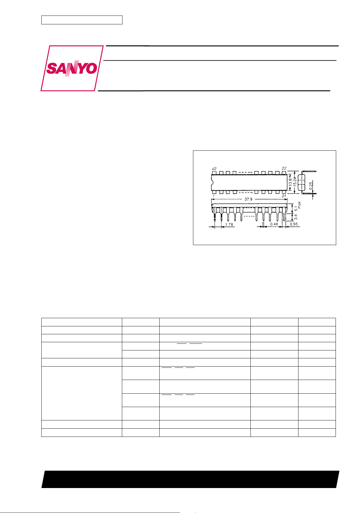
Package Dimensions
unit : mm
3025B-DIP42S
[LC7265]
SANYO : DIP42S
Specifications
Absolute Maximum Ratings atTa=25
°
C, V
SS
=0V
Parameter Symbol Conditions Ratings Unit
Maximum supply voltage V
DD
max –0.3 to +11 V
Input voltage V
IN
All input pins –0.3 to V
DD
+0.3 V
Output voltage V
O
1X
OUT
, HLD, 50 Hz, output: off –0.3 to V
DD
+0.3 V
V
O
2 Output pins other than V
O
1 0 to 15 V
Allowable power dissipation Pd max Ta % 65
°
C 550 mW
Allowable power dissipation of
segment outputs
Pd (seg)1 MHz, b&c, b&e, V
DD
= 4.5 to 6.5 V,
I
OL
=33mA
30 mW
Pd (seg) 2 Other outputs, V
DD
= 4.5 to 6.5 V,
I
OL
= 16.5 mA
15 mW
Pd (seg) 3 MHz, b&c, b&e, V
DD
= 6.0 to 10 V,
I
OL
=36mA
25 mW
Pd (seg) 4 Other outputs, V
DD
= 6.0 to 10 V,
I
OL
=18mA
12 mW
Operating temperature Topr –30 to +65
°
C
Storage temperature Tstg –40 to +125
°
C
Ordering number: EN 1197F
CMOS IC
LC7265
SANYO Electric Co.,Ltd. Semiconductor Bussiness Headquarters
TOKYO OFFICE Tokyo Bldg., 1-10, 1 Chome, Ueno, Taito-ku, TOKYO, 110-8534 JAPAN
63098HA(II)/6088YT/9105KI/3173KI/D162KI/7162KI/6242KI,TS No.1197-1/6
Allowable Operating Ranges atTa=25
°
C, V
DD
= 4.5 to 10 V, V
SS
=0V
Parameter Symbol Conditions min typ max Unit
Supply voltage V
DD
4.5 10 V
Input high-level voltage
V
IH
1 A/F, BLK 0.7V
DD
V
DD
V
V
IH
2 FIF1, FIF2, FIF3, AIF1, AIF2 0.9V
DD
V
DD
V
Input low-level voltage
V
IL
1 A/F, BLK 0 0.3V
DD
V
V
IL
2 FIF1, FIF2, FIF3, AIF1, AIF2 0 0.1V
DD
V
Input frequency
f
IN
1
FMI, sine wave, capacitive coupling,
V
IN
1 = 0.7Vp-p
1 18 MHz
f
IN
2
AMI, sine wave, capacitive coupling,
V
IN
2 = 0.5Vp-p*
0.5 3 MHz
f
IN
3X
IN
0.2 7.5 MHz
Input amplitude
V
IN
1
FMI, sine wave, capacitive coupling,
f
IN
1=1to18MHz
0.7 0.9V
DD
Vp-p
V
IN
2
AMI, sine wave, capacitive coupling,
f
IN
2 = 0.5 to 3 MHz
0.5* 0.9V
DD
Vp-p
V
IN
3
X
IN
, sine wave, capacitive coupling,
f
IN
3 = 0.2 to 7.5 MHz
1.0 0.9V
DD
Vp-p
Segment current
Iseg1 MHz, b&e, b&c
030mA
Iseg2 Other outputs 0 15 mA
*: For f
IN
2 = 0.5 MHz to 0.9 MHz and V
DD
=8to10V,V
IN
2 min = 1.0 Vp-p applies.
Electrical Characteristics atTa=25
°
C, V
DD
= 4.5 to 10 V, V
SS
=0V
Parameter Symbol Conditions min typ max Unit
Input high-level current
I
IH
1 FIF1, FIF2, FIF3, AIF1, AIF2 V
I
=V
DD
010µA
I
IH
2 BLK V
I
=V
DD
02µA
Input low-level current
I
IL
1 FIF1, FIF2, FIF3, AIF1, AIF2 V
I
=V
SS
010µA
I
IL
2 BLK V
I
=V
SS
02µA
I
IL
3 A/F V
I
=V
SS
20 500 µA
Input floating voltage V
IF
A/F V
I
= open 0.8V
DD
V
DD
V
Input/output high-level leakage
current
I
OFF
HLD, output off, V
I
=V
DD
02µA
Output low-level voltage
V
OL
1 HLD, output on, I
O
=1mA 01V
V
OL
2
b&e, b&c, MHz V
DD
= 4.5 to 10 V,
I
OL
=30mA
0 0.7 V
V
OL
3
Segments other than above
V
DD
= 4.5 to 10 V, I
OL
=15mA
0 0.7 V
V
OL
4 50 Hz, I
O
= 0.2 mA 0 1.0 V
Input high-level threshold voltage Vth HLD
0.4V
DD
0.5V
DD
0.7V
DD
V
Output off leakage current I
OFF
2 All segments output pins, V
O
= 13 V, output off 0 10 µA
Current drain I
DD
FM mode, A/F = open or V
DD
,f
IN
1 = 18 MHz,
0.7Vp-p or (AM mode, A/F = V
SS
,f
IN
2=
3 MHz, 0.5Vp-p) f
IN
3 = 7.2 MHz, 1Vp-p
FIF1, FIF2, FIF3 = V
DD
AIF1, AIF2 = V
DD
HLD, BLK = V
DD
other pins open
018mA
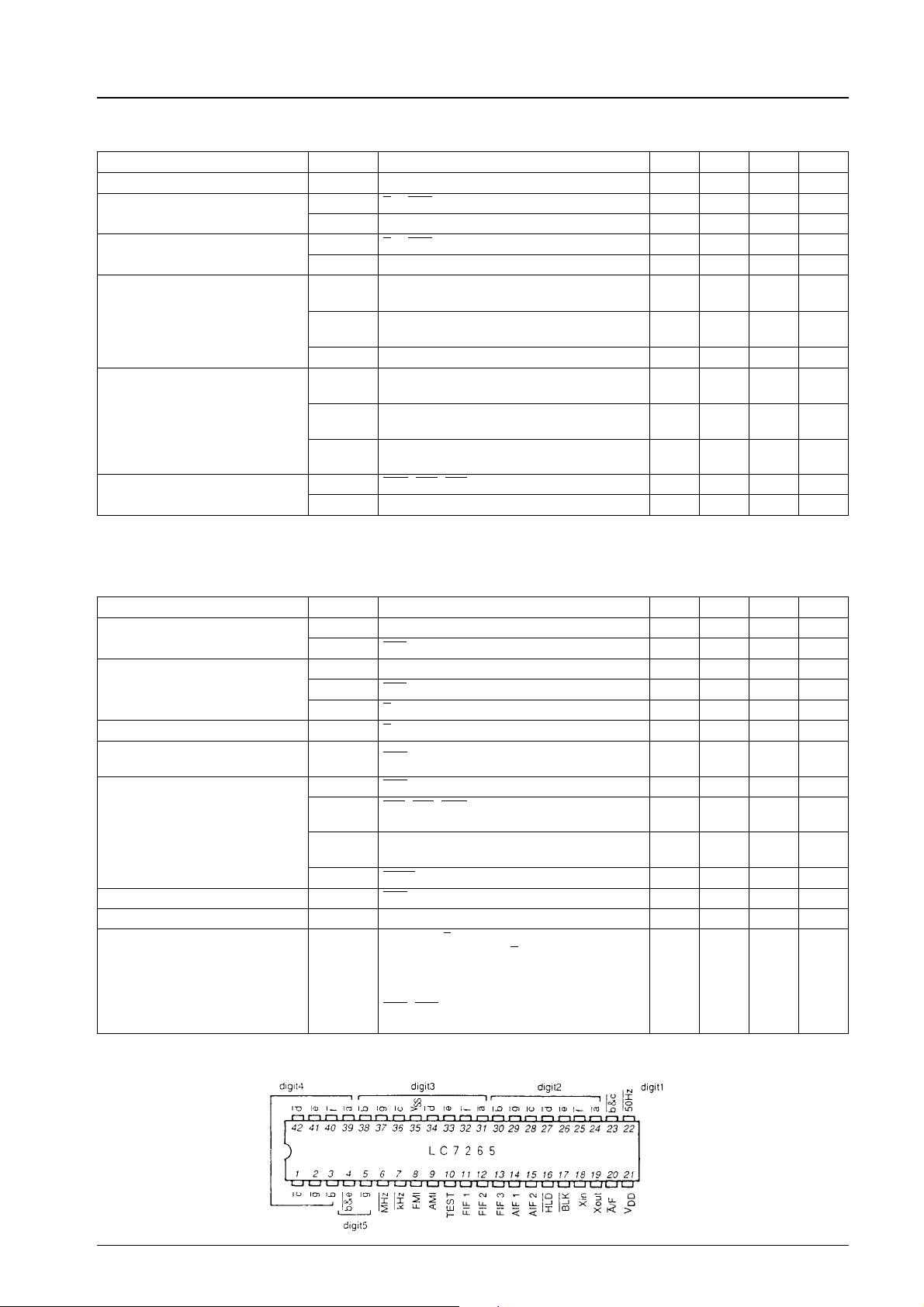
Pin Assignment
Top view
LC7265
No.1197-2/6
 Loading...