


LC75834E
Overview
The LC75834E, LC75834W, and LC75834JE are 1/4-duty
general-purpose LCD drivers that can be used for
frequency display in electronic tuners under the control of
a microcontroller. The LC75834E and LC75834W can
drive an LCD with up to 136 segments directly, the
LC75834JE can drive an LCD with up to 120 segments
directly. The LC75834E and LC75834W and LC75834JE
can also control up to 8 general-purpose output ports.
Since the LC75834E, LC75834W, and LC75834JE use
separate power supply systems for the LCD drive block
and the logic block, the LCD driver block power-supply
voltage can be set to any voltage in the range 2.7 to 6.0
volts, regardless of the logic block power-supply voltage.
Features
• Supports both 1/4 duty 1/2 bias and 1/4 duty 1/3 bias
LCD drive under serial data control.
LC75834E, LC75834W: up to 136 segments
LC75834JE: up to 120 segments
(without the S9, S18, S27, S34 segment output pins
from the LC75834E, LC75834W)
• Serial data input supports CCB* format communication
with the system controller.
• Serial data control of the power-saving mode based
backup function and all the segments forced off function
• Serial data control of switching between the segment
output port and the general-purpose output port
functions
• High generality, since display data is displayed directly
without decoder intervention.
• Independent V
LCD
for the LCD driver block (V
LCD
can
be set to any voltage in the range 2.7 to 6.0 volts,
regardless of the logic block power-supply voltage.)
• The INH pin can force the display to the off state.
• RC oscillator circuit
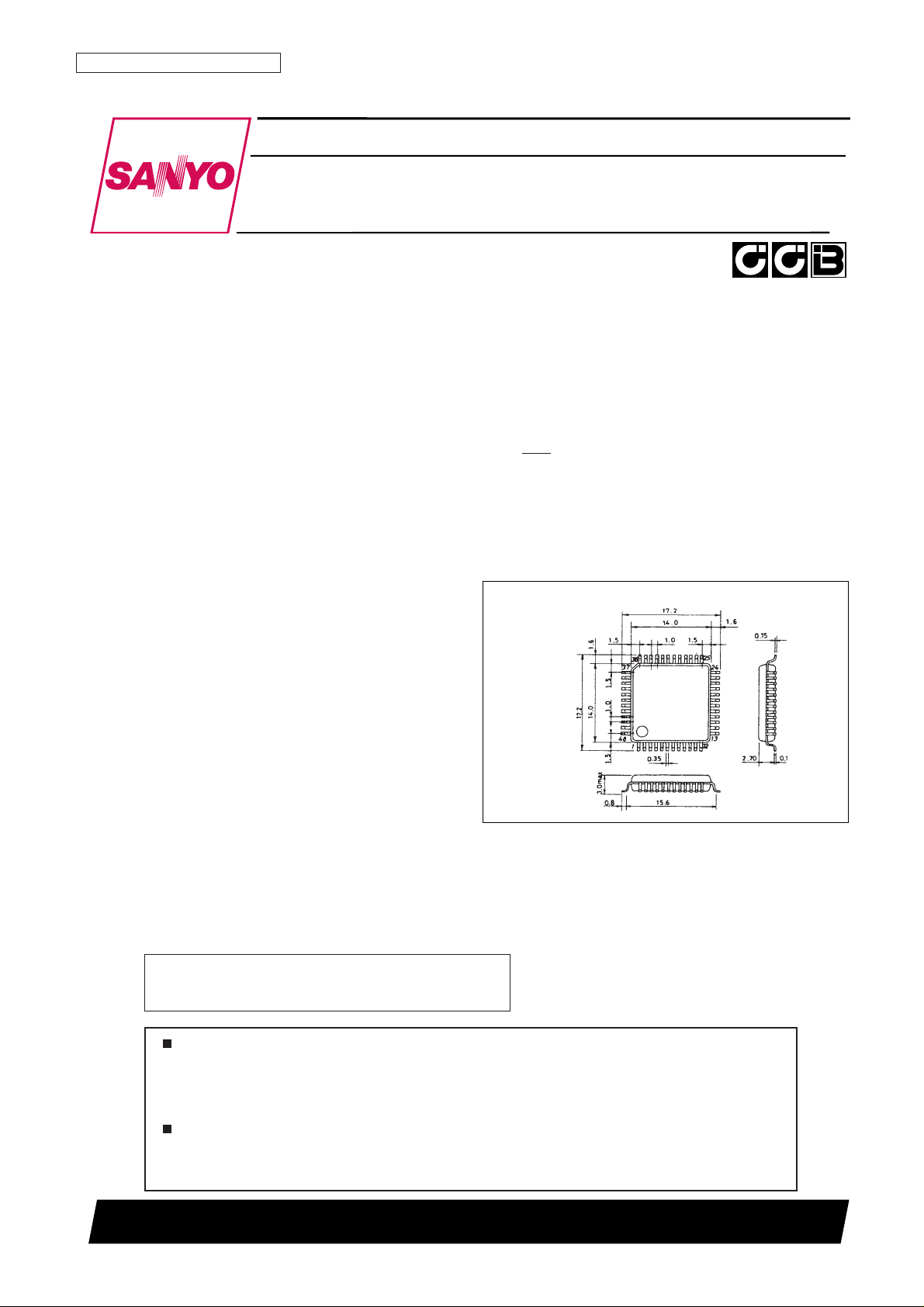
Package Dimensions
unit: mm
3156-QFP48E
• CCB is a trademark of SANYO ELECTRIC CO., LTD.
• CCB is a SANYO’s original bus format and all the
bus addresses are controlled by SANYO.
[LC75834E]
SANYO: QFP48E
Ordering number : EN5597A
93098HA (OT)/63097HA (OT) No. 5597-1/19
1/4 Duty General-Purpose
LCD Drivers
LC75834E, 75834W, 75834JE
SANYO Electric Co.,Ltd. Semiconductor Bussiness Headquarters
TOKYO OFFICE Tokyo Bldg., 1-10, 1 Chome, Ueno, Taito-ku, TOKYO, 110 JAPAN
CMOS LSI
Any and all SANYO products described or contained herein do not have specifications that can handle
applications that require extremely high levels of reliability, such as life-support systems, aircraft’s
control systems, or other applications whose failure can be reasonably expected to result in serious
physical and/or material damage. Consult with your SANYO representative nearest you before using
any SANYO products described or contained herein in such applications.
SANYO assumes no responsibility for equipment failures that result from using products at values that
exceed, even momentarily, rated values (such as maximum ratings, operating condition ranges, or other
parameters) listed in products specifications of any and all SANYO products described or contained
herein.
Continued to next page.
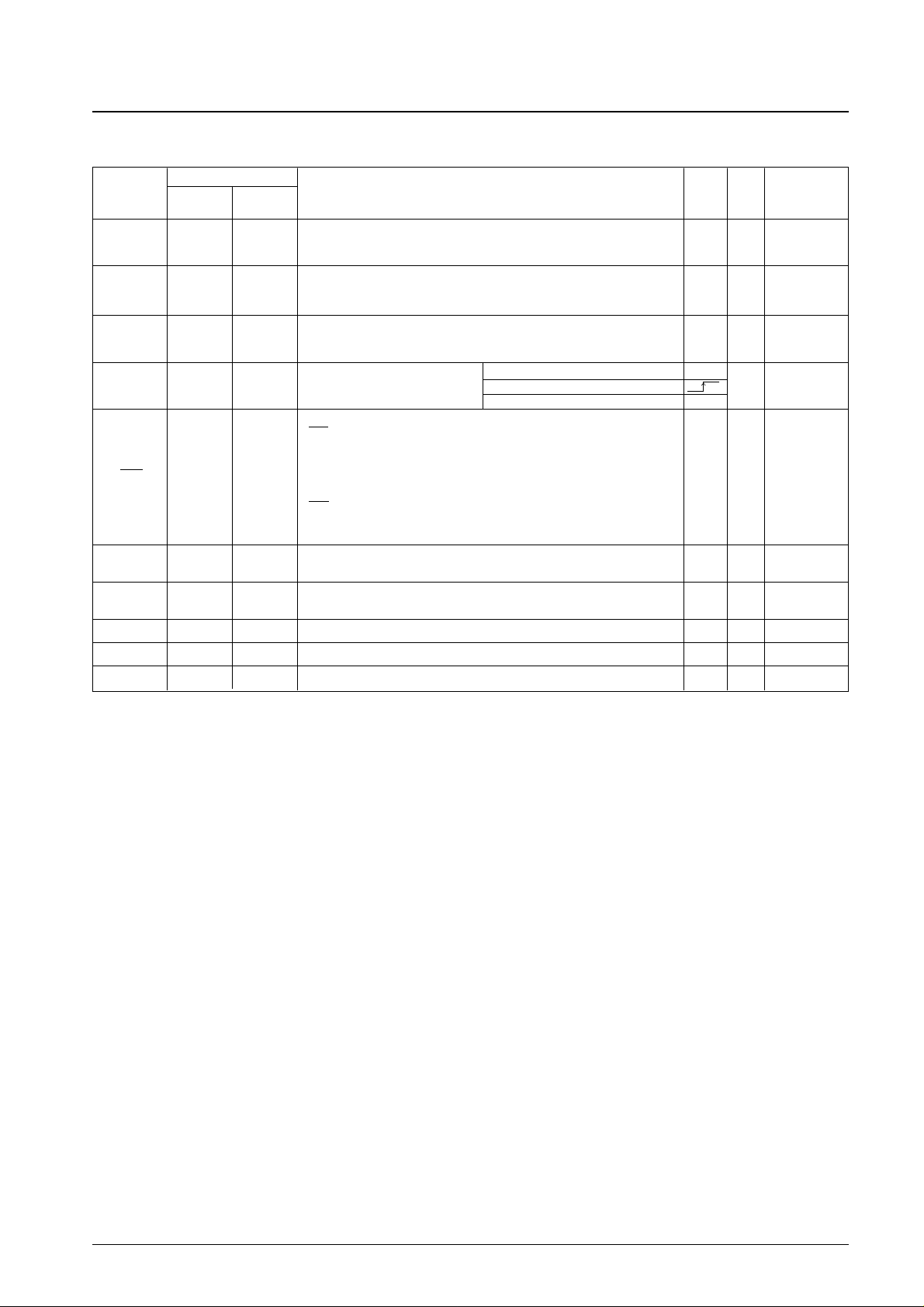
Specifications
Absolute Maximum Ratings at Ta = 25°C, VSS= 0 V
Note: The LC75834JE do not have the S9, S18, S27 S34 output pins.
Allowable Operating Ranges at Ta = –40 to +85°C, VSS= 0 V
No. 5597-2/19
LC75834E, 75834W, 75834JE
Parameter Symbol Conditions Ratings Unit
Maximum supply voltage
V
DD
max V
DD
–0.3 to +7.0 V
V
LCD
max V
LCD
–0.3 to +7.0 V
V
IN
1 CE, CL, DI, INH –0.3 to +7.0 V
Input voltage V
IN
2 OSC –0.3 to VDD+ 0.3 V
V
IN
3 V
LCD
1, V
LCD
2 –0.3 to V
LCD
+ 0.3 V
Output voltage
V
OUT
1 OSC –0.3 to VDD+ 0.3 V
V
OUT
2 S1 to S34, COM1 to COM4, P1 to P8 –0.3 to V
LCD
+ 0.3 V
I
OUT
1 S1 to S34 300 µA
Output current I
OUT
2 COM1 to COM4 3 mA
I
OUT
3 P1 to P8 5 mA
Allowable power dissipation Pd max Ta = 85°C 150 mW
Operating temperature Topr –40 to +85 °C
Storage temperature Tstg –55 to +125 °C
Parameter Symbol Conditions
Ratings
Unit
min typ max
Supply voltage
V
DD
V
DD
2.7 6.0 V
V
LCD
V
LCD
2.7 6.0 V
Input voltage
V
LCD
1 V
LCD
1 2/3 V
LCD
V
LCD
V
V
LCD
2 V
LCD
2 1/3 V
LCD
V
LCD
V
Input high-level voltage V
IH
CE, CL, DI, INH 0.8 V
DD
6.0 V
Input low-level voltage V
IL
CE, CL, DI, INH 0 0.2 V
DD
V
Recommended external resistance R
OSC
OSC 43 kΩ
Recommended external capacitance C
OSC
OSC 680 pF
Guaranteed oscillation range f
OSC
OSC 25 50 100 kHz
Data setup time t
ds
CL, DI: Figure 2 160 ns
Data hold time t
dh
CL, DI: Figure 2 160 ns
CE wait time t
cp
CE, CL: Figure 2 160 ns
CE setup time t
cs
CE, CL: Figure 2 160 ns
CE hold time t
ch
CE, CL: Figure 2 160 ns
High-level clock pulse width t
øH
CL: Figure 2 160 ns
Low-level clock pulse width t
øL
CL: Figure 2 160 ns
Rise time t
r
CE, CL, DI: Figure 2 160 ns
Fall time t
f
CE, CL, DI: Figure 2 160 ns
INH switching time t
c
INH, CE: Figure 3 10 µs
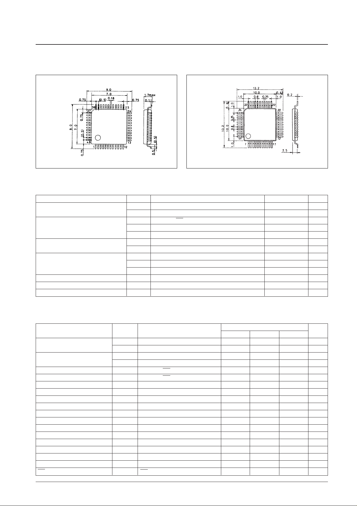
unit: mm
3163A-SQFP48
unit: mm
3148-QFP44MA
[LC75834JE]
SANYO: QIP44MA
[LC75834W]
SANYO: SQFP48
Continued from preceding page.
No. 5597-3/19
LC75834E, 75834W, 75834JE
Electrical Characteristics for the Allowable Operating Ranges
Note: *1 Excluding the bias voltage generation divider resistors built in the V
LCD
1 and V
LCD
2. (See Figure 1.)
The LC75834JE do not have the S9, S18, S27, S34 output pins.
Parameter Symbol Conditions
Ratings
Unit
min typ max
Hysteresis width V
H
CE, CL, DI, INH 0.1 V
DD
V
Input high level current I
IH
CE, CL, DI, INH; VI= 6.0 V 5.0 µA
Input low level current I
IL
CE, CL, DI, INH; VI= 0 V –5.0 µA
V
OH
1 S1 to S34; IO= –20 µA V
LCD
– 0.9 V
Output high-level voltage V
OH
2 COM1 to COM4; IO= –100 µA V
LCD
– 0.9 V
V
OH
3 P1 to P8; IO= –1 mA V
LCD
– 0.9 V
V
OL
1 S1 to S34; IO= 20 µA 0.9 V
Output low-level voltage V
OL
2 COM1 to COM4; IO= 100 µA 0.9 V
V
OL
3 P1 to P8; IO= 1 mA 0.9 V
V
MID
1
COM1 to COM4; 1/2 bias,
1/2 V
LCD
– 0.9 1/2 V
LCD
+ 0.9 V
I
O
= ±100 µA
V
MID
2
S1 to S34; 1/3 bias,
2/3 V
LCD
– 0.9 2/3 V
LCD
+ 0.9 V
I
O
= ±20 µA
Output middle-level voltage*1
V
MID
3
S1 to S34; 1/3 bias,
1/3 V
LCD
– 0.9 1/3 V
LCD
+ 0.9 V
I
O
= ±20 µA
V
MID
4
COM1 to COM4; 1/3 bias,
2/3 V
LCD
– 0.9 2/3 V
LCD
+ 0.9 V
I
O
= ±100 µA
V
MID
5
COM1 to COM4; 1/3 bias,
1/3 V
LCD
– 0.9 1/3 V
LCD
+ 0.9 V
I
O
= ±100 µA
Oscillator frequency f
OSC
OSC; R
OSC
= 43 kΩ C
OSC
= 680 pF 40 50 60 kHz
I
DD
1 VDD; power saving mode 5 µA
I
DD
2 VDD; VDD= 6.0 V, output open, fosc = 50 k Hz 230 460 µA
I
LCD
1 V
LCD
; power saving mode 5 µA
Current drain
I
LCD
2
V
LCD
; V
LCD
= 6.0 V, output open
100 200 µA
1/2 bias, fosc = 50 k Hz
I
LCD
3
V
LCD
; V
LCD
= 6.0 V, output open
60 120 µA
1/3 bias, fosc = 50 k Hz
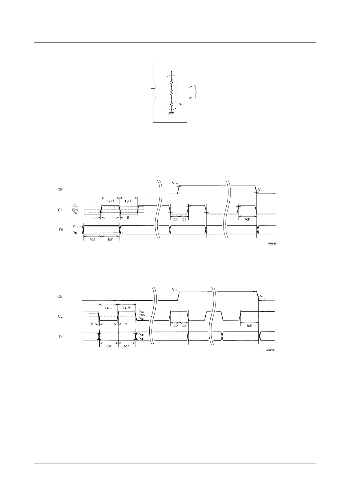
Figure 1
1. When CL is stopped at the low level
2. When CL is stopped at the high level
Figure 2
No. 5597-4/19
LC75834E, 75834W, 75834JE
V
LCD
1
V
LCD
2
V
LCD
V
SS
A06588
To the common segments driver
Except these resistors
s
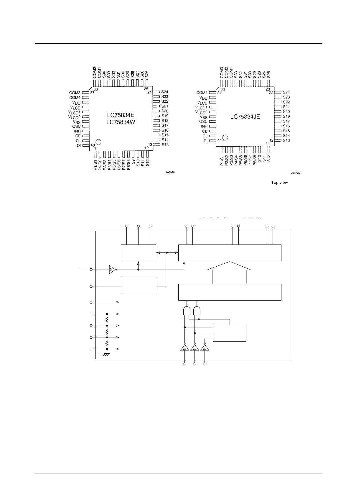
Pin Assignments
Block Diagram
Note: The LC75834JE do not have the S9, S18, S27, S34 output pins.
No. 5597-5/19
LC75834E, 75834W, 75834JE
Common
driver
Address
detector
Clock
generator
Segment driver & latch
Shift register
INH
OSC
V
DD
V
LCD
V
LCD
1
V
LCD
2
V
SS
DI
CL
CE
COM3
COM2
COM1
S35
S34
S9
S8/P8
S2/P2
S1/P1
A06591
Pin Functions
Note: The LC75834JE do not have the S9, S18, S27, S34 output pins.
No. 5597-6/19
LC75834E, 75834W, 75834JE
CE: Chip enable
CL: Synchronization clock
DI: Transfer data
H
—
S1/P1 to
S8/P8
S9 to S34
Pin
1 to 8
9 to 34
LC75834E,
75834W
LC75834JE
1 to 8
9 to 30
— O Open
Segment outputs for displaying the display data transferred by serial data
input. The pins S1/P1 to S8/P8 can be used as general-purpose output ports
when so set up by the control data.
COM1
COM2
COM3
COM4
35
36
37
38
31
32
33
34
— O Open
Common driver outputs.
The frame frequency f
O
is given by: fO= (f
OSC
/512) Hz.
OSC
44 40
CE
CL
DI
46
47
48
42
43
44
Serial data transfer inputs. These
pins are connected to the control
microprocessor.
—
I/O
V
DD
I GND
Oscillator connection
An oscillator circuit is formed by connecting an external resistor and capacitor
V
LCD
1
41 37 — I Open
Used to apply the LCD drive 2/3-bias voltage externally. This pin must be
connected to V
LCD
2 when 1/2-bias drive is used.
V
LCD
2
42 38 — I Open
Used to apply the LCD drive 1/3-bias voltage externally. This pin must be
connected to V
LCD
1 when 1/2-bias drive is used.
V
DD
39 35 — — —Logic block power supply. Provide a voltage in the range 2.7 to 6.0 V.
V
LCD
40 36 — — —LCD driver block power supply. Provide a voltage in the range 2.7 to 6.0 V.
V
SS
43 39 — — —Ground pin. Connect to ground.
INH 45 41 L I GND
Display off control input
•INH = low (V
SS
): Off
S1/P1 to S8/P8 = Low
(These pins are forcible set to the segment output port
function and fixed at the V
SS
level.)
S9 to S34 = Low (V
SS
),
COM1 to COM4 = Low (V
SS
)
•INH = high (V
DD
): On
Note that serial data transfers can be performed when the
display is forced off by this pin.
Active I/O
Handling
when unused
Function
Pin No.
 Loading...