


LC7218M
CMOS LSI
Ordering number : EN4758B
63096HA (OT)/42895TH (OT) No. 4758-1/16
SANYO Electric Co.,Ltd. Semiconductor Bussiness Headquarters
TOKYO OFFICE Tokyo Bldg., 1-10, 1 Chome, Ueno, Taito-ku, TOKYO, 110 JAPAN
PLL Frequency Synthesizer
for Electronic Tuning in AV Systems
LC7218, 7218M, 7218JM
Overview
The LC7218, LC7218M and LC7218JM are PLL
frequency synthesizers for electronic tuning. The LC7218,
LC7218M and LC7218JM are optimal for AM/FM tuner
circuits that require high mounting densities.
Features
• These products feature a rich set of built-in functions for
AV applications, including reference frequency and
unlock detection circuits, I/O ports and a generalpurpose counter.
Functions
• Programmable dividers
— FMIN pin: 130 MHz at 70 mVrms and 160 MHz at
100 mVrms input (built-in prescaler)
— AMIN pin: Pulse swallower and direct division
techniques
• Reference frequencies: Ten selectable frequencies:
1, 5, 9, 10, 3.125, 6.25, 12.5 25, 50 and 100 kHz
• Output ports: 7 pins
Complementary outputs: 2 pins
N-channel open drain outputs: 5 pins
• Input ports: 2 pins
• General-purpose counter: For measuring IF and other
signals (Also used for station detection when
functioning as an IF counter.)
— HCTR pin: Frequency measurement (for inputs up
to 70 MHz)
— LCTR pin: Frequency and period measurement
• PLL unlock detection circuit
Detects phase differences of 0.55, 1.11, 2.22 and 3.33 µs.
• Controller clock output: 400 kHz
• Clock time base output: 8 Hz
• Serial data I/O
— Supports CCB format communication with the
system controller.
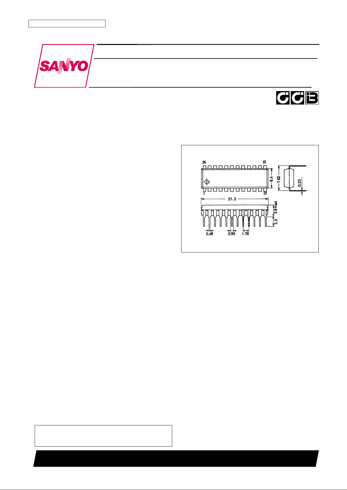
• Package: LC7218: DIP24S
LC7218M: MFP24
LC7218JM: MFP24S
Package Dimensions
unit: mm
3067-DIP24S
SANYO: DIP24S
[LC7218]
• CCB is a trademark of SANYO ELECTRIC CO., LTD.
• CCB is SANYO’s original bus format and all the bus
addresses are controlled by SANYO.
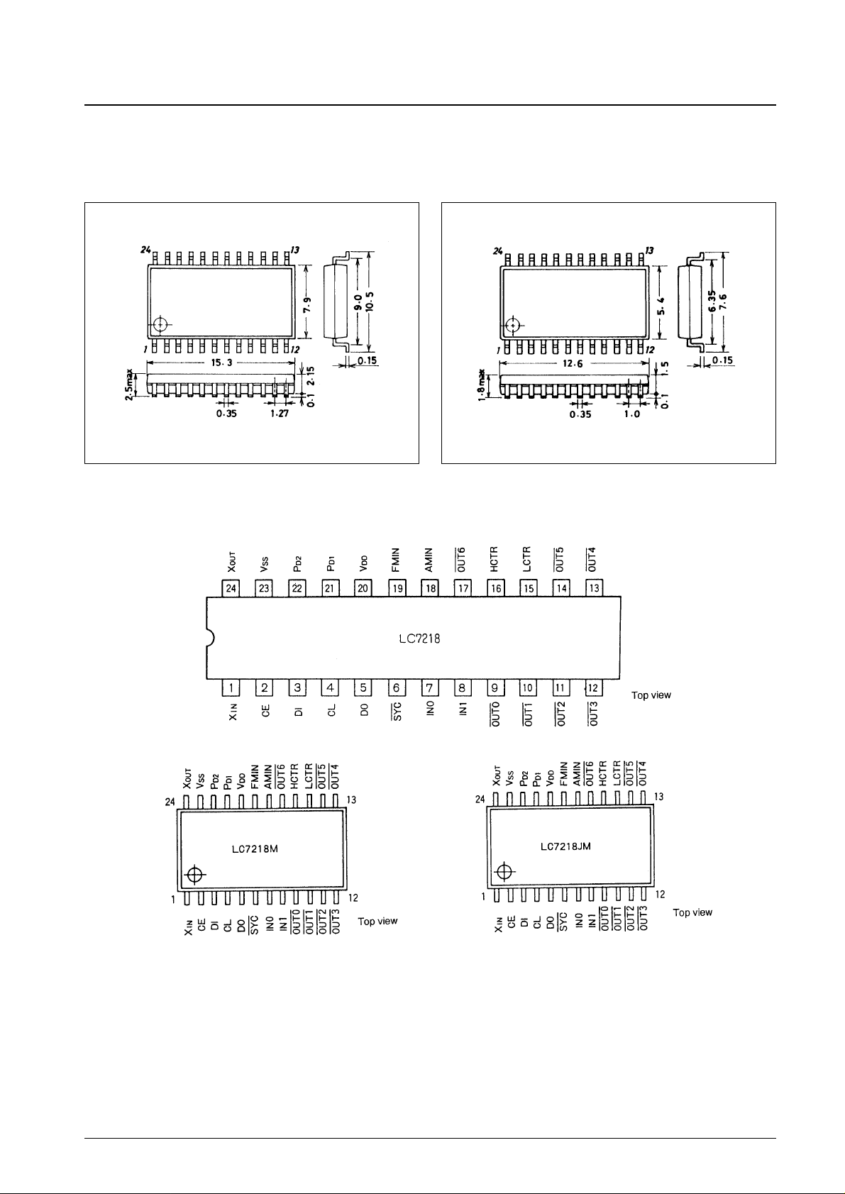
Package Dimensions
unit: mm unit: mm
3045B-MFP24 3112-MFP24S
Pin Assignments
No. 4758-2/16
LC7218, 7218M, 7218JM
SANYO: MFP24
[LC7218M]
SANYO: MFP24S
[LC7218JM]
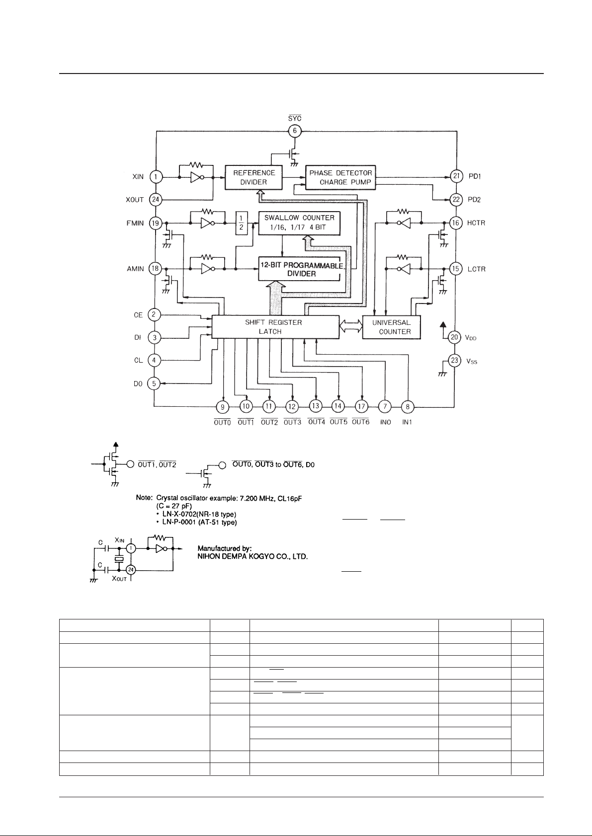
Block Diagram
Pin Symbols
XIN, XOUT: Crystal oscillator (7.2 MHz)
FMIN, AMIN: Local oscillator signal input
CE, CL, DI, DO: Serial data I/O
OUT0 to OUT6: Output ports
IN0, IN1: Input ports
HCTR, LCTR: General-purpose counter inputs
PD1, PD2: Charge pump outputs
SYC: Control clock (400 kHz)
Specifications
Absolute Maximum Ratings at Ta = 25°C, VSS= 0 V
No. 4758-3/16
LC7218, 7218M, 7218JM
Parameter Symbol Conditions Ratings Unit
Maximum supply voltage V
DD
max V
DD
–0.3 to +7.0 V
Input voltage
V
IN
(1) CE, CL, DI, IN0, IN1 –0.3 to +7.0 V
V
IN
(2) Input pins other than VIN(1) –0.3 to VDD+ 0.3 V
V
OUT
(1) DO, SYC –0.3 to +7.0 V
Output voltage
V
OUT
(2) OUT1, OUT2 –0.3 to VDD+ 0.3 V
V
OUT
(3) OUT3 to OUT6, OUT0 –0.3 to +15 V
V
OUT
(4) Output pins other than V
OUT
(1), V
OUT
(2) and V
OUT
(3) –0.3 to VDD+ 0.3 V
Ta ≤ 85°C :LC7218 350
Allowable power dissipation Pd max :LC7218M 300 mW
:LC7218JM 200
Operating temperature Topr –40 to +85 °C
Storage temperature Tstg –55 to +125 °C
Allowable Operating Ranges at Ta = –40 to +85°C, VSS= 0 V
Note: 1.
DV and SP are bits in the serial data.
*: don’t care
2. Frequency measurement
3. Frequency measurement
4. Period measurement
5. f
IN
(2): 10 to 160 MHz/VIN(2)
0.100 Vrms (minimum)
6. f
IN
(4): 10 to 70 MHz/VIN(4)
0.100 Vrms (minimum)
No. 4758-4/16
LC7218, 7218M, 7218JM
Parameter Symbol Conditions min typ max Unit
Supply voltage
V
DD
(1) V
DD
4.5 6.5 V
V
DD
(2) VDD: Crystal oscillator guaranteed operation 3.5 6.5 V
Input high level voltage
V
IH
(1) CE, CL, DI, IN0, IN1 2.2 6.5 V
V
IH
(2) LCTR: Pulse waveform, DC coupling
*4
0.7 VDD(1) VDD(1) V
Input low level voltage
V
IL
(1) CE, CL, DI, IN0, IN1 0 0.7 V
V
IL
(2) LCTR
*4
0 0.3 VDD(1) V
Output voltage
V
OUT
(1) DO, SYC 6.5 V
V
OUT
(2) OUT3 to OUT6, OUT0 13 V
f
IN
(1) XIN: Sine wave capacitor coupling, VDD(2) 1.0 7.2 8.0 MHz
f
IN
(2) FMIN: Sine wave capacitor coupling, VDD(1)
*1
10 130 (160)*5MHz
Input frequency
f
IN
(3) AMIN: Sine wave capacitor coupling, VDD(1)
*1
0.5 40 MHz
f
IN
(4) HCTR: Sine wave capacitor coupling, VDD(1)
*2
10 60 (70)*6MHz
f
IN
(5) LCTR: Sine wave capacitor coupling, VDD(1)
*3
15 500 kHz
f
IN
(6) LCTR: Pulse wave DC coupling, VDD(1)
*4
1.0 20 × 103Hz
Crystal oscillators for which
Xtal X
IN-XOUT
: CI ≤ 50 Ω 3.0 7.2 8.0 MHz
operation is guaranteed
V
IN
(1) XIN: Sine wave capacitor coupling, VDD(1) 0.5 1.5 Vrms
V
IN
(2) FMIN: Sine wave capacitor coupling, VDD(1)
0.070
1.5 Vrms
(0.100)
*5
Input amplitude VIN(3) AMIN: Sine wave capacitor coupling, VDD(1) 0.070 1.5 Vrms
V
IN
(4) HCTR: Sine wave capacitor coupling, VDD(1)
*2
0.070
1.5 Vrms
(0.100)
*6
VIN(5) LCTR: Sine wave capacitor coupling, VDD(1)
*3
0.070 1.5 Vrms
DV SP Input frequency 1/2 divider 1/16, 17 swallow 12-bit main divider Input pin
1 * 10 to 130 (160) MHz
●● ●● ●● FMIN
0 1 2 to 40 MHz —
●● ●● AMIN
0 0 0.5 to 10 MHz — —
●● AMIN
Electrical Characteristics for the Allowable Operating Ranges
Note: A capacitor of at least 2000 pF must be inserted between the power supply VDDand VSSpotentials.
No. 4758-5/16
LC7218, 7218M, 7218JM
Parameter Symbol Conditions min typ max Unit
Rf (1) XIN 1.0 MΩ
Rf (2) FMIN 500 kΩ
Internal feedback resistance Rf (3) AMIN 500 kΩ
Rf (4) HCTR 500 kΩ
Rf (5) LCTR 500 kΩ
Hysteresis V
H
LCTR 0.1 V
DD
0.6 V
DD
V
I
IH
(1) CE, CL, DI: VI= 6.5 V 5.0 µA
I
IH
(2) IN0, IN1: VI= V
DD
5.0 µA
Input high level current I
IH
(3) XIN: VI= V
DD
20 µA
I
IH
(4) FMIN, AMIN: VI= V
DD
40 µA
I
IH
(5) HCTR, LCTR: VI= V
DD
40 µA
I
IL
(1) CE, CL, DI: VI= V
SS
5.0 µA
I
IL
(2) IN0, IN1: VI= V
SS
5.0 µA
Input low level current I
IL
(3) XIN: VI= V
SS
20 µA
I
IL
(4) FMIN, AMIN: VI= V
SS
40 µA
I
IL
(5) HCTR, LCTR: VI= V
SS
40 µA
Output high level voltage
V
OH
(1) OUT1, OUT2: IO= –1 mA VDD– 1.0 V
V
OH
(2) PD1, PD2: IO= –0.5 mA VDD– 1.0 V
V
OL
(1) OUT1, OUT2: IO= 1 mA 1.0 V
V
OL
(2) PD1, PD2: IO= 0.5 mA 1.0 V
Output low level voltage
V
OL
(3) OUT3 to OUT6: IO= 5 mA 1.0 V
V
OL
(4) OUT0: IO= 1 mA 1.0 V
V
OL
(5) DO: IO= 5 mA 1.0 V
V
OL
(6) SYC: IO= 0.5 mA (VDD= 3.5 to 6.5 V) 1.0 V
I
OFF
(1) OUT3 to OUT6, OUT0: VO= 13 V 5.0 µA
Output off leakage current I
OFF
(2) DO: VO= 6.5 V 5.0 µA
I
OFF
(3) SYC: VO= 6.5 V (VDD= 3.5 to 6.5 V) 5.0 µA
Three-state high level
I
OFFH
PD1, PD2: VO= V
DD
0.01 10.0 nA
off leakage current
Three-state low level
I
OFFL
PD1, PD2: VO= V
SS
0.01 10.0 nA
off leakage current
Input capacitance C
IN
FMIN, HCTR 1 2 3 pF
V
DD
: fIN(2) = 130 MHz, VIN(2) = 70 mVrms,
I
DD
(1) with a 7.2 MHz crystal, other input pins at VSS, 20 30 mA
Current drain
output pins open
VDD: PLL block stopped (PLL inhibit state), crystal
I
DD
(2) oscillator operating (SYC, TB), with a 7.2 MHz crystal, 1.0 mA
other input pins at V
SS
, output pins open
 Loading...