


Ordering number:ENN3942
CMOS IC
LC7536LHS
High-Voltage, Two-Channel
Electronic Attenuator
Overview
The LC7536LHS is a two-channel electronic attenuator for volume, balance and loudness controls in stereo audio applications.
The LC7536LHS reads data from a three-line serial bus to control attenuation in 1 dB steps over an 80 dB range, up to a maximum of 96 dB. It features a center tap at 20 dB attenuation for a loudness control using a minimum of external components. A device select pin allows two devices to be connected to the serial bus.
The LC7536LHS operates from 5 V and 10 V supplies and is available in 30-pin DIPs.
Features
•Three-line serial control.
•Two device select.
•Tap at 20 dB attenuation for a loudness control.
•80 dB attenuation range adjustable in 1 dB steps.
•96 dB maximum attenuation.
•75 dB crosstalk rejection.
•0.022% total harmonic distortion.
•47kΩ input impedance.
•5 V and 10 V supplies.
•30-pin DIP.
Package Dimensions
unit:mm |
|
|
|
|
|
3061-DIP30S |
|
|
|
|
|
|
|
|
[LC7536LHS] |
|
|
|
30 |
|
|
16 |
|
|
|
|
|
10.16 |
8.6 |
|
|
|
|
|
0.25 |
|
1 |
|
|
15 |
|
|
|
27.2 |
|
|
|
|
|
|
|
4.25 |
4.95max |
|
|
|
|
|
3.2 |
1.15 |
1.78 |
0.48 |
0.95 |
0.51min |
|
|
|
|
|
|
|
|
|
|
|
SANYO : DIP30S |
|
Specifications
Absolute Maximum Ratings at Ta=25˚C, VSS=0V, VEE=0V
Parameter |
Symbol |
Conditions |
Ratings |
Unit |
|
|
|
|
|
Maximum supply voltage |
VDD max |
|
0 to 12 |
V |
VCC max |
|
0 to 7 |
||
|
|
|
||
CLK, DI and CE input voltage range |
VI1 |
|
0 to VCC+0.3 |
V |
Analog input voltage range |
VI2 |
|
VEE–0.3 |
V |
|
|
|
to VDD+0.3 |
|
Select pin input voltage range |
VI3 |
|
VCC–0.3 |
V |
|
|
|
to VDD+0.3 |
|
Allowable power dissipation |
Pd max |
Ta≤85°C |
250 |
mW |
Operating temperature range |
Topr |
|
–40 to +85 |
˚C |
Stroage temperature range |
Tstg |
|
–50 to +125 |
˚C |
 Any and all SANYO products described or contained herein do not have specifications that can handle applications that require extremely high levels of reliability, such as life-support systems, aircraft’s control systems, or other applications whose failure can be reasonably expected to result in serious physical and/or material damage. Consult with your SANYO representative nearest you before using any SANYO products described or contained herein in such applications.
 SANYO assumes no responsibility for equipment failures that result from using products at values that exceed, even momentarily, rated values (such as maximum ratings, operating condition ranges,or other parameters) listed in products specifications of any and all SANYO products described or contained herein.
SANYO Electric Co.,Ltd. Semiconductor Company
TOKYO OFFICE Tokyo Bldg., 1-10, 1 Chome, Ueno, Taito-ku, TOKYO, 110-8534 JAPAN
51501TN (KT)/8051JN No.3942–1/7
LC7536LHS
Recommended Operating Conditions at Ta = 25˚C, VSS = 0 V, VEE = 0 V
Parameter |
Symbol |
Conditions |
Ratings |
Unit |
|
|
|
|
|
Analog supply voltage |
VDD |
|
VCC+3.2 to 10.0 |
V |
Logic supply voltage |
VCC |
|
5 |
V |
Logic supply voltage |
VCC |
|
3.6 to 5.5 |
V |
Electrical Characteristics at Ta = 25˚C, VCC = 5 V, VDD = 10 V, VEE = 0 V, VSS = 0 V
Parameter |
Symbol |
Conditions |
|
Ratings |
|
Unit |
|
|
|
||||
|
|
|
min |
typ |
max |
|
|
|
|
|
|
|
|
Supply current |
IDD |
|
|
|
1 |
mA |
ICC |
|
|
|
1 |
||
|
|
|
|
|
||
Serial bus HIGH-level input voltage |
VIH1 |
|
0.8VCC |
|
VCC |
V |
|
|
|
0.8× |
|
|
|
Select pin HIGH-level input voltage |
VIH2 |
|
(VDD |
|
VDD |
V |
|
–VCC) |
|
||||
|
|
|
+VCC |
|
|
|
Serial bus LOW-level input voltage |
VIL1 |
|
VSS |
|
0.2VCC |
V |
|
|
|
|
|
0.2× |
|
Select pin LOW-level input voltage |
VIL2 |
|
VCC |
|
(VDD |
V |
|
|
–VCC) |
||||
|
|
|
|
|
+VCC |
|
Input voltage |
VIN |
|
VEE |
|
VDD |
VP-P |
Input pulsewidth |
tΦW |
|
20 |
|
|
µs |
Setup time |
tsetup |
|
20 |
|
|
µs |
Hold time |
thold |
|
20 |
|
|
µs |
Operating frequency |
fopg |
|
|
|
25 |
kHz |
Output leakage current |
IOFF |
Analog switches OFF |
–10 |
|
+10 |
µA |
Total harmonic distortion |
THD |
VIN=0.3V, f=1kHz, VDD–VEE=10V, |
|
0.022 |
|
% |
|
|
VR=VR(max) |
|
|
|
|
Crosstalk rejection |
Cr |
f=20kHz, VIN=1V |
60 |
75 |
|
dB |
Maximum attenuation |
V0 |
f=20kHz, VIN=1V |
|
96 |
|
dB |
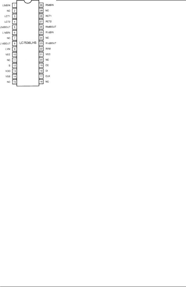
Pin Assignment
Top view
No.3942–2/7

LC7536LHS
Block Diagram
Pin Description
Number |
Name |
Description |
|
|
|
|
|
1 |
L5dBIN |
Left-channel 5 dB attenutaiton step input. Low-impedance drive. 75 kΩ total resistance. |
|
|
|
|
|
2 |
NC |
No connection |
|
|
|
|
|
3 |
LCT1 |
Left-channel loudness compensation inputs. |
|
|
|
||
4 |
LCT2 |
||
|
|||
|
|
|
|
5 |
L5dBOUT |
Left-channel 5 dB attenutaiton step output. Approximately 1 MΩ load resistance. |
|
|
|
|
|
6 |
L1dBIN |
Left-channel 1 dB attenutaiton step input. Low-impedance drive. |
|
|
|
|
|
7 |
NC |
No connection |
|
|
|
|
|
8 |
L1dBOUT |
Left-channel 1 dB attenutaiton step output. 47 kΩ to 1 MΩ load resistance. |
|
|
|
|
|
9 |
LVM |
Left-channel volume control common. Normally connected to ground. |
|
|
|
|
|
10 |
VEE |
Ground |
|
11 |
NC |
No connection |
|
|
|
|
|
12 |
S |
Address select input. |
|
|
|
|
|
13 |
VDD |
10 V supply |
|
14 |
VSS |
Ground |
|
15 |
NC |
No connection |
|
|
|
||
16 |
NC |
||
|
|||
|
|
|
|
17 |
CLK |
Clock input. |
|
|
|
|
|
18 |
D1 |
Serial data input. |
|
|
|
|
|
19 |
CE |
Chip enable input. |
|
|
|
|
|
20 |
NC |
No connection |
|
|
|
|
|
21 |
VCC |
5 V supply |
|
22 |
RVM |
Right-channel volume control common. Normally connected to ground. |
|
|
|
|
|
23 |
R1dBOUT |
Right-channel 1 dB attenutaiton step otuput. 47 kΩ to 1 MΩ load resistance. |
|
|
|
|
|
24 |
NC |
No connection |
|
|
|
|
|
25 |
R1dBIN |
Right-channel 1 dB attenutaiton step input. Low-impedance drive. |
|
|
|
|
|
26 |
R5dBOUT |
Right-channel 5 dB attenutaiton step output. Approximately 1 MΩ load resistance. |
|
|
|
|
|
27 |
RCT2 |
Right-channel loudness compensation inputs. |
|
|
|
||
28 |
RCT1 |
||
|
|||
|
|
|
|
29 |
NC |
No connection |
|
|
|
|
|
30 |
R5dBIN |
Right-channel 5 dB attenutaiton step input. Low-impedance drive. 75 kΩ total resistance. |
|
|
|
|
No.3942–3/7
 Loading...