


Ordering number : EN1506D
Monolithic Linear IC
LA1260
FM/AM Tuner System for Radio-Casette Recorders, Music Centers
Functions |
Package Dimensions |
|
FM : IF amplifier, quadrature detector, AF preamplifier, |
unit : mm |
|
|
||
tuning indicator drive output. |
3006B-DIP16 |
|
AM : RF amplifier, MIX, OSC (with ALC), IF amplifier, |
||
|
||
Detector, AGC, tuning indicator drive. |
[LA1260] |
Features
•Minimum number of external parts required (No AM detection coil required).
•High S/N : FM 81dB
AM 53dB
• Low-level AM oscillator with ALC : Pin 16 OSC output
MW 130mV DIP16 SW 70 mV to 90 mV
(7MHz) (24MHz)
•Less AM whistle interference : Whistle 1% at input 100dB/m.
•On-chip LED tuning indicator driver.
•On-chip FM/AM selector.
•Independent FM/AM output pins : Possible to set FM/AM frequency characteristic independently.
Specifications
Maximum Ratings at Ta=25°C, See specified Test Circuit.
Parameter |
Symbol |
Conditions |
Ratings |
Unit |
Maximum supply voltage |
VCC max |
Pins 6, 12 |
9 |
V |
Maximum current drain |
ICC max |
Pins 6+7+12 |
50 |
mA |
Flow-in current |
I7 |
Pin 7 |
20 |
mA |
Flow-out current |
I15 |
Pin 15 |
0.1 |
mA |
Allowable power dissipation |
Pd max |
Ta≤ 70°C |
450 |
mW |
Operating temperature |
Topr |
|
–20 to +70 |
°C |
|
|
|
|
|
Storage temperature |
Tstg |
|
–40 to +125 |
°C |
|
|
|
|
|
Operating Conditions at Ta=25°C
Parameter |
Symbol |
Conditions |
Ratings |
Unit |
|
|
|
|
|
Recommended operating voltage |
VCC |
|
4.5 |
V |
Operating voltage range |
VCC op |
|
3.0 to 8.0 |
V |
SANYO Electric Co.,Ltd. Semiconductor Bussiness Headquarters
TOKYO OFFICE Tokyo Bldg., 1-10, 1 Chome, Ueno, Taito-ku, TOKYO, 110 JAPAN
N2897HA (KT)/33194HO/O067KI/8225MW/4045KI/8084KI, TS No.1506-1/14

LA1260
Operating Characteristics at Ta=25°C, VCC=4.5V, See specified Test Circuit
Parameter |
Symbol |
Conditions |
|
Ratings |
|
Unit |
|
min |
typ |
|
max |
||||
|
|
|
|
|
|||
|
|
|
|
|
|
|
|
[AM Characteristics : f=1MHz] |
|
|
|
|
|
|
|
|
|
|
|
|
|
|
|
Quiescent current |
Icco AM |
VIN=No input |
|
7.5 |
|
10.5 |
mA |
Detection output |
VO1 |
VIN=23dBµ, 400Hz-30% mod. |
–33 |
–28 |
|
–23 |
dBm |
|
|
|
17.3 |
31 |
|
55 |
mV |
|
|
|
|
|
|
|
|
S/N ratio |
S/N1 |
VIN=23dBµ, 400Hz-30% mod. |
18.0 |
21.5 |
|
|
dB |
Detection output |
VO2 |
VIN=60dBµ, 400Hz-30% mod. |
–19.0 |
–16.0 |
|
–13.0 |
dBm |
|
|
|
87 |
122 |
|
174 |
mV |
|
|
|
|
|
|
|
|
S/N ratio |
S/N2 |
VIN=60dBµ, 400Hz-30% mod. |
48 |
53 |
|
|
dB |
Total harmonic distortion |
THD1 |
VIN=60dBµ, 400Hz-30% mod. |
|
0.45 |
|
1.3 |
% |
|
THD2 |
VIN=100dBµ, 400Hz-30% mod. |
|
1.5 |
|
3.0 |
% |
LED lighting voltage |
VLEDAM |
IC=1mA |
22 |
30 |
|
38 |
dBm |
Oscillation output (24MHz) |
VOSC24M |
|
60 |
86 |
|
120 |
mV |
[FM Characteristics : f=10.7MHz] |
|
|
|
|
|
|
|
|
|
|
|
|
|
|
|
Quiescent current |
IccoFM |
VIN=No input |
|
8.5 |
|
12.0 |
mA |
–3dB sensitivity |
VINlim |
–3dB down, 400Hz-100% mod. |
|
35 |
|
42 |
dBµ |
Demodulation output |
VO3 |
VIN=80dBµ, 400Hz-100% mod. |
–12.5 |
–9.5 |
|
–6.5 |
dBm |
|
|
|
183 |
260 |
|
367 |
mV |
|
|
|
|
|
|
|
|
S/N ratio |
S/N3 |
VIN=80dBµ, 400Hz-100% mod. |
77 |
81 |
|
|
dB |
|
S/N4 |
VIN=80dBµ, 400Hz-30% mod. |
|
71 |
|
|
dB |
Total harmonic distortion |
THD3 |
VIN=80dBµ, 400Hz-100% mod. |
|
0.55 |
|
1.2 |
% |
|
THD4 |
VIN=80dBµ, 400Hz-30% mod. |
|
0.05 |
|
|
% |
LED lighting voltage |
VLEDFM |
IL=1mA |
|
39 |
|
49 |
dBµ |
AM rejection ratio |
AMR |
VIN=80dBµ, 400Hz-100% FM mod. |
|
60 |
|
|
dB |
|
|
1kHz-30% AM mod. |
|
|
|
|
|
|
|
|
|
|
|
|
|
Equivalent Circuit Block Diagram
No.1506-2/14

LA1260
Test Circuit
Unit (resistance : Ω , capacitance : F)
T1 Mitsumi YT30194 (56pF tuning)
T2 Mitsumi KW30011
T3 Mitsumi YT30105
T4 Mitsumi YT30112
Proper Cares in Using the IC
External parts placement and pattern
•The AM local oscillation parts, AM local oscillation coil, and antenna circuit parts such as bar antenna must be separated from each other as far as possible to prevent Qs from worsening.
•Pin 16 (AM oscillation injection pin) and pin 14 (RF input pin) must be separated from each other on the pattern as shown in Figure. A below. Care should be taken not to make unwanted coupling by parallel wiring as shown in Figure B to prevent Qs from worsening.
Figure A Good example Figure B Bad example
FM quadrature detection coil
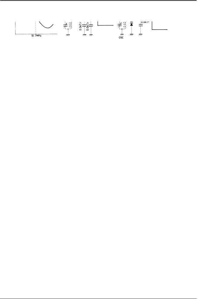
• The values recommended for the detection coil are shown below. (See Figure 1.)
Tuning capacitance |
: 56pF |
|
|
Damping resistance |
: 6.8kΩ |
|
|
• Values other than recommended provide the LED drive characteristic as shown below. |
|||
|
|
|
|
|
Value increased |
Value decreased |
|
|
|
|
|
Tuning capacitance |
• Lighting is delayed. |
• Lighting is advanced. |
|
|
• No lighting may occur at low |
• Mislighting may occur in the |
|
|
temperature. |
absence of signal. |
|
|
|
|
|
Damping resistance |
• Lighting is advanced. |
• Lighting is delayed. |
|
|
• Mislighting may occur in the |
• No lighting may occur at low |
|
|
absence of signal. |
temperature. |
|
|
|
|
|
If the product of tuning capacitance and damping resistance is equal to that of values recommended above (e. g. tuning capacitance=82pF, damping resistance=4.7kΩ ), other characteristics (demodulation output, S/N, THD, etc.) than the LED drive characteristic remain almost unaffected.
• For applications where a double tuning coil is used, refer to "Applications where a double coil is used" on page 13.
No.1506-3/14
LA1260
How to apply FM AFC
The S curve at the FM output pin (pin 8) is as shown in Figure 1. Therefore, the domestic (Japan) band (lower local oscillation) use and foreign band (upper local oscillation) use differ as shown in Figures 2 and 3.
Figure 1 |
Figure 2 Domestic (lower local |
|
oscillation) band |
Figure 3 Foreign (upper local oscillation) band
Unit (resistance : Ω , capacitance : F)
AM local oscillation
Since the LA1260 contains an ALC circuit, the oscillation level at pin 16 can be limited to 60 to 150mV in the following applications where a coil is used.
Unit (capacitance : F)
Stable oscillation occurs at a coil impedance of 5kΩ or greater viewed from across pins 16 and 15. Turn ratio n and QO must be determined so that the oscillation level at pin 16 becomes 75mV or greater for MW use and 60mV or greater for SW use.
If turn ratio n is increased more than needed, the oscillation level at pin 16 drops, thereby lowering the maximum sensitivity as shown in Figure 5 and 6. Figure 7 shows the relation between turn ratio n and oscillation level at pin 16 in the MW band.
Unit (capacitance : F)
Figure 4
|
dB/m |
S |
– |
V |
|
Maximum sensitivity, |
S |
Usable sensitivity, Q |
Figure 5
21MHz reception mode
Maximum sensitivity (input at detection output –30dBm)
Usable sensitivity (S/N=20dB)
|
dB/m |
S |
– |
V |
|
Maximum sensitivity, |
S |
Usable sensitivity, Q |
Figure 6
fr=1000kHz reception
Usable sensitivity (S/N=20dB)
Maximum sensitivity (input at detection output –30dBm)
OSC injection voltage at pin 16 – mV |
OSC injection voltage at pin 16 – mV |
No.1506-4/14

LA1260
|
|
|
|
|
Figure 7 |
|
||||
|
|
|
|
|
|
|
|
|
|
|
mV |
|
|
|
MW OSC characteristic |
|
|||||
|
|
|
|
|
|
|
|
|
|
|
|
|
|
|
|
|
|
|
|
|
|
– |
|
|
|
|
|
|
|
|
|
|
OSC |
|
|
|
|
|
|||||
|
|
Relation between turn |
|
|||||||
V |
|
|
ration n and OSC level |
|
|
|
|
|
||
OSC voltage at coil end, |
|
|
|
|
||||||
|
|
|
|
|
|
|
|
|||
|
|
|
|
|
|
|
|
|
|
|
OSC voltage at coil end |
|
|
|
|
|
|
|
|
OSC voltage – mV |
|
|
|
|
|
|
V16 OSC voltage |
|
||||
|
|
|
|
|
|
|
|
|
||
|
|
|
|
|
|
|
|
|
|
|
|
|
Receiving frequency, fr – Hz |
V16 |
|||||||
AM oscillation coil
Generally speaking, the following should be noted. Winding with loose coupling between 1 and 2 and between 1 and 3 must be avoided. (Particularly SW1, SW2).
To put in concretely, the pot core type is better than the screw core type which is loose in coupling. This prevents the local oscillation frequency from turning third resonance frequency related to the coupling coefficient.
Unit (capacitance : F)
LED unlighted time and distortion in AM (MW)
By increasing the value of the electrolytic capacitor for AGC at pin 11 (Figure 8), the distortion in the AM mode can be improved, but the LED unlighted time is made longer. 10µ F is recommended for obtaining the optimum LED unlighted time and distortion. The LED unlighted time is 200ms at this value (Approximately 400ms at 22µ F).
FM-AM selection and dc level at pin 12
(1)Pin 12-used method=recommended circuit
The FM mode is entered with pin 12 open. When pin 12 and pin 6 are at the same potential in terms of DC, the AM circuit is turned on by the internal switch. It should be noted that the dynamic range is narrowed whether the potential at pin 12 is lower or high than that at pin 6.
(2)Pin 13-used method
The AM mode is entered with pin 13 open. When pin 13 is grounded, the FM circuit is turned on and the AM circuit is turned off by the internal switch. In this case, pin 12 and pin 6 (VCC) are at the same potential.
Total harmonic distortion, THD – %
Figure 8
Input 100dBm
VCC=4.5V
AM mod. char. and electrolytic capacitor at pin 11.
|
|
|
|
|
|
F |
|
|
|
|
|
|
µ |
|
|
|
|
|
|
10 |
|
|
|
|
|
|
: |
|
|
|
|
|
and |
Gnd |
|
|
|
|
11 |
|
|
|
|
|
pin |
|
|
|
|
|
across |
|
|
|
|
|
capacitor |
|
|
|
|
|
100Hz, |
|
|
|
|
|
|
|
|
|
|
|
|
Unit (capacitance : F)
Modulation degree – %
No.1506-5/14
 Loading...