


LA1787M
Any and all SANYO products described or contained herein do not have specifications that can handle
applications that require extremely high levels of reliability, such as life-support systems, aircraft’s
control systems, or other applications whose failure can be reasonably expected to result in serious
physical and/or material damage. Consult with your SANYO representative nearest you before using
any SANYO products described or contained herein in such applications.
SANYO assumes no responsibility for equipment failures that result from using products at values that
exceed, even momentarily, rated values (such as maximum ratings, operating condition ranges, or other
parameters) listed in products specifications of any and all SANYO products described or contained
herein.
Overview
The LA1787M integrates all six blocks required in a car
radio tuner on a single chip.
Functions
• FM front end
• FM IF
• Noise canceller
• Multiplex
• AM up-conversion
• FM/AM switch
• MRC
Features
• Improved noise reduction methods
— The FM front end provides excellent 3-signal
characteristics equivalent to those of the LA1193M.
— Superlative listenability due to improved medium and
weak field noise canceller characteristics.
— Improved separation characteristics
— Anti-birdie filter
— Improved AM and FM thermal characteristics
— Excellent FM signal meter linearity
— Modified N.C. circuit for improved noise rejection
• Improved AM adjacent channel interference
characteristics (∆40 kHz)
• Double conversion AM tuner (up conversion)
Reduces the number of external components required as
compared to earlier double conversion tuners, in
particular, no crystal is required (when used in
conjunction with the LC72144).
• Sample-to-sample variation reduction circuit built into
the FM IF circuit.
(Fixed resistors are used for the SD, keyed AGC, mute
on adjustment, ATT, SNC, and HCC functions.)
• Improved FM separation temperature characteristics
• The LA1787 inherits the block arrangement of the
LA1780M and supports pin-compatible designs.
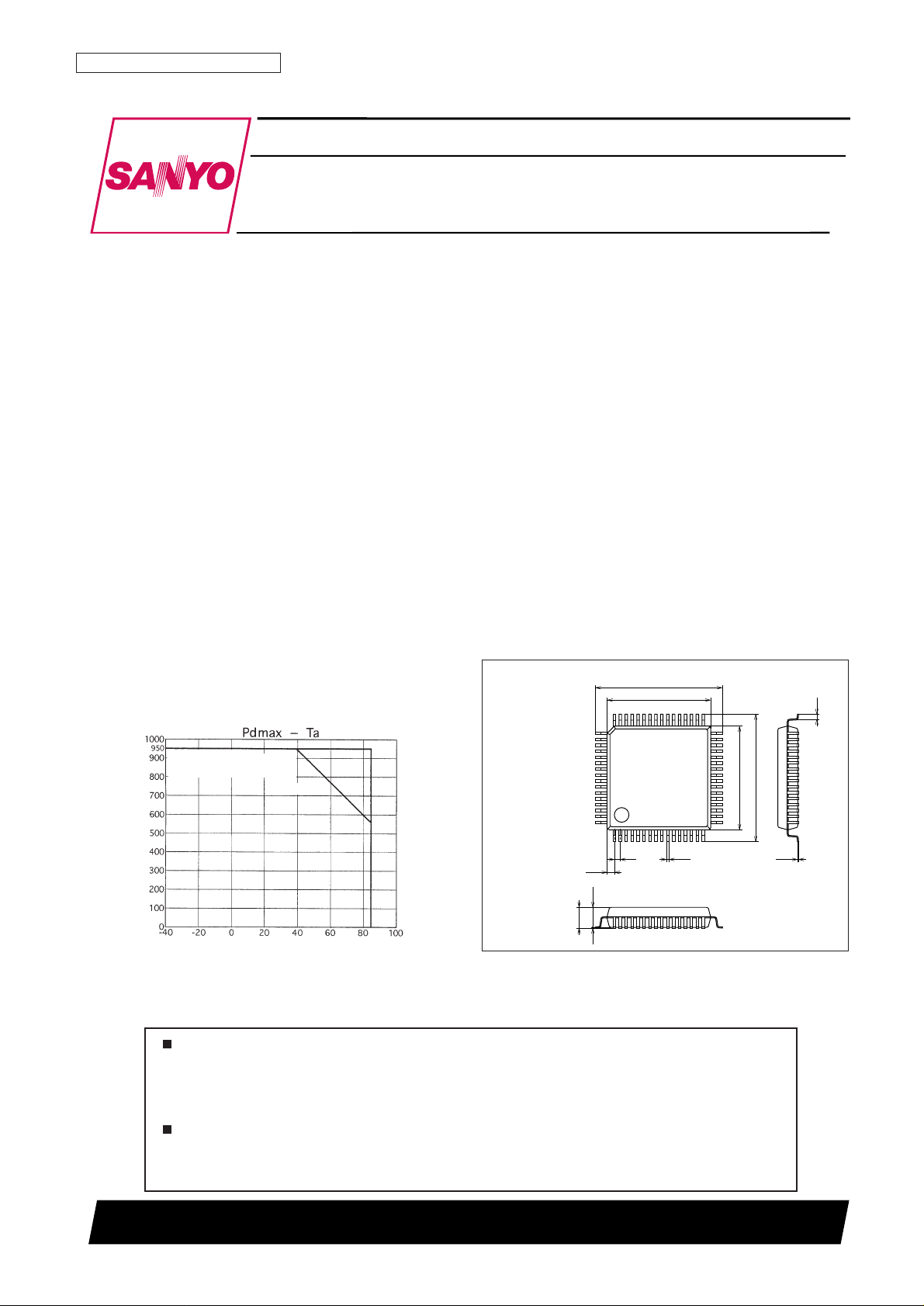
Package Dimensions
Unit:mm
3159A-QIP64E (14 × 14)
Monolithic Linear IC
Ordering number : ENN6655
72602RM (OT) No. 6655-1/54
SANYO Electric Co.,Ltd. Semiconductor Company
TOKYO OFFICE Tokyo Bldg., 1-10, 1 Chome, Ueno, Taito-ku, TOKYO, 110-8534 JAPAN
Single-Chip Tuner IC for Car Radios
LA1787M
14.0
17.2
14.0
17.2
0.15
0.35
0.8
(2.7)
3.0max
0.1
0.8
(1.0)
116
17
32
3348
49
64
Allowable power dissipation,
Pdmax — mW
Ambient temperature, Ta — °C
Mounted on a 40 × 80 × 1.3 mm
3
glass epoxy printed circuit board
Independent IC
SANYO: QIP64E (14 × 14)
[LA1787M]
Ratings
Parameter Symbol Conditions
min typ max
unit
[FM Characteristics] At the FM IF input
Current drain I
CCO
-FM No input, I40 + I45 + I54 + I59 + I60 + I61 60 94 110 mA
Demodulation output V
O
-FM 10.7 MHz, 100dBµ, 1 kHz, 100%mod, The pin 15 output 205 310 415 mVrms
Pin 31 demodulation output V
O
-FM31 10.7 MHz, 100dBµ, 1 kHz, 100%mod, The pin 31 output 190 295 380 mVrms
Channel balance CB The ratio between pins 15 and 16 at 10.7 MHz, 100 dBµ, 1 kHz –1 0 +1 dB
Total harmonic distortion THD-FM mono 10.7 MHz, 100 dBµ, 1 kHz, 100% mod, pin 15 0.3 1 %
Signal-to-noise ratio: IF S/N-FM IF 10.7 MHz, 100 dBµ, 1 kHz, 100% mod, pin 15 75 82 dB
AM suppression ratio: IF AMR IF 10.7 MHz, 100 dBµ, 1 kHz, f
m
= 1 kHz, 30% AM, pin 15 55 68 dB
Att-1
10.7 MHz, 100 dBµ, 1 kHz. The pin 15
5 10 15 dB
attenuation when V33 goes from 0 to 2 V
Muting attenuation Att-2
10.7 MHz, 100 dBµ, 1 kHz. The pin 15
15 20 25 dB
attenuation when V33 goes from 0 to 2 V
*1
Att-3
10.7 MHz, 100 dBµ, 1 kHz. The pin 15
28 33 38 dB
attenuation when V33 goes from 0 to 2 V
*2
Separation Separation
10.7 MHz, 100 dBµ, L+R = 90%, pilot = 10%. The pin 15 output
30 40 dB
ratio
Stereo on level ST-ON The pilot modulation such that V26 < 0.5 V 1.2 2.4 4.4 %
Stereo off level ST-OFF The pilot modulation such that V26 > 3.5 V 0.6 1.6 %
Main total harmonic distortion
THD-Main L 10.7 MHz, 100 dBµ, L+R = 90%, pilot = 10%. The pin 15 signal 0.3 1.2 %
Pilot cancellation PCAN
10.7 MHz, 100 dBµ, pilot = 10%.
20 30 dB
The pin 15 signal/the pilot level leakage. DIN audio
SNC output attenuation AttSNC
10.7 MHz, 100 dBµ, L-R = 90%, pilot = 10%.
1 5 9 dB
V28 = 3 V → 0.6 V, pin 15
AttHCC-1
10.7 MHz, 100 dBµ, 10 kHz, L+R = 90%, pilot = 10%.
0.5 4.5 8.5 dB
HCC output attenuation
V29 = 3 V → 0.6 V, pin 15
AttHCC-2
10.7 MHz, 100 dBµ, 10 kHz, L+R = 90%,
6 10 14 dB
pilot = 10%. V29 = 3 V → 0.1 V, pin 15
Input limiting voltage Vi-lim
100 dBµ, 10.7 MHz, 30% modulation. The IF input such
33 40 47 dBµ
that the input reference output goes down by 3 dB
Muting sensitivity Vi-mute The IF input level (unmodulated) when V33 = 2 V 27 35 43 dBµ
SD-sen1 FM
The IF input level (unmodulated) (over 100 mV rms)
54 62 70 dBµ
SD sensitivity
such that the IF counter buffer output goes on
SD-sen2 FM 54 62 70 dBµ
IF counter buffer output V
IFBUFF-FM
10.7 MHz, 100 dBµ, unmodulated. The pin 23 output 130 200 270 mVrms
V
SM
FM-1 No input. The pin 24 DC output, unmodulated 0.0 0.1 0.3 V
Signal meter output
V
SM
FM-2 50 dBµ. The pin 24 DC output, unmodulated 0.4 1.0 1.5 V
V
SM
FM-3 70 dBµ. The pin 24 DC output, unmodulated 2.0 2.7 3.5 V
V
SM
FM-4 100 dBµ. The pin 24 DC output, unmodulated 4.7 5.5 6.2 V
Muting bandwidth BW-mute 100 dBµ. The bandwidth when V33 = 2 V, unmodulated 150 220 290 kHz
Mute drive output V
MUTE-100
100 dBµ, 0 dBµ. The pin 33 DC output, unmodulated 0.00 0.03 0.20 V
Operating Characteristics at Ta = 25°C, VCC= 8.0V, in the specified test cricuit for the FM IF input
Continued on next page.
No. 6655-2/54
LA1787M
Specifications
Maximum Ratings at Ta = 25°C
Operating Conditions at Ta = 25°C
Parameter Symbol Conditions Ratings Unit
Maximum supply voltage
V
CC
1 max Pins 6, 40, and 61 9 V
V
CC
2 max Pins 7, 45, 54, 59, and 60 12 V
Allowable power dissipation Pd max Ta ≤ 55°C 950 mW
Operating temperature Topr –40 to +85 °C
Storage temperature Tstg –40 to +150 °C
Parameter Symbol Conditions Ratings Unit
Recommended supply voltage
V
CC
Pins 6, 7, 40, 45, 54, 59, 60, and 61 8 V
V
CC
ST IND Pin 26 5 V
Operating supply voltage range V
CC
op 7.5 to 9.0 V
Ratings
Parameter Symbol Conditions
min typ max
unit
[FM FE Mixer Input
N-AGC on input V
N
-AGC
83 MHz, unmodulated.
81 88 95 dBµ
The input such that the pin 2 voltage is 2.0 V or below
W-AGC on input VWAGC
83 MHz, unmodulated. The input such that the pin 2
104 110 116 dBµ
voltage is 2.0 V or below. (When the keyed AGC is set to 4.0 V.)
Conversion gain A.V 83 MHz, 80 dBµ, unmodulated. The FE CF output 19 30 48 mVrms
Oscillator buffer output V
OSCBUFFFM
No input 85 110 165 mVrms
[NC Block] NC input (pin 30)
Gate time τGATE1 f = 1 kHz, for a 1-µs, 100-mV p-o pulse 55 µs
Noise sensitivity SN
The level of a 1 = kHz, 1-µs pulse input that starts
40 mVp-o
noise canceller operation. Measured at pin 30.
The pulse rejection effect provided by the noise canceller.
NC effect SN-NC
For a repeated 1-µs wide pulse, frequency = 10 kHz,
5
150 mV p-o. The ratio of the FM mode pin 15 output
referenced to the AM mode pin 15 output (effective value)
[Multipath Rejection Circuit] MRC input (pin 27)
MRC output VMRC V24 = 5 V 2.2 2.3 2.4 V
MRC operating level MRC-ON
The pin 32 input level at f = 70 kHz such that
10 15 20 mVrms
pin 24 goes to 5 V and pin 27 goes to 2 V
[AM Characteristics] AM ANT input
Practical sensitivity S/N-30 1 MHz, 30 dBµ, f
m
= 1 kHz, 30% modulation, pin 15 20 dB
Detector output V
O
-AM 1 MHz, 74 dBµ, fm= 1 kHz, 30% modulation, pin 15 130 195 270 mVrms
Pin 31 detector output V
O
-AM31 1 MHz, 74 dBµ, fm= 1 kHz, 30% modulation, pin 31 110 175 230 mVms
AGC F.O.M. V
AGC-FOM
1 MHz, 74 dBµ, referenced to the output, the input amplitude
51 56 61 dB
such that the output falls by 10 dB. Pin 15
Signal-to-noise ratio S/N-AM 1 MHz, 74 dBµ, fm= 1 kHz, 30% modulation 47 52 dB
Total harmonic distortion THD-AM 1 MHz, 74 dBµ, f
m
= 1 kHz, 80% modulation 0.3 1 %
Signal meter output
V
SM
AM-1 No input 0.0 0.2 0.5 V
V
SM
AM-2 1 MHz, 130 dBµ, unmodulated 4.8 6 7.3 V
Oscillator buffer output V
OSCBUFF AM1
No input, the pin 15 output 185 230 mVrms
Wide band AGC sensitivity
W-AGCsen1 1.4 MHz, the input when V46 = 0.7 V 92 98 104 dBµ
W-AGCsen2 1.4 MHz, the input when V46 = 0.7 V (seek mode) 83 89 95 dBµ
SD sensitivity
SD-sen1 AM
1 MHz, the ANT input level such that the IF counter output turns on.
24 30 36 dBµ
SD-sen2 AM
1 MHz, the ANT input level such that the SD pin goes to the on state.
24 30 36 dBµ
IF buffer output V
IFBUFF-AM
1 MHz, 74 dBµ, unmodulated. The pin 23 output 200 290 mVrms
No. 6655-3/54
LA1787M
Note: These measurements must be made using the either the IC-51-0644-824 or KS8277 IC socket (manufactured by Yamaichi Electronics).
* 1. When the resistor between pin 58 and ground is 200 kΩ.
* 2. When the resistor between pin 58 and ground is 30 kΩ.
Continued from preceding page.

Function List
FM Front End (Equivalent to the Sanyo LA1193)
• Double input type double balanced mixer
• Pin diode drive AGC output
• MOSFET second gate drive AGC output
• Keyed AGC adjustment pin
• Differential IF amplifier
• Wide band AGC sensitivity setting pin, and narrow
band AGC sensitivity setting pin
• Local oscillator
FM IF
• IF limiter amplifier
• S-meter output (also used for AM) 6-stage pickup
• Multipath detection pin (shared FM signal meter)
• Quadrature detection
• AF preamplifier
• AGC output
• Band muting
• Weak input muting
• Soft muting adjustment pin
• Muting attenuation adjustment pin
• IF counter buffer output (also used for AM)
• SD (IF counter buffer on level) adjustment pin
• SD output (active high) (also used for AM)
Noise Canceller
• High-pass filter (first order)
• Delay circuit based low-pass filter (fourth order)
• Noise AGC
• Pilot signal compensation circuit
• Noise sensitivity setting pin
• Function for disabling the noise canceller in AM
mode
Multiplex Functions
• Adjustment-free VCO circuit
• Level follower type pilot canceller circuit
• HCC (high cut control)
• Automatic stereo/mono switching
• VCO oscillation stop function (AM mode)
• Forced monaural
• SNC (stereo noise controller)
• Stereo display pin
• Anti-birdie filter
AM
• Double balanced mixer (1st, 2nd)
• IF amplifier
• Detection
• RF AGC (narrow/wide)
• Pin diode drive pin
• IF AGC
• Signal meter output (also used for FM)
• Local oscillator circuits (first and second)
• Local oscillator buffer output
• IF counter buffer output (also used by the FM IF)
• SD (IF counter buffer on level) adjustment pin
• SD output (active high) (also used for AM)
• Wide AGC
• Detection output frequency characteristics
adjustment pin (low cut, high deemphasis)
• AM stereo buffer
MRC (multipath noise rejection circuit)
AM/FM switching output (linked to the FM VCC)
No. 6655-4/54
LA1787M
Operating Characteristics and Symbols Used in the Test Circuit Diagrams
Switches (SW)
Switch on = 1, SW off = 0
There are two switches that use signal transfer.
— SW2: switches between the mixer input and the IF input.
— SW4: switches between noise canceler input and IF output + noise canceler input.
No. 6655-5/54
LA1787M
Types of SG used
PG1 (AC1) Used for noise canceler testing. A pulse generator and an AF oscillator are required.
AC2 Used for FM front end testing. Outputs an 83 MHz signal.
AC3 Used for FM IF, noise canceler, and MPX testing. Outputs a 10.7 MHz signal. Stereo modulation must be possible.
AC4 Used for AM testing. Outputs 1 MHz and 1.4 MHz signals.
AC5 Used with the MRC. Can also be used for AF and OSC.
Power supply
V
CC
8 V
V
CC
1 5 V SD, stereo, seek/stop
V
CC
2 0.1 V / 0.7 V / 2 V / 4 V
These levels
Keyed AGC, Mute ATT
V
CC
3 0.1 V / 0.6 V / 2 V
must be variable.
HCC, SNC, SASC (MRC)
• Trimmers (variable resistors)
VR1 Separation adjustment
VR2 Pilot cancellation adjustment
• AC voltages
VA1 AM/FM OSC Buff Pin 4
VA2 First IF output Pin 53 → CF → pin 51 load level (10.7 MHz)
VA3 IF counter buffer Pin 23 (10.7 MHz/450 kHz)
VA4 MPX OUT Left ch Pin 15 (AF)
VA5 MPX OUT Right ch Pin 16 (AF)
Test Points
• DC voltages
VD1 FM RF AGC voltage Pin 2
VD2 AM/FM SD, AM Tweet, FM stereo indicator Pin 26
VD3 AM/FM S-meter Pin 24
VD4 MRC output Pin 27
VD5 Mute drive output Pin 33
VD6 AM antenna damping voltage Pin 46
VD7 N.C. Gate time Pin 8
• Switches
Parameter ON OFF
SW1 AM/FM switching. The FE V
CC
is supplied to pin 62. FM AM
SW2 FM IF switching. Pin 51/FE output FE IF OUT (A) AC3 (B)
SW3 For conversion gain testing Conversion gain measurement (A) Other/purposes
SW4
For switching between noise canceler input and IF output + noise canceler.
AC1 (A) Other/purposes
SW5 High-speed SD High-speed SD Other/purposes
SW6 SEEK/STOP (IF BUFF ON/OFF) STOP Seek (IF buffer output)
SW7 MUTE ATT 200 kΩ MUTE 200 kΩ OFF
SW8 MUTE ATT 30 kΩ MUTE 30 kΩ OFF
SW9 For pilot cancellation testing When pilot cancellation is used When pilot cancellation is not used
SW10 Mute off (pin 33) MUTE OFF MUTE ON
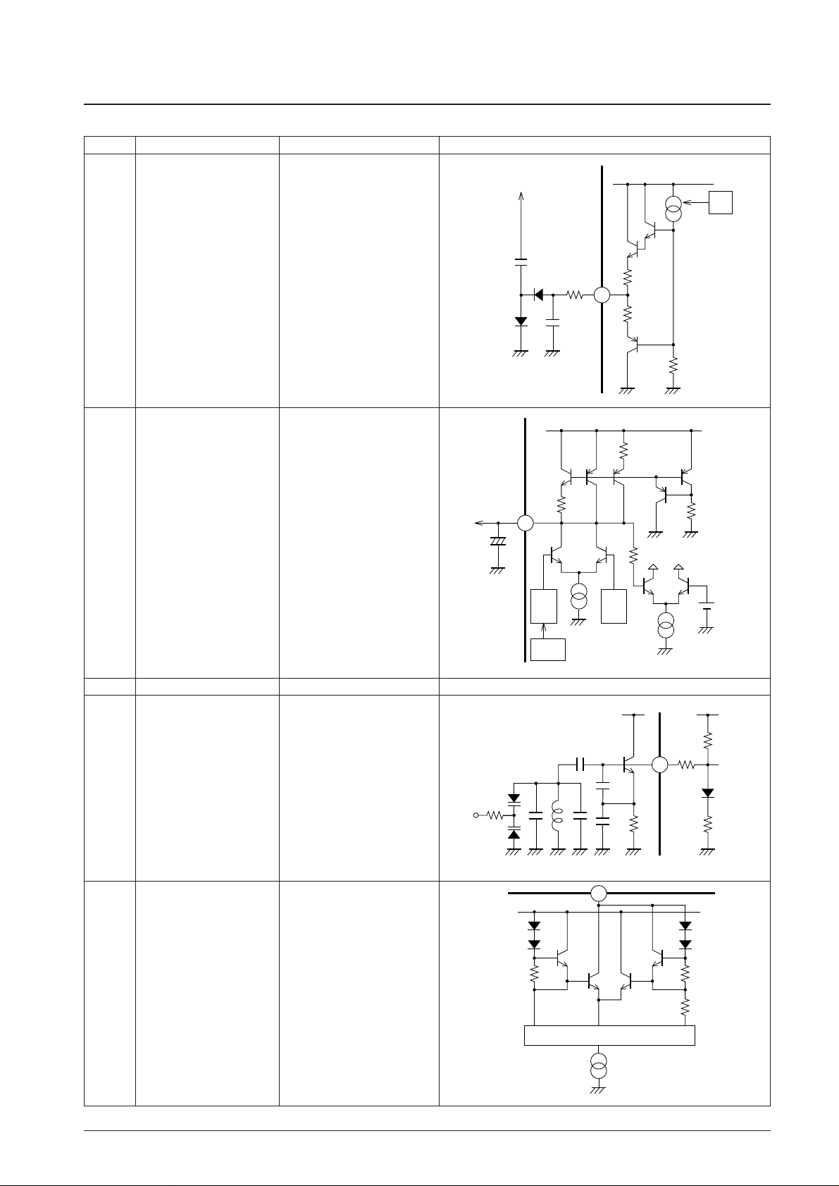
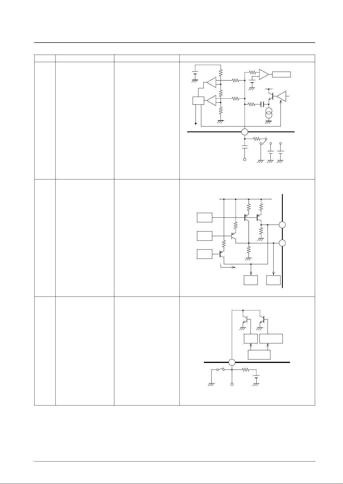
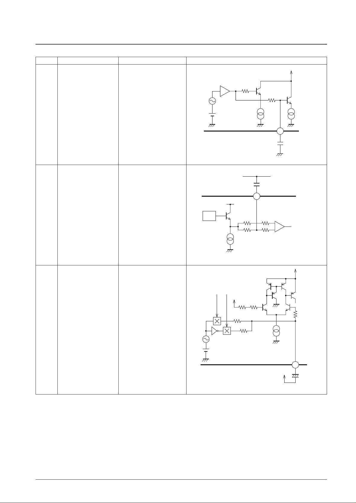
Pin No. Function Description Equivalent circuit
3 F.E.GND
Pin Descriptions
No. 6655-6/54
LA1787M
1
ANT
1000pF
1000pF
100Ω
100Ω
300Ω
V
CC
62 pin
RF
AGC
A13555
+
2
N
AGC
DET
W
AGC
DET
KEYED
AGC
ANT
DAMPING
DRIVER
V
CC
V
CC
12kΩ
FET
2nd GATE
A13556
4
V
CC
25pF
20pF
2kΩ
V
T
A13557
An antenna damping current flows
1 Antenna damping drive when the RF AGC voltage (pin 2)
reaches V
CC
– VD.
2 RF AGC
Used to control the FET
second gate.
4 OSC Oscillator connection
AM first oscillator
7 AM OSC
This circuit can oscillator up to the
SW band.
An ALC circuit is included.
Continued on next page.
7
A L C
V
CC
A13558
No. 6655-7/54
LA1787M
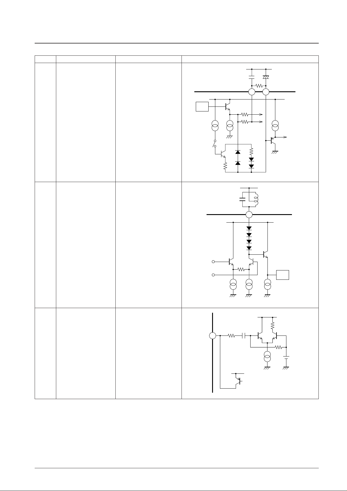
Pin No. Function Description Equivalent circuit
13 Pilot input Pin 13 is the PLL circuit input pin.
14 N.C, MPX, MRC, GND
Ground for the N.C., MPX, and
MRC circuits.
After setting up the medium field
(about 50 dBµ) sensitivity with the
8 Noise AGC sensitivity noise sensitivity setting pin (pin 8),
9 AGC adjustment set the weak field (about 20 to
30 dBµ) sensitivity with the AGC
adjustment pin (pin 9)
11
Memory circuit connection
Recording circuit used during
12 noise canceller operation.
Continued from preceding page.
Continued on next page.
3kΩ
3kΩ
15kΩ
200Ω
8 9
3kΩ
V
CC
1MΩ
Differential
amp
0.01µF
0.01µF 6800pF
13 12 11
3.9kΩ
+
0.47µF
A13559
circuit
Gate
LPF
N.C
12 13
0.01µF
30kΩ
A13560
V
CC
PLL
A13561
No. 6655-8/54
LA1787M
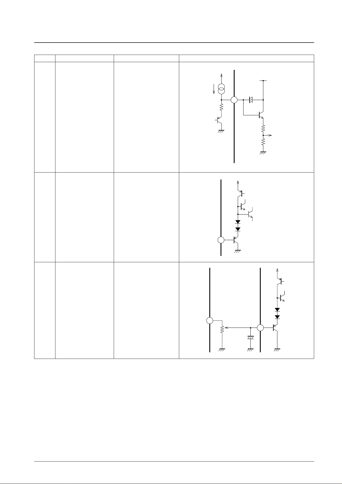
Pin No. Function Description Equivalent circuit
15 MPX output (left)
Deemphasis
16 MPX output (right)
50 µs: 0.015 µF
75 µs: 0.022 µF
Adjustment is required since the
pilot signal level varies with the
17 Pilot canceller signal output sample-to-sample variations in
the IF output level and other
parameters.
18 Pilot canceller signal output
Pin 18 is the output pin for the
pilot canceller signal.
Continued from preceding page.
Continued on next page.
V
CC
3.3kΩ
3.3kΩ
15
0.015µF 0.015µF
V
20kΩ
10kΩ
17 18
0.01µF
CC
V
16
100kΩ
CC
A13562
6.7kΩ
A13563
17 18
0.01µF
100kΩ
1.5kΩ
A13564
No. 6655-9/54
LA1787M
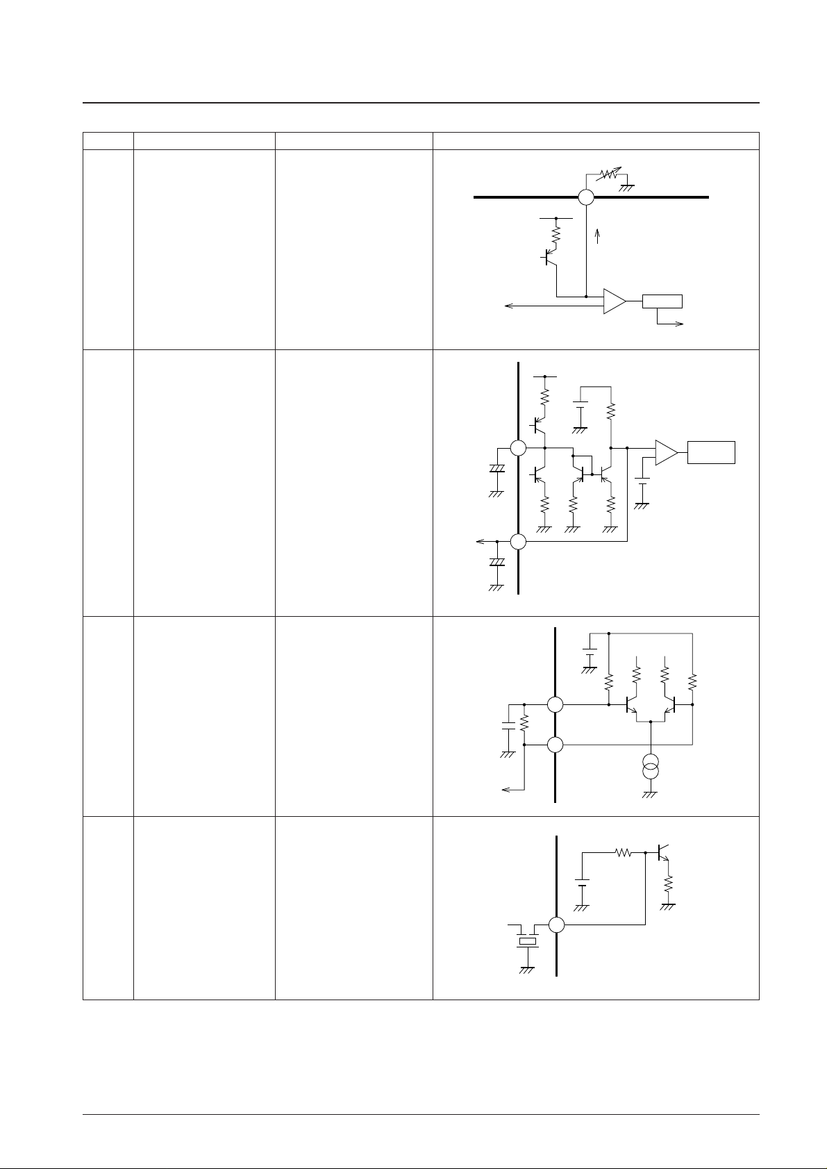
Pin No. Function Description Equivalent circuit
20 VCO The oscillator frequency is 912 Hz.
KBR-912F108
(Kyocera Corporation)
CSB-912JF108
(Murata Mfg. Co., Ltd.)
Use a trimmer to adjust the
19
Separation subdecoder input level.
adjustment pin (The output level is not modified in
mono and main modes.)
21 PHASE COMP.
22 PHASE COMP.
Continued from preceding page.
Continued on next page.
Composite
signal
V
4kΩ
REF
5kΩ
19
CSB
912
JF108
10pF
DECODER
30kΩ
0.047µF
A13565
20
A13566
V
REF
15kΩ
+
19kΩ
15kΩ
21 22
+
+
A13567
No. 6655-10/54
LA1787M
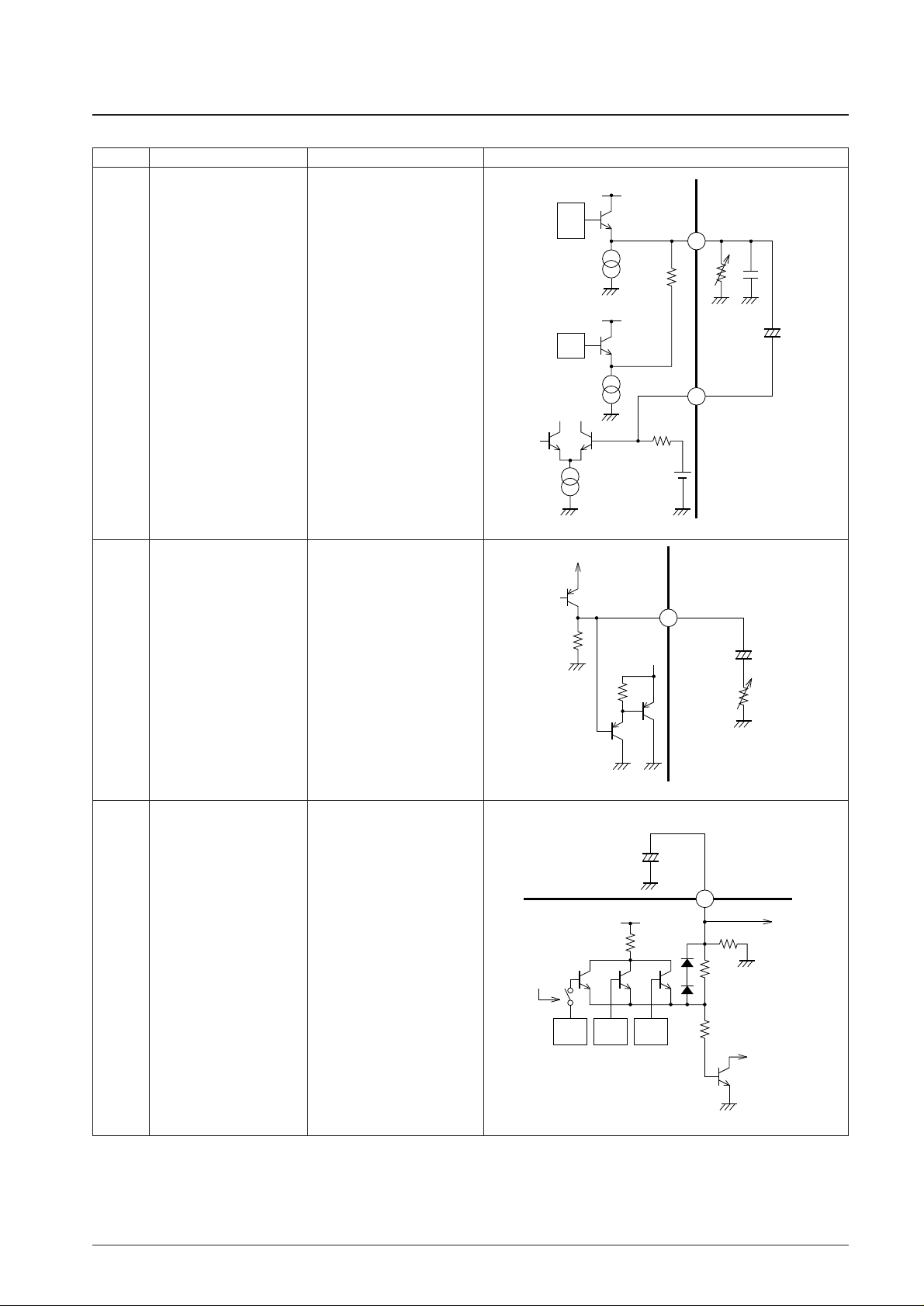
Pin No. Function Description Equivalent circuit
Continued from preceding page.
Continued on next page.
This pin functions both as the IF
counter buffer (AC output) and as
the seek/stop switch pin.
The voltage V23 switches
between the following three
modes.
23
IF counter buffer seek/stop During FM reception:
switching 5 V: Seek mode
2.5 V: Forced SD mode
0 V: Reception mode
AM reception
(two modes: 0 and 5 V)
5 V: Seek mode
0 V: Reception mode
24 AM/FM signal meter Fixed-current drive signal meter
output
In AM mode, pin 32 outputs a
32 Dedicated FM signal meter 1-mA current. Thus the HCC
circuit is turned off.
The voltage V23 switches
between three modes as follows.
FM reception:
5 V: The SD pin operates linked
to the IF counter buffer.
26 Stereo indicator for the SD pin
2.5 V: Forced SD mode: operates
as the SD pin.
0.7 V: Reception mode: stereo
indicator
AM reception: (two modes: 0 and 5 V)
5 V: Operates as the seek SD pin.
0 V: Reception mode. Not used.
SD
4.9V
SW
S-meter
S-meter
AM/FM
FM
AM
SW
+
1.3V
50F
–
V
CC
Forced
SD: 2.5V
AM MUTE
IF counter
buffer
SEEK
5V
32
24
A13568
+
–
+
–
50kΩ
10kΩ
150Ω
23
51kΩ
STOP
IF
BUFF.
V
CC
10kΩ
10kΩ
Outputs a 1-mA
current during AM
reception
26
MRC
AM/FMSDStereo
Seek/stop
switching
100kΩ
V
AM/FM
SW
indicator
DD
A13570
A13569
No. 6655-11/54
LA1787M
Pin No. Function Description Equivalent circuit
Continued from preceding page.
Continued on next page.
The MRC detector time constant
27 MRC control voltage time
is determined by a 100 Ω resistor
constant
and C2 when discharging and by
the 2-µA current and C2 when
charging.
28 SNC control input
The sub-output is controlled by a
0 to 1-V input.
The high band frequency output is
controlled by a 0 to 1-V input.
It can also be controlled by the
29 HCC control input MRC output.
Use a resistor of at least 100 kΩ
when controlling with the pin 32
FM S-meter signal.
V
CC
2µA
C2
27
V
REF
100Ω
V
CC
+
Pin 28
A13571
28
A13572
V
REF
32
29
+
1µF
A13573
No. 6655-12/54
LA1787M
Pin No. Function Description Equivalent circuit
Continued from preceding page.
Continued on next page.
30 Noise canceller input
Pin 30 is the noise canceller input.
The input impedance is 50 kΩ.
Pin 31 is the AM and FM detector
output
In FM mode, this is a lowimpedance output.
31 AM/FM detector output In AM mode, the output
impedance is 10 kΩ.
To improve the low band
separation, use a coupling
capacitor of over 10 µF.
FM S-meter output block
32 IF S-meter output and MRC
MRC AC input block
DC input
Adjust the external 1-kΩ resistor
to attenuate the MRC AC input
and control the circuit.
•The muting time constant is
determined by an external RC
circuit as described below.
Attack time: T
A
= 10 kΩ × C1
Release time: T
R
= 50 kΩ × C1
•Noise convergence adjustment
33 Mute drive output The noise convergence can be
adjusted when there is no input
signal by inserting a resistor
between pin 33 and ground.
•Muting off function
Ground pin 33 through a 4-kΩ
resistor.
V
CC
FM
detector
output
31
detector
10kΩ
AM
10kΩ
V
CC
1µF
+
30
Noise
canceller
50kΩ
4.2V
A13574
V
CC
32
+
1µF
1kΩ
MRC input
SEEK
OFF
SOFT
MUTE
HOLE
DET
V
CC
+
Band
muting
C1
0.1µF
A13575
33
50kΩ
10kΩ
50kΩ
MUTE
AMP.
SD circuit
A13576
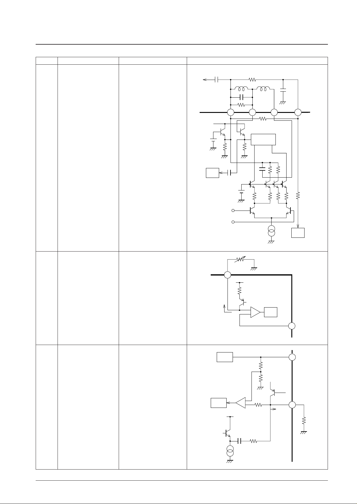
No. 6655-13/54
LA1787M
Pin No. Function Description Equivalent circuit
Continued from preceding page.
Continued on next page.
•The resistor R
1
determines the
width of the band muting function.
Increasing the value of R
1
narrows the band.
Reducing the value of R
1
widens
the band.
34 AGC
35 QD output
•Null voltage
36 QD input
When tuned, the voltage between
37 V
REF
pins 34 and 37, V
34 – 37
, will be 0 V.
The band muting function turns
on when |V
34 – 37
| ≥ 0.7 V.
V
37
= 4.9 V
A 130-µA current flows from pin
38 FM SD ADJ
38 and, in conjunction with the
external resistance R, determines
the comparison voltage.
The keyed AGC operates when
the voltage created by dividing the
pin 24 S-meter output voltage by
the 6.4 and 3.6 kΩ resistors
39 Keyed AGC becomes lower than the voltage
AM stereo buffer determined by the resistor
between pin 39 and ground.
This pin also is used as the AM
stereo IF buffer pin.
0.1µF
V
REF
V
CC
37 36 35 34
V
CC
HOLE
DET
IF limitter amplifier
R1
C
R2
Quadrature
detector
3pF
R
SD ADJ
390Ω
1kΩ
Band
muting
A13577
130µA
KEYED
AGC
AM IF out
38
S-meter
Comparator
Comparator
+
–
1.3V
V
CC
50pF
150Ω
+
SD
–
24
S-meter
A13578
24
6.4kΩ
3.6kΩ
39
90µA
A13579
No. 6655-14/54
LA1787M
Pin No. Function Description Equivalent circuit
Continued from preceding page.
Continued on next page.
The HCC frequency characteristics
41 HCC capacitor
are determined by the external
capacitor connected at this pin.
This pin is used to change the
frequency characteristics of the
unneeded audio band under
100 Hz in AM mode to produce
a clear audio signal.
Note: The LC capacitor must be
connected between this pin
and V
CC
(pin 40).
42 AM L.C. pin This is because the detector
circuit operates referenced
to V
CC
.
The cutoff frequency f
C
is
determined by the following
formula.
f
C
= 1/2π × 50 kΩ × C
Inserting a 1-MΩ resistor between
43 Pilot detector pin 43 and V
CC
will force the IC
to mono mode.
20kΩ
+
20kΩ
V
CC
DET
41
2200pF
A13580
V
CC
C
50kΩ
50kΩ
42
1kΩ
+
–
1kΩ
A13581
V
CC
V
CC
+
19kHz∠0°
BIAS
30kΩ
30kΩ
30kΩ
43
1µF
+
A13582
No. 6655-15/54
LA1787M
Pin No. Function Description Equivalent circuit
45 IF output The IF amplifier load
Continued from preceding page.
Continued on next page.
G1; Used for time constant
switching during seeks.
• Reception
τ = 2.2 µF × 300 kΩ
44 IF AGC
• Seek
τ = 2.2 µF × 10 Ω
The external capacitors are
connected to V
CC
.
This is because the IF amplifier
operates referenced to V
CC
.
AM antenna damping I46 = 6 mA (maximum)
46 drive output This is the antenna damping
Wide band AGC input current.
DET
SEEK
ON
0.022µF
G1
10Ω
240kΩ
42
50kΩ
50kΩ
+
44
Pin 40 V
V
C
2.2µF
CC
CC
V
CC
IF
AGC
A13583
45
Pin 40 V
CC
DET
A13584
V
CC
50pF
46
V
100Ω
CC
ANT DAMPING
DRIVER
20kΩ
W.AGC AMP.
A13585
No. 6655-16/54
LA1787M
Pin No. Function Description Equivalent circuit
52 IF input The input impedance is 2 kΩ.
Continued from preceding page.
Continued on next page.
FM muting on level
Modify the value of the external
47
adjustment
resistor to adjust the muting on
level.
RF AGC rectification capacitor
The low frequency distortion is
determined as follows:
Increasing C48 and C57 improves
48 RF AGC bypass the distortion but makes the
57 RF AGC response slower.
Reducing C48 and C57
aggravates the distortion but
makes the response faster.
50 IF bypass
51 FM IF input
Due to the high gain of the limiter
amplifer, care must be taken when
choosing the grounding point for
the limiter amplifer input capacitor
to prevent oscillation.
30kΩ
47
140µA
Pin 24
V
CC
V
CC
R
–
+
Inverter
MUTE
A13586
+
3.3µF
For AGC use
+
47µF
0.022µF
IF in
5.6V
48
57
2.6V
50
330Ω
51
10kΩ
10kΩ
Antenna
+
damping
–
A13587
10kΩ
A13588
2kΩ
100Ω
52
A13589
No. 6655-17/54
LA1787M
Pin No. Function Description Equivalent circuit
Continued from preceding page.
Continued on next page.
• Input and output pin or the first
IF amplifier
• Inverting amplifier
53 IF amplifier output V56 = 2 V
56 IF amplifier input Input impedance: R
IN
= 330 Ω
V53 = 5.3 V
Output impedance
R
OUT
= 330 Ω
The mixer coil connected to the
54 Mixer output: 130 µA
pin 54 mixer output must be
49 Mixer input
wired to V
CC
(pin 40).
The pin 49 mixer input
impedance is 330 Ω
Pins 55 and 58 include built-in
DC cut capacitors.
The AGC on level is determined
by the values of the capacitors
C1 and C2.
55 W-AGC IN Pin 55 functions as the SD
AM SD ADJ sensitivity adjustment pin in
AM mode.
58 N-AGC IN
Muting attenuation The output current I55 is 50 µA,
adjustment pin and V55 varies depending on the
value of the external resistor.
The SD function operates by
comparing V55 with the S-meter
voltage.
53
IF OUT
IF IN
Pin 40 V
300Ω
2.75V
56
CC
Pin 40 VCC
54
V
CC
300Ω
A13590
MIX
IN
MIX
OUT
C1
C2
OSC
49
330Ω
A13591
62 pin
V
CC
30pF
55
58
W-AGC N-AGC
50pF
50µA
+
–
AM SD
Signal meter
A13592
 Loading...