


LA4598
Ordering number: EN4087C
Monolithic Linear IC
LA4598
Two-channel Power Amplifier for Radio Cassette
Players (No Heat Sink Needed during 9 V Operation)
Overview
The LA4598 is a two-channel power IC that is intended for
use in portable audio equipment. Needing no heat sink during
9 V operation facilitates set design with a small footprint.
Functions
.
Thermal shutdown protector built in.
.
Standby switch built in.
Features
.
No heat sink needed during 9 V operation
.
PO= 2.9 W × 2(VCC=9V,RL= 3.2 Ω, THD = 10%).
.
Less quiescent current. (VCC= 9 V, 20 mA, typ).
.
Operating voltage range: VCCop = 4.2 to 16 V.
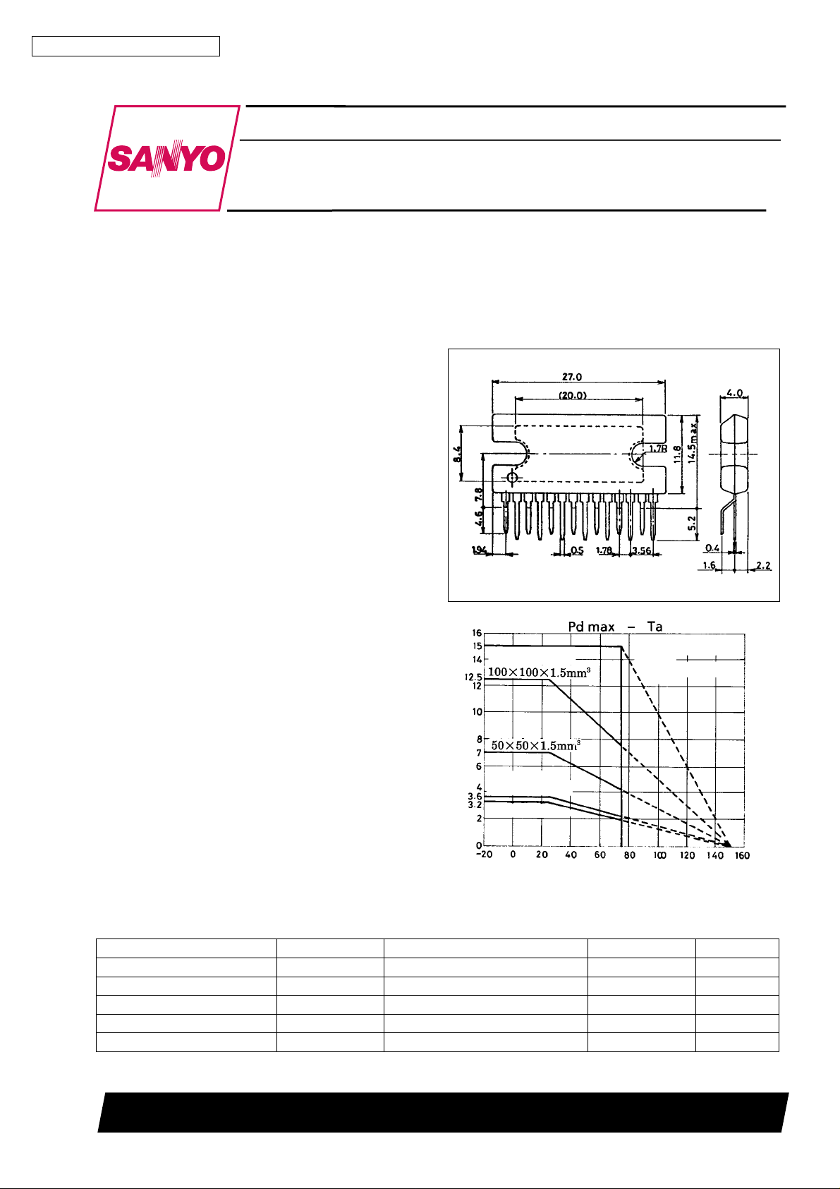
Package Dimensions
unit : mm
3113-SIP14HZ
[LA4598]
Al heat sink tightening
With arbitrarily large heat
sink
torque 4kg.cm
SANYO : SIP14HZ
With silicone grease
applied
With Sanyorecommended board
Independent IC
Allowable power dissipation, Pd max − W
Specifications
Ambient temperature, Ta −°C
Maximum Ratings atTa=25°C
Parameter Symbol Conditions Ratings Unit
Maximum supply voltage V
Allowable power dissipation Pd max* No heat sink 3.6 W
Junction temperature Tj max +150
Operating temperature Topr –20 to +75
Storage temperature Tstg –40 to +150
* With Sanyo-recommended board (9.0 cm × 8.5 cm × 1.5 mm (thickness))
max 18 V
CC
SANYO Electric Co.,Ltd. Semiconductor Bussiness Headquarters
TOKYO OFFICE Tokyo Bldg., 1-10, 1 Chome, Ueno, Taito-ku, TOKYO, 110 JAPAN
D3095HA/N1792TS(II) No.4087-1/9
C
°
C
°
C
°
LA4598
Operating Conditions atTa=25°C
Parameter Symbol Conditions Ratings Unit
Recommended supply voltage V
Recommended load resistance R
Operating voltage range V
CC
L
op 4.2 to 16.0 V
CC
Operating Characteristics atTa=25°C, VCC=9V,f=1kHz, Rg = 600 Ω,RL= 3.2 Ω
Parameter Symbol Conditions min typ max unit
Quiescent current I
Voltage gain VG 47 49 51 dB
Output power
Total harmonic distortion THD V
Input resistance ri 20 30 kΩ
Output noise voltage
Ripple rejection ratio Rr Rg = 0, fr = 100 Hz, V
Channel separation CH Sep Rg = 10 kΩ,V
Standby current Isd 10 µA
CCO
P
1 THD = 10% 2.2 2.9 W
O
P
2 THD = 10%, RL=4Ω 2.3 W
V
V
O
NO1
NO2
= 2 V 0.3 1.0 %
O
Rg = 0, B.P.F = 20 Hz to 20 kHz 0.4 1.0 mV
Rg=10kΩ, B.P.F = 20 Hz to 20 kHz 0.6 2.0 mV
r = 150 mV 40 50 dB
CC
=0dB 45 55 dB
O
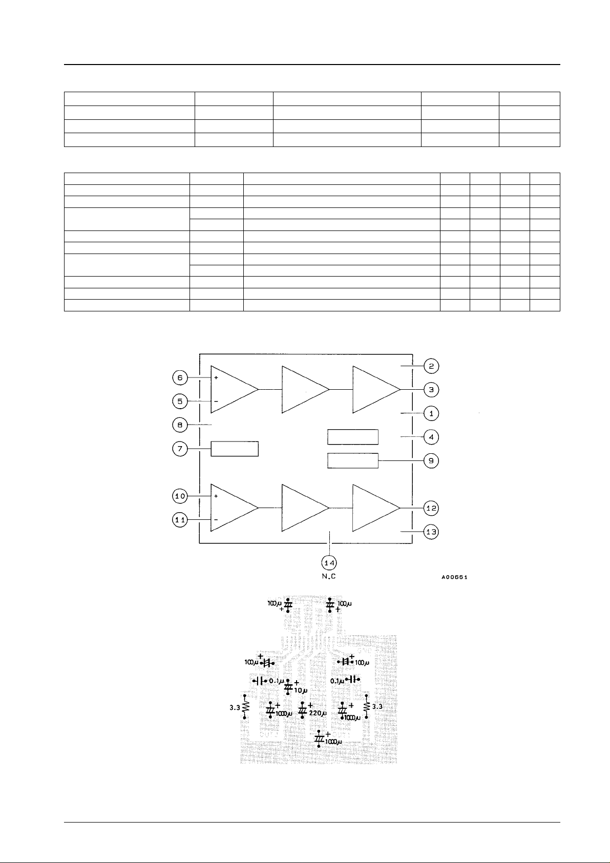
Block Diagram
9V
3.2 Ω
10 20 40 mA
ch1 Input
ch1 NF
Pre GND
D.C
ch2 Input
ch2 NF
Sample Print Pattern
Input
amplifier
Bias circuit
Input
amplifier
Predrive
amplifier
Predrive
amplifier
Power
amplifier
Thermal shutdown
protector
Standby switch
Power
amplifier
ch1 BS
ch1 output
Power GND
V
CC
Standby
ch2 output
ch2 BS
Copper-foiled side 85 × 90 mm
2
Unit (resistance: Ω, capacitance: F)
No.4087-2/9
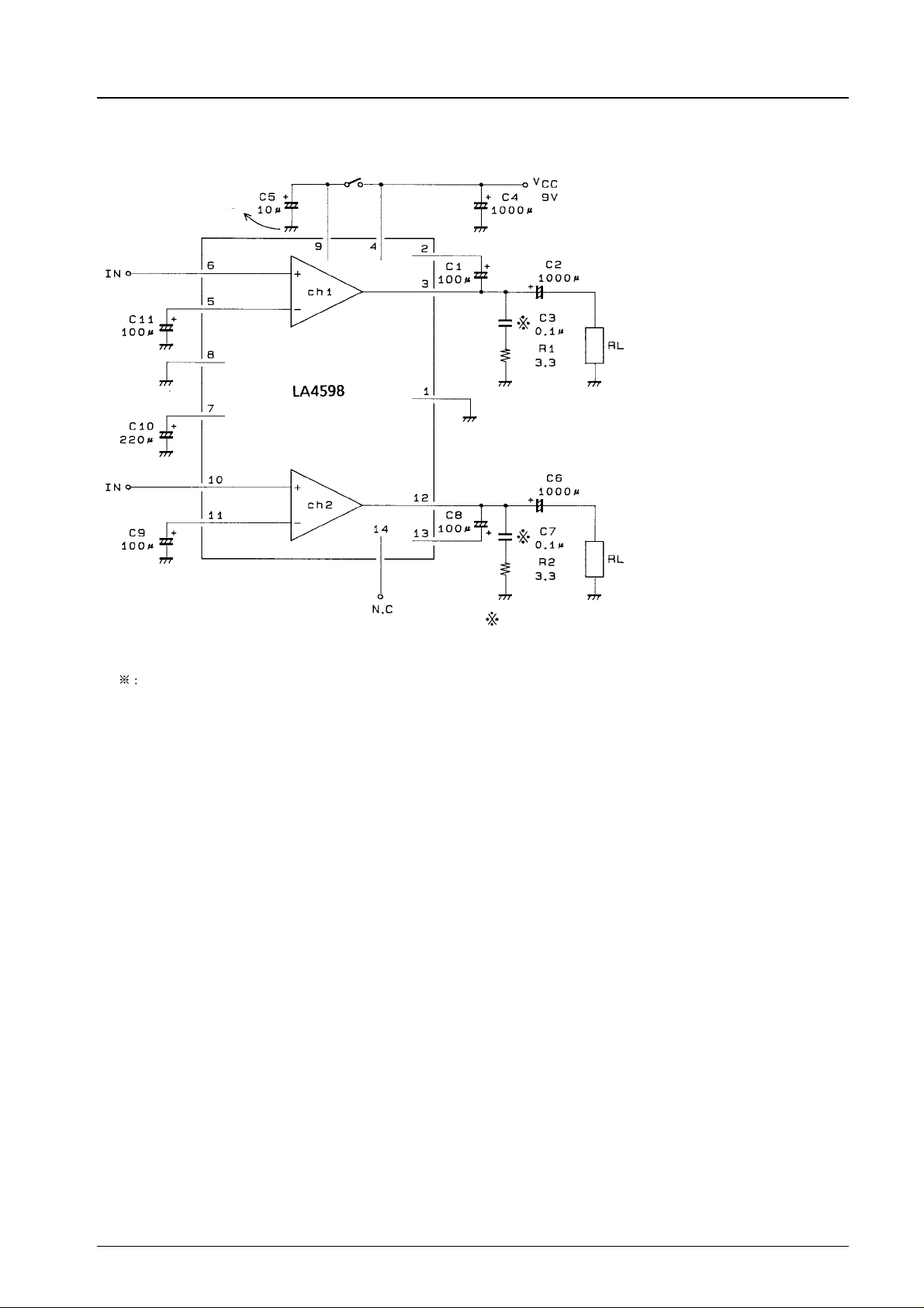
Sample Application Circuit
To large signal GND
LA4598
Mylar capacitor
Unit (resistance:Ω, capacitance:F)
Mylar capacitor
C + R can be added to the negative side of the output capacitor.
However, this is true only for a Sanyo-recommended board; for a set board, artwork must also be
considered.
Description of External Components
C1,C8: Bootstrap capacitors
These capacitors affect low-region output; if the capacitor value is reduced, the low-region output decreases. Therefore,
47 µF or more is desirable.
C
: Output capacitors
2,C6
If the capacitor value is reduced, low-region roll-off frequency f
C
: Oscillation blocking capacitors
3,C7
Mylar capacitor, which is excellent in temperature characteristics and frequency characteristics is used.
C
: Power supply capacitor
4
The capacitor values depends on the power supply line loads (motor, and the like.) and transformer ripple component.
1000 µF to 2200 µF is recommended.
C
: Standby capacitor
5
Pop noise reduction capacitor
C
: Feedback capacitors
9,C11
In addition to affecting low-region roll-off frequency f
C
: Decoupling capacitor
10
, if the capacitor value is increased, the start-up time is extended.
L
This capacitor absorbs power supply ripples; 220 µF is recommended.
and low-region Po worsen.
L
R
: Oscillation blocking resistors
1,R2
The resistor value may be varied 3.3 Ω to 1.0 Ω.
No.4087-3/9
 Loading...