


Ordering number: EN 3507
Monolithic Linear IC
LA1136N, 1136NM, 1137N, 1137NM
AM Tuners for Car Radios and Home Stereos
Overview
The LA1136N/NM and LA1137N/NM are high-performance AM electronic tuner ICs offering sophisticated functions. They are especially suited for use in car radio and home stereo (antenna: loop) applications.
Functions
. MIX
. OSC (with ALC)
. IF amplifier
. Detector
. AGC (normal)
. RF wide-band AGC
. Auto search stop signal (Signal meter output)
. Local oscillation buffer output
. IF band switching circuit (for LA1136N only)
. IF count buffer
. Stop detector output (can be set independently)
. Tweet prevention circuit
. AGC (RF, IF) time constant switching circuit
. IF AGC circuit
. Pin-diode driver
. AM stereo decoder IF output (for LA1136N only)
. Circuit preventing incorrect seek operation
Features
. Excellent cross modulation characteristic: Meets the requirements for preventing not only adjacent-channel interference but also interference caused by all channels
. within broadcast band.
Narrow-band signal meter output: Usable as auto search stop
. signal. Has linearity up to 100 dBµ.
Local oscillation buffer output: Facilitates designing of
. electronic tuner system, frequency display, etc. OSC (with ALC): Improves tracking error because
oscillation output is stabilized at a low level (350 mVrms:
. LA1137N) for varactor diode.
MIX: Double-balanced differential MIX meeting the requirements for preventing spurious interference, IF
. interference.
Good characteristic at high input: 130 dBµ input
. fm = 400 Hz 80%mod THD = 0.5% typ.
. High S/N: Good S/N at medium input (55 dB typ). Usable sensitivity: (S/N = 20 dB input): 25 dBµ
. (when using 2SK715 )
VCC variation compensation: Less variation in gain, distortion: 8 to 12 V
AM stereo capability (LA1136N only)
. IF band switching circuit on chip; controlled by
. microcontroller
Oscillating circuit for AM stereo; SUB S/N improved to
. 6 dB
. IF output for AM stereo decoder
Improved tweet characteristics: 10 dB increase, controlled by
. microcontroller
Improved cross modulation characteristics, especially sensitivity suppression characteristics: 15 dB improvement,
. wide-band AGC operation even for SW band interference
. Improved low-frequency modulation distortion
. Improved temperature characteristics: S-meter, SD sensitivity Faster RF AGC response: RF: 1/3; IF: 1/8 (compared to
. predecessors)
Improved capability for driving external RF AGC transistors:
. IB max = 200 µA
Measures. to prevent incorrect seek operation
.IF count buffer on chip; controlled by microcontroller Time constant switching circuit on chip for RF and IF
.AGC
.IF AGC clear circuit on chip
Measures that prevent stopping one station too soon
SANYO Electric Co.,Ltd. Semiconductor Bussiness Headquarters
TOKYO OFFICE Tokyo Bldg., 1-10, 1 Chome, Ueno, Taito-ku, TOKYO, 110 JAPAN
93097HA(II)/4281TS(US) No.3507-1/28
LA1136N, 1136NM, 1137N, 1137NM
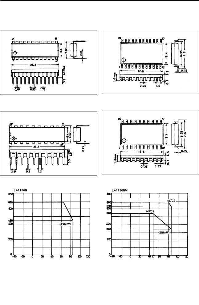
Package Dimensions
unit : mm
3067-DIP24S
[LA1136N]
SANYO : DIP24S
unit : mm
3021B-DIP20S
[LA1137N]
SANYO : DIP20Slim
Pd max ± Ta
Allowable power dissipation, Pd max ± mW
Ambient temperature, Ta ± °C
unit : mm
3112-MFP24S
[LA1136NM]
SANYO : MFP24S
unit : mm
3036B-MFP20
[LA1137NM]
SANYO : MFP20
|
|
Pd max ± Ta |
|
mW |
Mounted on 20 |
× 40 × 1.5 mm PCB |
|
max ± |
|||
Independent IC |
|
||
Allowable power dissipation, Pd |
|
||
|
|
Ambient temperature, Ta ± °C
No. 3507-2/28
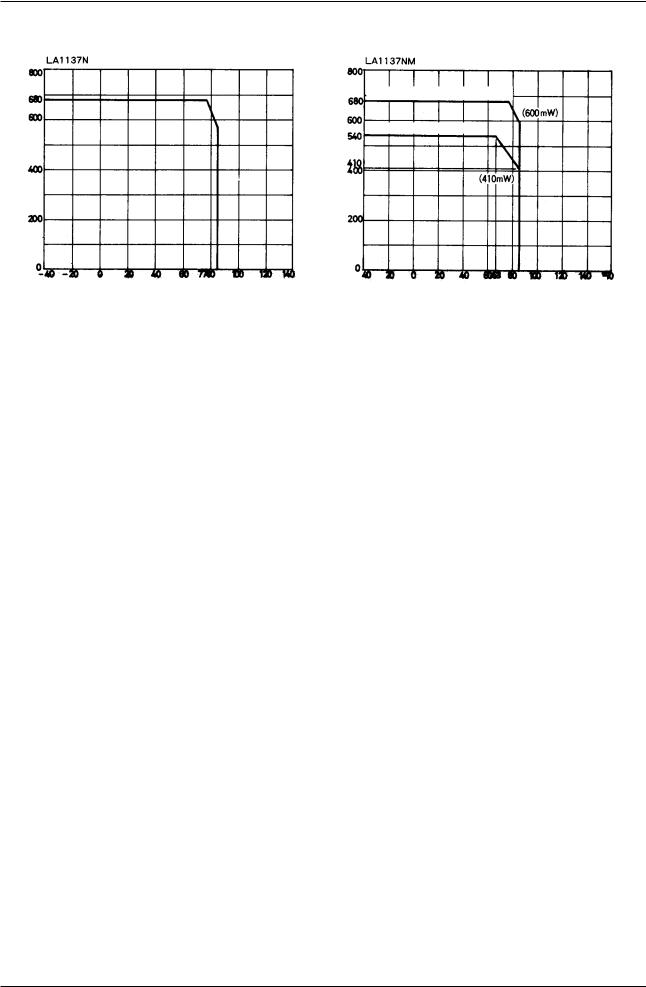
LA1136N, 1136NM, 1137N, 1137NM
|
Pd max ± Ta |
Allowable power dissipation, Pd max ± mW |
Allowable power dissipation, Pd max ± mW |
Ambient temperature, Ta ± °C
Pd max ± Ta
Mounted on 20 × 40 × 1.5 mm PCB
Independent IC
Ambient temperature, Ta ± °C
Specifications
Maximum Ratings at Ta = 25°C
Parameter |
Symbol |
Conditions |
Ratings |
Unit |
|
|
|
|
|
Maximum supply voltage |
VCC max |
Pin 19 (LA1136N), Pin 15 (LA1137N) |
12 |
V |
Output voltage |
VO1 |
Pin 6 |
13.4 |
V |
|
VO2 |
Pin 13 (LA1136N), Pin 10 (LA1137N) |
15.5 |
V |
Input voltage |
VIN |
Pin 5 |
5.6 |
V |
Current drain |
ICC |
Pin 15+6+10, V11 = 0 (LA1137N) |
60 |
mA |
|
|
Pin 6+13+19, V14 = 0 (LA1136N) |
|
|
Flow-out current |
I20 |
Pin 20 (LA1137N), Pin 24 (LA1136N) |
2 |
mA |
Allowable power |
Pd max |
Ta % 65°C (LA1136N), |
680 |
mW |
dissipation |
|
Ta % 77°C (LA1137N) |
|
|
|
|
|
|
|
|
Pd max1 |
Independent IC, Ta % 47°C (LA1136NM) |
540 |
mW |
|
|
|
|
|
|
Pd max2 |
With PCB, Ta % 80°C (LA1136NM) |
680 |
mW |
|
|
|
|
|
|
Pd max1 |
Independent IC, Ta % 63°C (LA1137NM) |
540 |
mW |
|
|
|
|
|
|
Pd max2 |
With PCB, Ta % 77°C (LA1137NM) |
680 |
mW |
|
|
|
|
|
Operating temperature |
Topr |
|
±40 to +85 |
°C |
|
|
|
|
|
Storage temperature |
Tstg |
|
±40 to +125 |
°C |
|
|
|
|
|
Operating Conditions at Ta = 25°C
Parameter |
Symbol |
Conditions |
Ratings |
Unit |
|
|
|
|
|
Recommended supply |
VCC |
|
8 |
V |
voltage |
|
|
|
|
Supply voltage range |
VCC op |
|
7.5 to 10 |
V |
No. 3507-3/28

LA1136N, 1136NM, 1137N, 1137NM
LA1136N, LA1136NM
Operating Conditions at Ta = 25°C, V CC = 8 V, fr = 1 MHz, fm = 400 Hz, See specified Test Circuit
|
Parameter |
Symbol |
Conditions |
|
Pin |
|
min |
typ |
max |
Unit |
||
|
12 |
14 |
17 |
22 |
||||||||
|
|
|
|
|
|
|
|
|||||
Current drain |
ICC1 |
Quiescent |
L |
L |
L |
O |
22 |
38 |
52 |
mA |
||
ICC2 |
130 dBµ |
L |
L |
L |
O |
30 |
45 |
60 |
||||
|
|
|
||||||||||
Detection output |
VO |
74 dBµ, 30% modulation |
L |
L |
L |
O |
±15.0 |
±12.0 |
±9.0 |
dBm |
||
Signal-to-noise ratio |
S/N |
74 dBµ, 30% modulation |
L |
L |
L |
O |
49 |
54 |
|
dB |
||
|
|
|
74 dBµ, 30% modulation, |
|
|
|
|
|
|
|
|
|
AGC figure-of-merit |
AGC |
reference output 10 dB below |
L |
L |
L |
O |
50 |
54 |
|
dBµ |
||
|
|
|
input |
|
|
|
|
|
|
|
|
|
Total harmonic distortion |
THD1 |
74 dBµ, 80% modulation |
L |
L |
L |
O |
|
0.4 |
1.0 |
% |
||
THD2 |
130 dBµ, 80% modulation |
L |
L |
L |
O |
|
0.5 |
2.0 |
||||
|
|
|
|
|||||||||
Signal meter output voltage |
VSM1 |
Quiescent |
L |
L |
L |
O |
|
0 |
0.3 |
V |
||
VSM2 |
130 dBµ |
L |
L |
L |
O |
3.5 |
5.0 |
7.5 |
||||
|
|
|
||||||||||
Stop detector sensitivity |
SD |
V18 = 3.5 V |
L |
H |
L |
O |
26 |
32 |
38 |
dBµ |
||
Local-oscillator buffer output |
VOSC |
Quiescent |
L |
L |
L |
O |
270 |
330 |
|
mVrms |
||
voltage |
|
BUFF |
|
|
|
|
|
|
|
|
|
|
IF buffer output voltage |
VIF BUFF |
74 dBµ, zero modulation |
L |
L |
L |
O |
530 |
750 |
1,000 |
mVrms |
||
IF count buffer output voltage |
VIFCB |
30 dBµ, zero modulation |
L |
H |
H |
O |
260 |
300 |
|
mVrms |
||
IF count buffer output leakage |
VIFCBL |
74 dBµ, zero modulation |
L |
L |
L |
O |
|
|
10 |
mVrms |
||
voltage |
|
|
|
|||||||||
Antenna input level for RF AGC |
ANT1 |
|
L |
L |
L |
L |
56 |
62 |
68 |
dBµ |
||
ON and tweet prevention |
|
|||||||||||
|
|
|
|
|
|
|
|
|
|
|||
Antenna input for wideband AGC |
|
Quiescent, 1.0 MHz receive |
|
|
|
|
|
|
|
|
||
ANT2 |
signal, 1.4 MHz interference, |
L |
L |
L |
O |
92 |
98 |
104 |
dBµ |
|||
ON |
|
|||||||||||
|
|
zero modulation |
|
|
|
|
|
|
|
|
||
|
|
|
|
|
|
|
|
|
|
|
||
|
|
|
|
|
|
|
|
|
|
|
||
Wideband/narrowband detector |
± |
21 dBµ, 30% modulation |
L/H |
L |
L |
O |
|
2 |
4 |
dB |
||
output ratio (weak input) |
|
|||||||||||
|
|
|
|
|
|
|
|
|
|
|||
Pin-diode driver current |
IANTD |
V1 = 0.7 V |
L |
L |
L |
O |
4.0 |
5.5 |
|
mA |
||
Note) |
SW voltage: H = 5 V, L = GND, O = OPEN |
|
|
|
|
|
|
|
|
|||
LA1137N, LA1137NM
Operating Characteristics at Ta = 25°C, V CC = 8 V, fr = 1 MHz, fm = 400 Hz, See specified Test Circuit
|
Parameter |
Symbol |
Conditions |
|
SW |
|
min |
typ |
max |
Unit |
|
|
11 |
13 |
18 |
||||||||
|
|
|
|
|
|
|
|
||||
Current drain |
ICC1 |
Quiescent |
L |
L |
O |
22 |
38 |
52 |
mA |
||
ICC2 |
130 dBµ, zero modulation |
L |
L |
O |
30 |
45 |
60 |
||||
|
|
|
|||||||||
Detection output |
VO |
74 dBµ, 30% modulation |
L |
L |
O |
±15.0 |
±12.0 |
±9.0 |
dBm |
||
Signal-to-noise ratio |
S/N |
74 dBµ, 30% modulation |
L |
L |
O |
50 |
55 |
|
dB |
||
|
|
|
74 dBµ, 30% modulation, |
|
|
|
|
|
|
|
|
AGC figure-of-merit |
AGC |
reference output 10 dB below |
L |
L |
O |
48 |
52 |
56 |
dB |
||
|
|
|
input |
|
|
|
|
|
|
|
|
Total harmonic distortion |
THD1 |
74 dBµ, 80% modulation |
L |
L |
O |
|
0.3 |
1.0 |
% |
||
THD2 |
130 dBµ, 80% modulation |
L |
L |
O |
|
0.4 |
2.0 |
||||
|
|
|
|
||||||||
Signal meter output |
VSM1 |
Quiescent |
L |
L |
O |
|
0 |
0.3 |
V |
||
voltage |
|
VSM2 |
130 dBµ, zero modulation |
L |
L |
O |
3.5 |
5 |
7.5 |
||
|
|
||||||||||
Stop detector sensitivity |
SD |
V18 = 3.5 V, zero modulation |
H |
L |
O |
27 |
33 |
39 |
dBµ |
||
Local-oscillator buffer |
VOSC BUFF |
Quiescent |
L |
L |
O |
290 |
350 |
|
mVrms |
||
output voltage |
|
||||||||||
IF count buffer output |
VIFCB |
30 dBµ, zero modulation |
H |
H |
O |
260 |
300 |
|
mVrms |
||
voltage |
|
|
|||||||||
IF count buffer output |
VIFCBL |
74 dBµ, zero modulation |
L |
L |
O |
|
|
10 |
mVrms |
||
leakage voltage |
|
|
|||||||||
Antenna input for RF |
|
|
|
|
|
|
|
|
|
||
AGC ON and tweet |
ANT1 |
|
L |
L |
L |
56 |
62 |
68 |
dBµ |
||
prevention |
|
|
|
|
|
|
|
|
|
||
Antenna input for wide |
|
Quiescent, 1.0 MHz receive |
|
|
|
|
|
|
|
||
ANT2 |
signal, 1.4 MHz interference |
L |
L |
O |
92 |
98 |
104 |
dBµ |
|||
band AGC ON |
|||||||||||
|
signal, zero modulation |
|
|
|
|
|
|
|
|||
|
|
|
|
|
|
|
|
|
|
||
|
|
|
|
|
|
|
|
|
|
||
Pin-diode driver current |
IANTD |
V1 = 0.7 V |
L |
L |
O |
4.0 |
5.5 |
|
mA |
||
Note) |
SW voltage: H = 5 V, L = 0 V, O = open |
|
|
|
|
|
|
|
|||
Short the ammeter used to measure the pin-diode driver current when not in use.
No. 3507-4/28
LA1136N, 1136NM, 1137N, 1137NM
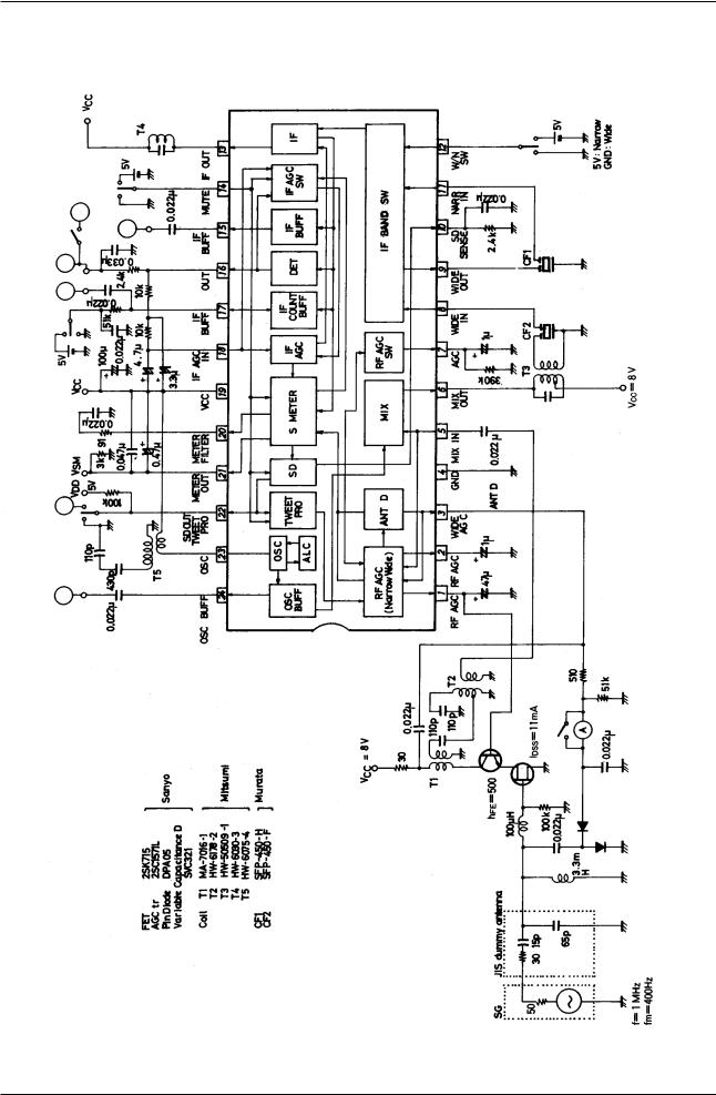
LA1136N, LA1136NM Test Circuit
High frequency IHF signal level meter |
signal level meter with bandpass filter |
Distortion meter |
High frequency signal level meter |
Unit (resistance: Ω, capacitance: F) |
|
|
|
S-meter output |
|
|
Voltmeter |
|
|
|
High frequency |
signal level meter |
|
|
|
No. 3507-5/28
LA1136N, 1136NM, 1137N, 1137NM
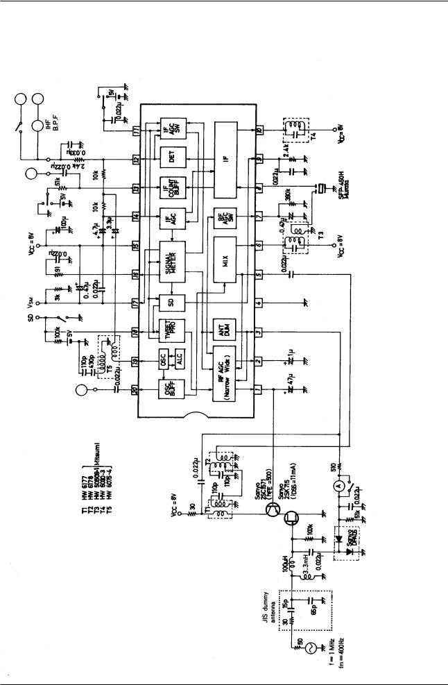
LA1137N, LA1137NM Test Circuit
Distortion meter |
Signal meter |
VHF signal meter |
(resistance: Ω, capacitance: F) |
|
Unit |
S-meter output |
|
VHF signal meter
No. 3507-6/28

LA1136N, 1136NM, 1137N, 1137NM
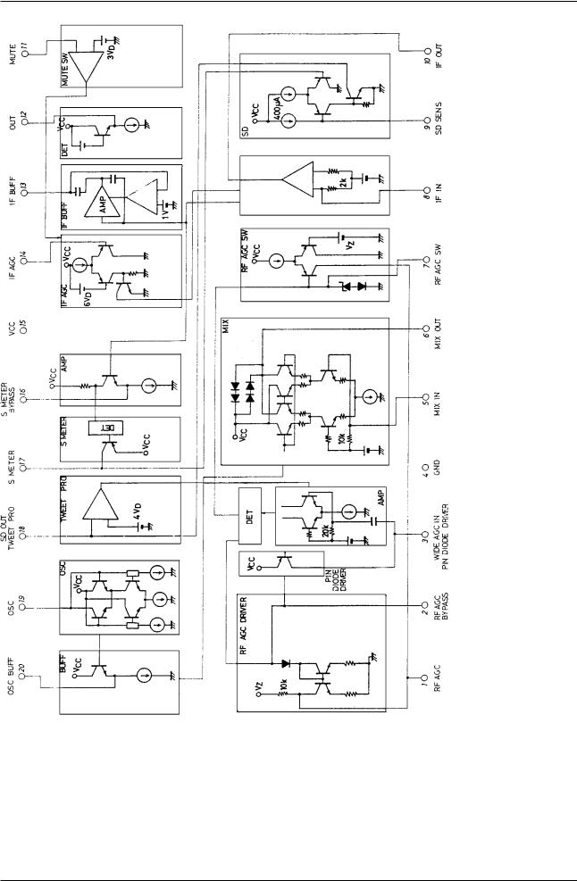
LA1136N Equivalent Circuit
No. 3507-7/28
LA1136N, 1136NM, 1137N, 1137NM
LA1137N Equivalent Circuit
No. 3507-8/28
LA1136N, 1136NM, 1137N, 1137NM
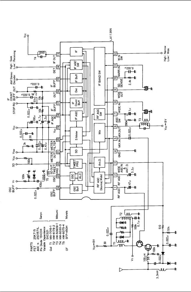
LA1136N Sample Application Circuit
connected to the controller |
Unit (resistance: Ω, capacitance: F) |
Pins |
|
.
No. 3507-9/28
 Loading...