


Philips P51XAG33JB A, P51XAG33JF A, P51XAG33KB A, P51XAG37KF A, P51XAG30JF BD Datasheet
...INTEGRATED CIRCUITS
XA-G3
XA 16-bit microcontroller family
32K/512 OTP/ROM/ROMless, watchdog, 2 UARTs
Product specification |
1998 Aug 14 |
Supersedes data of 1998 Jun 04
IC25 Data Handbook
m n r

Philips Semiconductors Product specification
XA 16-bit microcontroller family |
XA-G3 |
|
32K/512 OTP/ROM/ROMless, watchdog, 2 UARTs |
||
|
||
|
|
|
|
|
FAMILY DESCRIPTION
The Philips Semiconductors XA (eXtended Architecture) family of 16-bit single-chip microcontrollers is powerful enough to easily handle the requirements of high performance embedded applications, yet inexpensive enough to compete in the market for high-volume, low-cost applications.
The XA family provides an upward compatibility path for 80C51 users who need higher performance and 64k or more of program memory. Existing 80C51 code can also easily be translated to run on XA microcontrollers.
The performance of the XA architecture supports the comprehensive bit-oriented operations of the 80C51 while incorporating support for multi-tasking operating systems and high-level languages such as C. The speed of the XA architecture, at 10 to 100 times that of the 80C51, gives designers an easy path to truly high performance embedded control.
The XA architecture supports:
•Upward compatibility with the 80C51 architecture
•16-bit fully static CPU with a 24-bit program and data address range
•Eight 16-bit CPU registers each capable of performing all arithmetic and logic operations as well as acting as memory pointers. Operations may also be performed directly to memory.
•Both 8-bit and 16-bit CPU registers, each capable of performing all arithmetic and logic operations.
•An enhanced instruction set that includes bit intensive logic operations and fast signed or unsigned 16 × 16 multiply and 32 / 16 divide
•Instruction set tailored for high level language support
•Multi-tasking and real-time executives that include up to 32 vectored interrupts, 16 software traps, segmented data memory, and banked registers to support context switching
•Low power operation, which is intrinsic to the XA architecture, includes power-down and idle modes.
More detailed information on the core is available in the XA User Guide.
SPECIFIC FEATURES OF THE XA-G3
•20-bit address range, 1 megabyte each program and data space. (Note that the XA architecture supports up to 24 bit addresses.)
•2.7V to 5.5V operation (EPROM and OTP are 5V ± 5%)
•32K bytes on-chip EPROM/ROM program memory = XA-G37/XA-G33
•512 bytes of on-chip data RAM
•Three counter/timers with enhanced features (equivalent to 80C51 T0, T1, and T2)
•Watchdog timer
•Two enhanced UARTs
•Four 8-bit I/O ports with 4 programmable output configurations
•44-pin PLCC and 44-pin LQFP packages
ORDERING INFORMATION
ROMless |
ROM |
EPROM1 |
|
TEMPERATURE RANGE °C AND PACKAGE |
FREQ |
DRAWING |
|
(MHz) |
NUMBER |
||||
|
|
|
|
|
||
|
|
|
|
|
|
|
P51XAG30JB BD |
P51XAG33JB BD |
P51XAG37JB BD |
OTP |
0 to +70, Plastic Low Profile Quad Flat Pkg. |
25 |
SOT389±1 |
|
|
|
|
|
|
|
P51XAG30JB A |
P51XAG33JB A |
P51XAG37JB A |
OTP |
0 to +70, Plastic Leaded Chip Carrier |
25 |
SOT187±2 |
|
|
|
|
|
|
|
P51XAG30JF BD |
P51XAG33JF BD |
P51XAG37JF BD |
OTP |
±40 to +85, Plastic Low Profile Quad Flat Pkg. |
25 |
SOT389±1 |
|
|
|
|
|
|
|
P51XAG30JF A |
P51XAG33JF A |
P51XAG37JF A |
OTP |
±40 to +85, Plastic Leaded Chip Carrier |
25 |
SOT187±2 |
|
|
|
|
|
|
|
P51XAG30KB BD |
P51XAG33KB BD |
P51XAG37KB BD |
OTP |
0 to +70, Plastic Low Profile Quad Flat Pkg. |
30 |
SOT389±1 |
|
|
|
|
|
|
|
P51XAG30KB A |
P51XAG33KB A |
P51XAG37KB A |
OTP |
0 to +70, Plastic Leaded Chip Carrier |
30 |
SOT187±2 |
|
|
|
|
|
|
|
P51XAG30KF BD |
P51XAG33KF BD |
P51XAG37KF BD |
OTP |
±40 to +85, Plastic Low Profile Quad Flat Pkg. |
30 |
SOT389±1 |
|
|
|
|
|
|
|
P51XAG30KF A |
P51XAG33KF A |
P51XAG37KF A |
OTP |
±40 to +85, Plastic Leaded Chip Carrier |
30 |
SOT187±2 |
|
|
|
|
|
|
|
NOTE:
1. OTP = One Time Programmable EPROM. UV = Erasable EPROM.
1998 Aug 14 |
2 |
853-2052 19875 |
Philips Semiconductors Product specification
XA 16-bit microcontroller family |
XA-G3 |
32K/512 OTP/ROM/ROMless, watchdog, 2 UARTs |
|
|
|
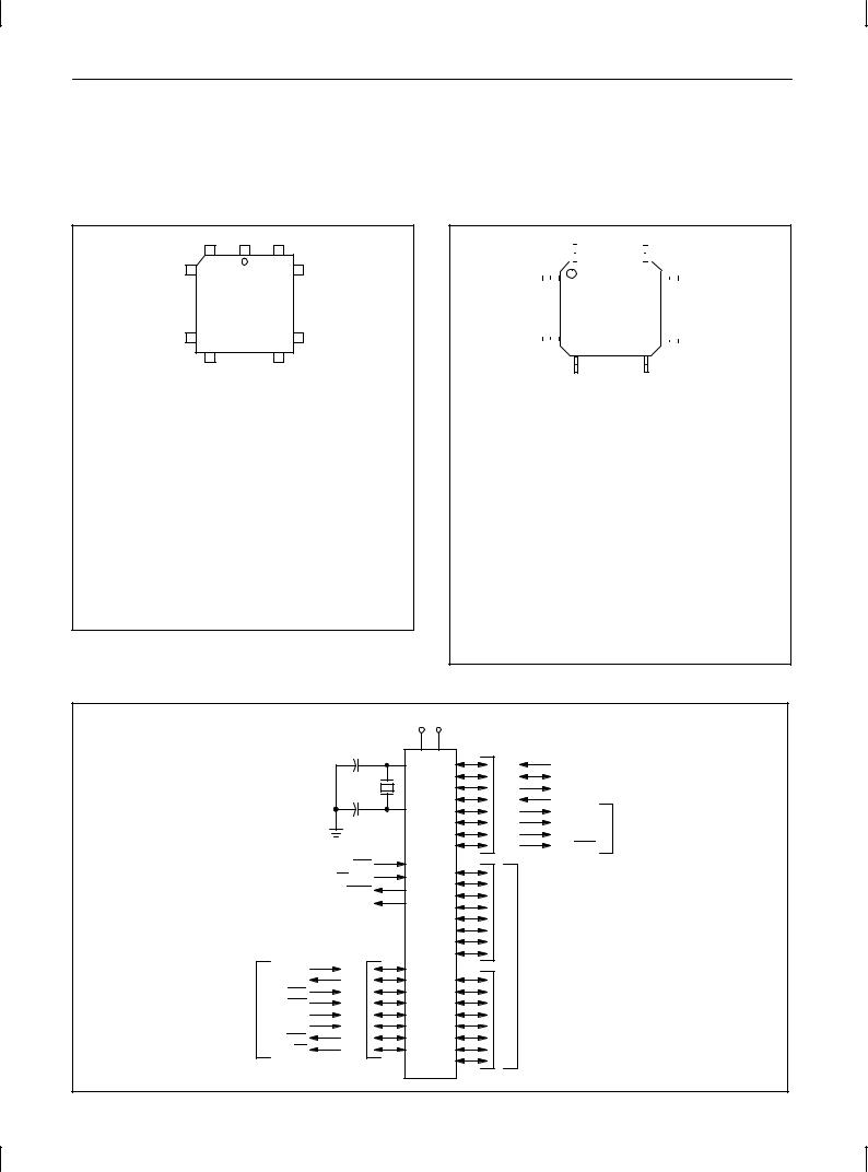
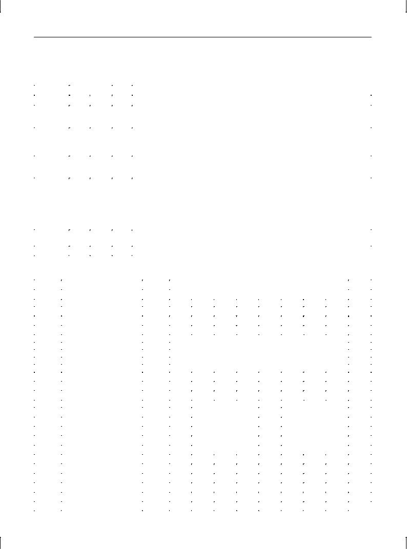
PIN CONFIGURATIONS |
|
44-Pin PLCC Package |
44-Pin LQFP Package |
6 |
1 |
40 |
7 |
|
39 |
|
PLCC |
|
17 |
|
29 |
18 |
|
28 |
Pin |
Function |
Pin |
Function |
|||||||||
1 |
VSS |
|
|
23 |
VDD |
|||||||
2 |
P1.0/A0/WRH |
|
24 |
P2.0/A12D8 |
||||||||
3 |
P1.1/A1 |
25 |
P2.1/A13D9 |
|||||||||
4 |
P1.2/A2 |
26 |
P2.2/A14D10 |
|||||||||
5 |
P1.3/A3 |
27 |
P2.3/A15D11 |
|||||||||
6 |
P1.4/RxD1 |
28 |
P2.4/A16D12 |
|||||||||
7 |
P1.5/TxD1 |
29 |
P2.5/A17D13 |
|||||||||
8 |
P1.6/T2 |
30 |
P2.6/A18D14 |
|||||||||
9 |
P1.7/T2EX |
31 |
P2.7/A19D15 |
|||||||||
10 |
RST |
|
|
|
|
32 |
PSEN |
|
|
|||
11 |
P3.0/RxD0 |
33 |
|
|
|
|
||||||
ALE/PROG |
||||||||||||
12 |
NC |
34 |
NC |
|
||||||||
13 |
P3.1/TxD0 |
35 |
EA/VPP/WAIT |
|||||||||
14 |
|
|
|
|
36 |
P0.7/A11D7 |
||||||
P3.2/INT0 |
||||||||||||
15 |
|
|
|
|
37 |
P0.6/A10D6 |
||||||
P3.3/INT1 |
||||||||||||
16 |
P3.4/T0 |
38 |
P0.5/A9D5 |
|||||||||
17 |
P3.5/T1/BUSW |
39 |
P0.4/A8D4 |
|||||||||
18 |
P3.6/WRL |
|
40 |
P0.3/A7D3 |
||||||||
19 |
|
|
|
41 |
P0.2/A6D2 |
|||||||
P3.7/RD |
|
|||||||||||
20 |
XTAL2 |
42 |
P0.1/A5D1 |
|||||||||
21 |
XTAL1 |
43 |
P0.0/A4D0 |
|||||||||
22 |
VSS |
44 |
VDD |
|||||||||
|
|
|
|
|
|
|
|
|
|
SU00525 |
||
|
44 |
|
34 |
|
|
|
|
|
|
|
|
|||||||||||
|
1 |
|
|
|
|
|
|
|
|
|
|
|
|
|
|
|
|
|
|
33 |
|
|
|
|
|
|
|
|
|
|
|
LQFP |
|
|
|
|
|
|
|
|
|||||
|
|
|
|
|
|
|
|
|
|
|
|
|
|
|
||||||||
|
|
|
|
|
|
|
|
|
|
|
|
|
|
|
|
|
|
|
|
|
|
|
|
11 |
|
|
|
|
|
|
|
|
|
|
|
|
|
|
|
23 |
|
||||
|
|
|
|
|
|
|
|
|
|
|
|
|
|
|
|
|
|
|||||
|
|
|
|
|
|
|
|
|
|
|
|
|
|
|
|
|
|
|||||
|
|
|
|
|
|
|
|
|
|
|
|
|
|
|
|
|||||||
|
12 |
|
22 |
|
|
|
|
|
|
|
|
|||||||||||
Pin |
|
Function |
Pin |
|
|
|
|
Function |
||||||||||||||
1 |
|
P1.5/TxD1 |
23 |
|
|
|
|
P2.5/A17D13 |
||||||||||||||
2 |
|
P1.6/T2 |
24 |
|
|
|
|
P2.6/A18D14 |
||||||||||||||
3 |
|
P1.7/T2EX |
25 |
|
|
|
|
P2.7/A19D15 |
||||||||||||||
4 |
|
|
|
|
|
|
26 |
|
|
|
|
|
|
|
|
|
|
|||||
|
RST |
|
|
|
PSEN |
|||||||||||||||||
5 |
|
P3.0/RxD0 |
27 |
|
|
|
|
|
|
|
|
|
||||||||||
|
|
|
|
|
ALE/PROG |
|||||||||||||||||
6 |
|
NC |
28 |
|
|
|
|
NC |
||||||||||||||
7 |
|
P3.1/TxD0 |
29 |
|
|
|
|
|
|
|
||||||||||||
|
|
|
|
|
EA/VPP/WAIT |
|||||||||||||||||
8 |
|
|
|
|
|
30 |
|
|
|
|
P0.7/A11D7 |
|||||||||||
|
P3.2/INT0 |
|
|
|
||||||||||||||||||
9 |
|
|
|
|
|
31 |
|
|
|
|
P0.6/A10D6 |
|||||||||||
|
P3.3/INT1 |
|
|
|
||||||||||||||||||
10 |
|
P3.4/T0 |
32 |
|
|
|
|
P0.5/A9D5 |
||||||||||||||
11 |
|
P3.5/T1/BUSW |
33 |
|
|
|
|
P0.4/A8D4 |
||||||||||||||
12 |
|
|
|
|
|
34 |
|
|
|
|
P0.3/A7D3 |
|||||||||||
|
P3.6/WRL |
|
|
|
||||||||||||||||||
13 |
|
|
|
|
35 |
|
|
|
|
P0.2/A6D2 |
||||||||||||
|
P3.7/RD |
|
|
|
||||||||||||||||||
14 |
|
XTAL2 |
36 |
|
|
|
|
P0.1/A5D1 |
||||||||||||||
15 |
|
XTAL1 |
37 |
|
|
|
|
P0.0/A4D0 |
||||||||||||||
16 |
|
VSS |
38 |
|
|
|
|
VDD |
||||||||||||||
17 |
|
VDD |
39 |
|
|
|
|
VSS |
|
|||||||||||||
18 |
|
P2.0/A12D8 |
40 |
|
|
|
|
P1.0/A0/WRH |
||||||||||||||
19 |
|
P2.1/A13D9 |
41 |
|
|
|
|
P1.1/A1 |
||||||||||||||
20 |
|
P2.2/A14D10 |
42 |
|
|
|
|
P1.2/A2 |
||||||||||||||
21 |
|
P2.3/A15D11 |
43 |
|
|
|
|
P1.3/A3 |
||||||||||||||
22 |
|
P2.4/A16/D12 |
44 |
|
|
|
|
P1.4/RxD1 |
||||||||||||||
SU00580
LOGIC SYMBOL |
|
|
|
|
|
|
|
VDD |
VSS |
|
|
|
|
XTAL1 |
|
T2EX* |
|
|
|
|
|
|
|
|
|
|
|
T2* |
|
|
|
|
1 |
TXD1 |
|
|
|
|
PORT |
RXD1 |
|
|
|
XTAL2 |
A3 |
ADDRESS BUS |
|
|
|
A0/WRH |
|||
|
|
|
|
A2 |
|
|
|
|
|
A1 |
|
|
|
RST |
|
|
|
|
|
EA/WAIT |
|
|
|
|
|
PSEN |
|
|
|
|
|
ALE |
2 |
|
|
|
|
PORT |
DATA BUS |
|
|
FUNCTIONSALTERNATE |
|
3PORT |
|
||
RxD0 |
0PORT |
ADDRESSAND |
|
||
|
|
|
|
|
|
|
TxD0 |
|
|
|
|
|
INT0 |
|
|
|
|
|
INT1 |
|
|
|
|
|
T0 |
|
|
|
|
|
T1/BUSW |
|
|
|
|
|
WRL |
|
|
|
|
|
RD |
|
|
|
|
* NOT AVAILABLE ON 40-PIN DIP PACKAGE |
|
|
|
SU00526 |
|
|
|
|
|
||
1998 Aug 14 |
|
|
3 |
|
|

Philips Semiconductors Product specification
XA 16-bit microcontroller family |
XA-G3 |
|
32K/512 OTP/ROM/ROMless, watchdog, 2 UARTs |
||
|
||
|
|
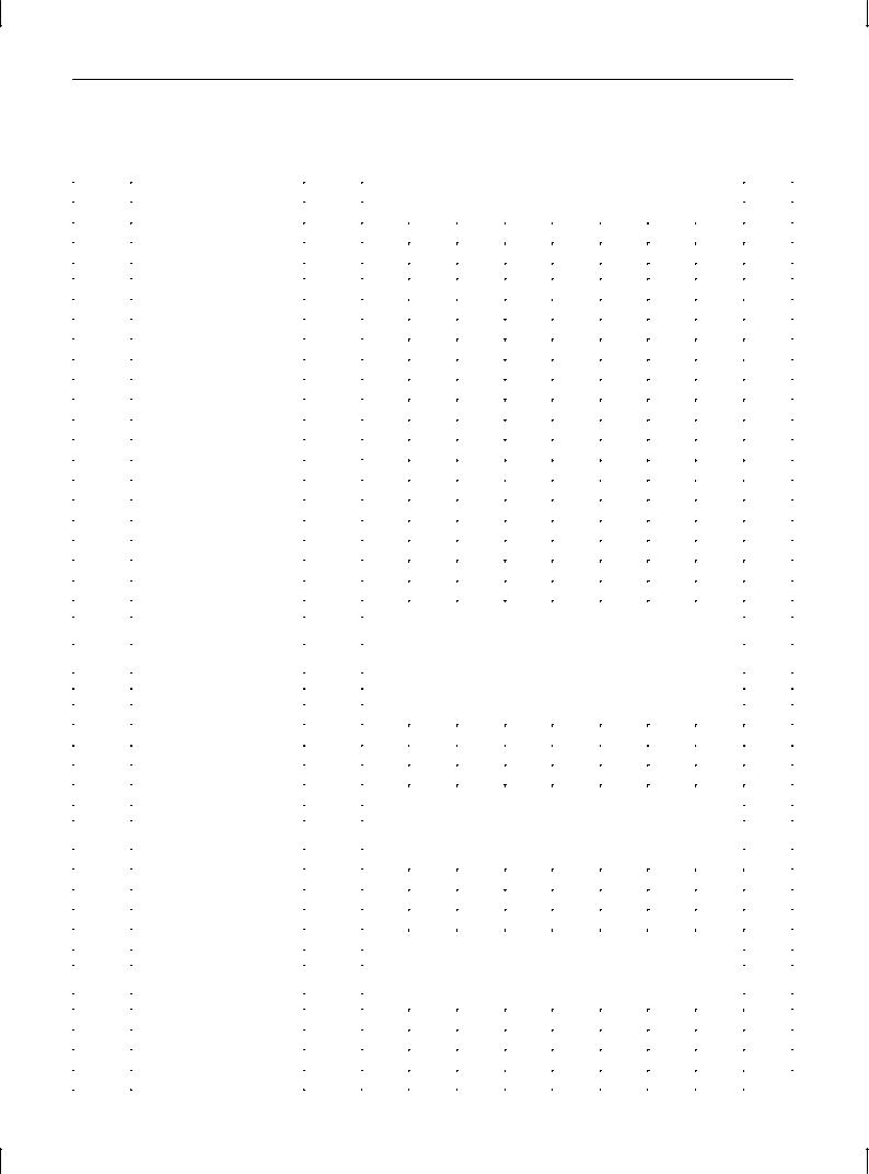
BLOCK DIAGRAM
XA CPU Core |
|
Program |
SFR BUS |
Memory |
|
Bus |
|
32K BYTES |
|
ROM/EPROM |
|
|
UART0 |
Data Bus |
|
512 BYTES |
|
STATIC RAM |
|
|
UART1 |
PORT 0 |
|
|
TIMER 0 & |
|
TIMER 1 |
PORT 1 |
|
|
TIMER 2 |
PORT 2 |
|
|
WATCHDOG |
|
TIMER |
PORT 3 |
|
|
SU00527 |
1998 Aug 14 |
4 |

Philips Semiconductors Product specification
XA 16-bit microcontroller family |
XA-G3 |
||||||||||||
32K/512 OTP/ROM/ROMless, watchdog, 2 UARTs |
|||||||||||||
|
|
|
|
|
|
|
|
|
|
|
|
|
|
PIN DESCRIPTIONS |
|
|
|
|
|
|
|
|
|
|
|
||
|
|
|
|
|
|
|
|
|
|
|
|
|
|
MNEMONIC |
PIN. NO. |
TYPE |
|
|
|
|
|
|
|
|
|
NAME AND FUNCTION |
|
|
|
|
|
|
|
|
|
|
|
|
|||
PLCC |
LQFP |
|
|
|
|
|
|
|
|
|
|||
|
|
|
|
|
|
|
|
|
|
|
|
||
|
|
|
|
|
|
|
|
|
|
|
|
|
|
VSS |
1, 22 |
16 |
I |
Ground: 0V reference. |
|||||||||
VDD |
23, 44 |
17 |
I |
Power Supply: This is the power supply voltage for normal, idle, and power down operation. |
|||||||||
P0.0 ± P0.7 |
43±36 |
37±30 |
I/O |
Port 0: Port 0 is an 8-bit I/O port with a user-configurable output type. Port 0 latches have 1s |
|||||||||
|
|
|
|
written to them and are configured in the quasi-bidirectional mode during reset. The operation of |
|||||||||
|
|
|
|
port 0 pins as inputs and outputs depends upon the port configuration selected. Each port pin is |
|||||||||
|
|
|
|
configured independently. Refer to the section on I/O port configuration and the DC Electrical |
|||||||||
|
|
|
|
Characteristics for details. |
|||||||||
|
|
|
|
When the external program/data bus is used, Port 0 becomes the multiplexed low data/instruction |
|||||||||
|
|
|
|
byte and address lines 4 through 11. |
|||||||||
|
|
|
|
Port 0 also outputs the code bytes during program verification and receives code bytes during |
|||||||||
|
|
|
|
EPROM programming. |
|||||||||
|
|
|
|
|
|
|
|
|
|
|
|
|
|
P1.0 ± P1.7 |
2±9 |
40±44, |
I/O |
Port 1: Port 1 is an 8-bit I/O port with a user-configurable output type. Port 1 latches have 1s |
|||||||||
|
|
1±3 |
|
written to them and are configured in the quasi-bidirectional mode during reset. The operation of |
|||||||||
|
|
|
|
port 1 pins as inputs and outputs depends upon the port configuration selected. Each port pin is |
|||||||||
|
|
|
|
configured independently. Refer to the section on I/O port configuration and the DC Electrical |
|||||||||
|
|
|
|
Characteristics for details. |
|||||||||
|
|
|
|
Port 1 also provides special functions as described below. |
|||||||||
|
2 |
40 |
O |
|
|
|
|
|
|
|
|
|
Address bit 0 of the external address bus when the external data bus is |
|
|
A0/WRH: |
|
||||||||||
|
|
|
|
|
|
|
|
|
|
|
|
|
configured for an 8 bit width. When the external data bus is configured for a 16 |
|
|
|
|
|
|
|
|
|
|
|
|
|
bit width, this pin becomes the high byte write strobe. |
|
3 |
41 |
O |
|
A1: |
Address bit 1 of the external address bus. |
|||||||
|
4 |
42 |
O |
|
A2: |
Address bit 2 of the external address bus. |
|||||||
|
5 |
43 |
O |
|
A3: |
Address bit 3 of the external address bus. |
|||||||
|
6 |
44 |
I |
|
RxD1 (P1.4): |
Receiver input for serial port 1. |
|||||||
|
7 |
1 |
O |
|
TxD1 (P1.5): |
Transmitter output for serial port 1. |
|||||||
|
8 |
2 |
I/O |
|
T2 (P1.6): |
Timer/counter 2 external count input/clockout. |
|||||||
|
9 |
3 |
I |
|
T2EX (P1.7): Timer/counter 2 reload/capture/direction control |
||||||||
|
|
|
|
|
|
|
|
|
|
|
|||
P2.0 ± P2.7 |
24±31 |
18±25 |
I/O |
Port 2: Port 2 is an 8-bit I/O port with a user-configurable output type. Port 2 latches have 1s |
|||||||||
|
|
|
|
written to them and are configured in the quasi-bidirectional mode during reset. The operation of |
|||||||||
|
|
|
|
port 2 pins as inputs and outputs depends upon the port configuration selected. Each port pin is |
|||||||||
|
|
|
|
configured independently. Refer to the section on I/O port configuration and the DC Electrical |
|||||||||
|
|
|
|
Characteristics for details. |
|||||||||
|
|
|
|
When the external program/data bus is used in 16-bit mode, Port 2 becomes the multiplexed high |
|||||||||
|
|
|
|
data/instruction byte and address lines 12 through 19. When the external program/data bus is used in |
|||||||||
|
|
|
|
8-bit mode, the number of address lines that appear on port 2 is user programmable. |
|||||||||
|
|
|
|
Port 2 also receives the low-order address byte during program memory verification. |
|||||||||
|
|
|
|
|
|
|
|
|
|
|
|||
P3.0 ± P3.7 |
11, |
5, |
I/O |
Port 3: Port 3 is an 8-bit I/O port with a user configurable output type. Port 3 latches have 1s |
|||||||||
|
13±19 |
7±13 |
|
written to them and are configured in the quasi-bidirectional mode during reset. the operation of |
|||||||||
|
|
|
|
port 3 pins as inputs and outputs depends upon the port configuration selected. Each port pin is |
|||||||||
|
|
|
|
configured independently. Refer to the section on I/O port configuration and the DC Electrical |
|||||||||
|
|
|
|
Characteristics for details. |
|||||||||
|
|
|
|
Port 3 pins receive the high order address bits during EPROM programming and verification. |
|||||||||
|
|
|
|
Port 3 also provides various special functions as described below. |
|||||||||
|
11 |
5 |
I |
|
RxD0 (P3.0): |
Receiver input for serial port 0. |
|||||||
|
13 |
7 |
O |
|
TxD0 (P3.1): |
Transmitter output for serial port 0. |
|||||||
|
14 |
8 |
I |
|
|
|
|
|
|
(P3.2): |
External interrupt 0 input. |
||
|
|
INT0 |
|||||||||||
|
15 |
9 |
I |
|
|
|
|
|
(P3.3): |
External interrupt 1 input. |
|||
|
|
INT1 |
|||||||||||
|
16 |
10 |
I/O |
|
T0 (P3.4): |
Timer 0 external input, or timer 0 overflow output. |
|||||||
|
17 |
11 |
I/O |
|
T1/BUSW (P3.5): Timer 1 external input, or timer 1 overflow output. The value on this pin is |
||||||||
|
|
|
|
|
|
|
|
|
|
|
|
|
latched as the external reset input is released and defines the default |
|
|
|
|
|
|
|
|
|
|
|
|
|
external data bus width (BUSW). 0 = 8-bit bus and 1 = 16-bit bus. |
|
18 |
12 |
O |
|
|
|
|
(P3.6): |
External data memory low byte write strobe. |
||||
|
|
WRL |
|||||||||||
|
19 |
13 |
O |
|
|
(P3.7): |
External data memory read strobe. |
||||||
|
|
RD |
|||||||||||
1998 Aug 14 |
5 |
Philips Semiconductors Product specification
|
XA 16-bit microcontroller family |
|
|
|
|
|
|
|
|
|
|
XA-G3 |
|||||||||||||||||||
|
32K/512 OTP/ROM/ROMless, watchdog, 2 UARTs |
|
|
|
|
|
|
||||||||||||||||||||||||
|
|
|
|
|
|
|
|
|
|
|
|
|
|||||||||||||||||||
|
|
|
|
|
|
|
|
|
|
|
|
|
|
|
|
|
|
|
|
|
|
|
|
|
|
|
|
|
|
|
|
|
|
|
|
|
|
|
|
|
|
|
|
|
|
|
|
|
|
|
|
|
|
|
|
|
|
|
|
|
|
|
|
MNEMONIC |
PIN. NO. |
TYPE |
|
|
|
|
|
NAME AND FUNCTION |
|
|
|
|
|
|
|
|
|||||||||||||||
|
|
|
|
|
|
|
|
|
|
|
|
|
|
|
|||||||||||||||||
PLCC |
LQFP |
|
|
|
|
|
|
|
|
|
|
|
|
||||||||||||||||||
|
|
|
|
|
|
|
|
|
|
|
|
|
|
|
|
|
|
|
|
|
|
|
|
|
|
|
|
|
|
||
|
|
|
|
|
|
|
|
|
|
|
|
|
|
|
|
|
|
|
|
|
|
|
|
|
|
|
|
|
|
|
|
|
|
|
|
|
|
|
|
|
|
|
10 |
4 |
I |
Reset: A low on this pin resets the microcontroller, causing I/O ports and peripherals to take on |
|||||||||||||||||
|
|
|
RST |
|
|
||||||||||||||||||||||||||
|
|
|
|
|
|
|
|
|
|
|
|
|
|
their default states, and the processor to begin execution at the address contained in the reset |
|||||||||||||||||
|
|
|
|
|
|
|
|
|
|
|
|
|
|
vector. Refer to the section on Reset for details. |
|
|
|
|
|
|
|
|
|
|
|
||||||
|
|
|
|
|
|
|
|
|
|
|
|
|
|
|
|
|
|
|
|
|
|
|
|
|
|
|
|||||
|
|
|
|
|
|
|
|
|
|
|
33 |
27 |
I/O |
Address Latch Enable/Program Pulse: A high output on the ALE pin signals external circuitry to |
|||||||||||||||||
ALE/PROG |
|||||||||||||||||||||||||||||||
|
|
|
|
|
|
|
|
|
|
|
|
|
|
latch the address portion of the multiplexed address/data bus. A pulse on ALE occurs only when it |
|||||||||||||||||
|
|
|
|
|
|
|
|
|
|
|
|
|
|
is needed in order to process a bus cycle. During EPROM programming, this pin is used as the |
|||||||||||||||||
|
|
|
|
|
|
|
|
|
|
|
|
|
|
program pulse input. |
|
|
|
|
|
|
|
|
|
|
|
|
|
|
|
||
|
|
|
|
|
|
|
|
|
|
|
|
|
|
|
|
|
|
|
|
|
|
|
|
|
|
|
|
||||
|
|
|
|
|
|
|
|
|
|
|
32 |
26 |
O |
Program Store Enable: The read strobe for external program memory. When the microcontroller |
|||||||||||||||||
PSEN |
|
|
|||||||||||||||||||||||||||||
|
|
|
|
|
|
|
|
|
|
|
|
|
|
accesses external program memory, |
PSEN |
is driven low in order to enable memory devices. |
PSEN |
|
|||||||||||||
|
|
|
|
|
|
|
|
|
|
|
|
|
|
is only active when external code accesses are performed. |
|
|
|
|
|
|
|
|
|||||||||
|
|
|
|
|
|
|
|
|
|
|
|
|
|
|
|
|
|
|
|
|
|
||||||||||
|
|
|
|
|
|
|
|
|
|
|
35 |
29 |
I |
External Access/Wait/Programming Supply Voltage: The |
|
|
input determines whether the |
||||||||||||||
|
EA/WAIT/ |
|
|
EA |
|||||||||||||||||||||||||||
|
|
|
VPP |
|
|
|
|
|
internal program memory of the microcontroller is used for code execution. The value on the |
EA |
pin |
||||||||||||||||||||
|
|
|
|
|
|
|
|
|
|
|
|
|
|
is latched as the external reset input is released and applies during later execution. When latched |
|||||||||||||||||
|
|
|
|
|
|
|
|
|
|
|
|
|
|
as a 0, external program memory is used exclusively, when latched as a 1, internal program |
|
|
|
|
|||||||||||||
|
|
|
|
|
|
|
|
|
|
|
|
|
|
memory will be used up to its limit, and external program memory used above that point. After reset |
|||||||||||||||||
|
|
|
|
|
|
|
|
|
|
|
|
|
|
is released, this pin takes on the function of bus Wait input. If Wait is asserted high during any |
|||||||||||||||||
|
|
|
|
|
|
|
|
|
|
|
|
|
|
external bus access, that cycle will be extended until Wait is released. During EPROM |
|
|
|
|
|||||||||||||
|
|
|
|
|
|
|
|
|
|
|
|
|
|
programming, this pin is also the programming supply voltage input. |
|
|
|
|
|
|
|
||||||||||
|
|
|
|
|
|
|
|
|
|
|
|
|
|
|
|
|
|
|
|||||||||||||
|
XTAL1 |
|
|
21 |
15 |
I |
Crystal 1: Input to the inverting amplifier used in the oscillator circuit and input to the internal clock |
||||||||||||||||||||||||
|
|
|
|
|
|
|
|
|
|
|
|
|
|
generator circuits. |
|
|
|
|
|
|
|
|
|
|
|
|
|
|
|
||
|
|
|
|
|
|
|
|
|
|
|
|
|
|
|
|
|
|
|
|
|
|
|
|
|
|||||||
|
XTAL2 |
|
|
20 |
14 |
O |
Crystal 2: Output from the oscillator amplifier. |
|
|
|
|
|
|
|
|
|
|
|
|||||||||||||
|
|
|
|
|
|
|
|
|
|
|
|
|
|
|
|
|
|
|
|
|
|
|
|
|
|
|
|
|
|
|
|
SPECIAL FUNCTION REGISTERS |
|
|
|
|
|
|
|
|
|
|
|
|
|
|
|
|
|||||||||||||||
|
|
|
|
|
|
|
|
|
|
|
|
|
|
|
|
|
|
|
|
|
|
|
|
|
|
|
|
|
|||
NAME |
|
|
|
DESCRIPTION |
|
SFR |
|
|
BIT FUNCTIONS AND ADDRESSES |
|
|
|
RESET |
||||||||||||||||||
|
|
|
|
|
|
|
|
|
|
|
|
|
|
|
|
||||||||||||||||
|
|
|
|
ADDRESS |
MSB |
|
|
|
|
|
|
|
|
|
LSB |
|
VALUE |
||||||||||||||
|
|
|
|
|
|
|
|
|
|
|
|
|
|
|
|
|
|
|
|
|
|
|
|
|
|||||||
|
|
|
|
|
|
|
|
|
|
|
|
|
|
|
|
|
|
|
|
|
|
|
|
|
|
|
|
|
|
||
|
|
|
|
|
|
|
|
|
|
|
|
|
|
|
|
||||||||||||||||
|
|
|
|
|
|
|
|
|
|
|
|
|
|
|
|
||||||||||||||||
BCR |
|
Bus configuration register |
|
46A |
Ð |
Ð |
Ð |
WAITD |
BUSD |
|
BC2 |
BC1 |
BC0 |
|
Note 1 |
||||||||||||||||
|
|
|
|
|
|
|
|
|
|
|
|
|
|
|
|
|
|||||||||||||||
BTRH |
|
Bus timing register high byte |
|
469 |
DW1 |
DW0 |
DWA1 |
DWA0 |
DR1 |
|
DR0 |
DRA1 |
DRA0 |
|
|
FF |
|||||||||||||||
|
|
|
|
|
|
|
|
|
|
|
|
|
|
|
|
|
|||||||||||||||
BTRL |
|
Bus timing register low byte |
|
468 |
WM1 |
WM0 |
ALEW |
Ð |
CR1 |
|
CR0 |
CRA1 |
CRA0 |
|
|
EF |
|||||||||||||||
CS |
|
Code segment |
|
|
443 |
|
|
|
|
|
|
|
|
|
|
|
|
00 |
|
||||||||||||
|
|
|
|
|
|
|
|
|
|
|
|
|
|
|
|
||||||||||||||||
DS |
|
Data segment |
|
|
441 |
|
|
|
|
|
|
|
|
|
|
|
|
00 |
|
||||||||||||
ES |
|
Extra segment |
|
|
442 |
|
|
|
|
|
|
|
|
|
|
|
|
00 |
|
||||||||||||
|
|
|
|
|
|
|
|
|
|
|
|
|
|
|
|
33F |
33E |
33D |
33C |
33B |
33A |
339 |
338 |
|
|
|
|
|
|||
|
|
|
|
|
|
|
|
|
|
|
|
|
|
|
|
||||||||||||||||
IEH* |
|
Interrupt enable high byte |
|
427 |
Ð |
Ð |
Ð |
Ð |
ETI1 |
|
ERI1 |
ETI0 |
ERI0 |
|
00 |
|
|||||||||||||||
|
|
|
|
|
|
|
|
|
|
|
|
|
|
|
|
|
|
|
|
|
|
|
|
|
|
|
|
|
|
|
|
|
|
|
|
|
|
|
|
|
|
|
|
|
|
|
|
337 |
336 |
335 |
334 |
333 |
|
|
332 |
331 |
330 |
|
|
|
|
|
|
|
|
|
|
|
|
|
|
|
|
|
|
|
|
|
|
||||||||||||||||
IEL* |
|
Interrupt enable low byte |
|
426 |
EA |
Ð |
Ð |
ET2 |
ET1 |
|
EX1 |
ET0 |
EX0 |
|
00 |
|
|||||||||||||||
|
|
|
|
|
|
|
|
|
|
|
|
|
|
|
|
|
|
|
|||||||||||||
|
|
|
|
|
|
|
|
|
|
|
|
|
|
|
|
|
|
|
|||||||||||||
IPA0 |
|
Interrupt priority 0 |
|
|
4A0 |
Ð |
|
PT0 |
|
Ð |
|
|
|
PX0 |
|
|
00 |
|
|||||||||||||
|
|
|
|
|
|
|
|
|
|
|
|
|
|
|
|
|
|
|
|||||||||||||
IPA1 |
|
Interrupt priority 1 |
|
|
4A1 |
Ð |
|
PT1 |
|
Ð |
|
|
|
PX1 |
|
|
00 |
|
|||||||||||||
|
|
|
|
|
|
|
|
|
|
|
|
|
|
|
|
|
|
|
|||||||||||||
IPA2 |
|
Interrupt priority 2 |
|
|
4A2 |
Ð |
|
Ð |
|
Ð |
|
|
|
PT2 |
|
|
00 |
|
|||||||||||||
|
|
|
|
|
|
|
|
|
|
|
|
|
|
|
|
|
|
|
|||||||||||||
IPA4 |
|
Interrupt priority 4 |
|
|
4A4 |
Ð |
|
PTI0 |
|
Ð |
|
|
|
PRI0 |
|
|
00 |
|
|||||||||||||
|
|
|
|
|
|
|
|
|
|
|
|
|
|
|
|
|
|
|
|||||||||||||
IPA5 |
|
Interrupt priority 5 |
|
|
4A5 |
Ð |
|
PTI1 |
|
Ð |
|
|
|
PRI1 |
|
|
00 |
|
|||||||||||||
|
|
|
|
|
|
|
|
|
|
|
|
|
|
|
|
|
|
|
|
|
|
|
|
|
|
|
|
|
|
|
|
|
|
|
|
|
|
|
|
|
|
|
|
|
|
|
|
387 |
386 |
385 |
384 |
383 |
|
|
382 |
381 |
380 |
|
|
|
|
|
|
|
|
|
|
|
|
|
|
|
|
|
|
|
|
|
|
|
|
||||||||||||||
P0* |
|
Port 0 |
|
|
|
430 |
AD7 |
AD6 |
AD5 |
AD4 |
AD3 |
|
AD2 |
AD1 |
AD0 |
|
|
FF |
|||||||||||||
|
|
|
|
|
|
|
|
|
|
|
|
|
|
|
|
|
|
|
|
|
|
|
|
|
|
|
|
|
|
||
|
|
|
|
|
|
|
|
|
|
|
|
|
|
|
|
38F |
38E |
38D |
38C |
38B |
38A |
389 |
388 |
|
|
|
|
|
|||
|
|
|
|
|
|
|
|
|
|
|
|
|
|
|
|
|
|
||||||||||||||
P1* |
|
Port 1 |
|
|
|
431 |
T2EX |
T2 |
TxD1 |
RxD1 |
A3 |
|
A2 |
A1 |
WRH |
|
|
FF |
|||||||||||||
|
|
|
|
|
|
|
|
|
|
|
|
|
|
|
|
|
|
|
|
|
|
|
|
|
|
|
|
|
|
|
|
|
|
|
|
|
|
|
|
|
|
|
|
|
|
|
|
397 |
396 |
395 |
394 |
393 |
|
|
392 |
391 |
390 |
|
|
|
|
|
|
|
|
|
|
|
|
|
|
|
|
|
|
|
|
|
|
|
|
||||||||||||||
P2* |
|
Port 2 |
|
|
|
432 |
P2.7 |
P2.6 |
P2.5 |
P2.4 |
P2.3 |
|
P2.2 |
P2.1 |
P2.0 |
|
|
FF |
|||||||||||||
|
|
|
|
|
|
|
|
|
|
|
|
|
|
|
|
|
|
|
|
|
|
|
|
|
|
|
|
|
|
|
|
1998 Aug 14 |
6 |
Philips Semiconductors Product specification
XA 16-bit microcontroller family |
XA-G3 |
|
32K/512 OTP/ROM/ROMless, watchdog, 2 UARTs |
||
|
||
|
|
NAME |
DESCRIPTION |
SFR |
|
|
BIT FUNCTIONS AND ADDRESSES |
|
|
RESET |
|||
|
|
|
|
|
|
|
|
||||
ADDRESS |
MSB |
|
|
|
|
|
|
LSB |
VALUE |
||
|
|
|
|
|
|
|
|
||||
|
|
|
|
|
|
|
|
|
|
||
|
|
|
|
|
|
|
|
|
|
|
|
|
|
|
39F |
39E |
39D |
39C |
39B |
39A |
399 |
398 |
|
|
|
|
|
|
|
|
|
|
|
|
|
P3* |
Port 3 |
433 |
RD |
WR |
T1 |
T0 |
INT1 |
INT0 |
TxD0 |
RxD0 |
FF |
P0CFGA |
Port 0 configuration A |
470 |
|
|
|
|
|
|
|
|
Note 5 |
|
|
|
|
|
|
|
|
||||
|
|
|
|
|
|
|
|
||||
P1CFGA |
Port 1 configuration A |
471 |
|
|
|
|
|
|
|
|
Note 5 |
|
|
|
|
|
|
|
|
||||
P2CFGA |
Port 2 configuration A |
472 |
|
|
|
|
|
|
|
|
Note 5 |
|
|
|
|
|
|
|
|
||||
P3CFGA |
Port 3 configuration A |
473 |
|
|
|
|
|
|
|
|
Note 5 |
|
|
|
|
|
|
|
|
||||
P0CFGB |
Port 0 configuration B |
4F0 |
|
|
|
|
|
|
|
|
Note 5 |
|
|
|
|
|
|
|
|
||||
P1CFGB |
Port 1 configuration B |
4F1 |
|
|
|
|
|
|
|
|
Note 5 |
|
|
|
|
|
|
|
|
||||
P2CFGB |
Port 2 configuration B |
4F2 |
|
|
|
|
|
|
|
|
Note 5 |
|
|
|
|
|
|
|
|
||||
P3CFGB |
Port 3 configuration B |
4F3 |
|
|
|
|
|
|
|
|
Note 5 |
|
|
|
|
|
|
|
|
||||
|
|
|
|
|
|
|
|
|
|
|
|
|
|
|
227 |
226 |
225 |
224 |
223 |
222 |
221 |
220 |
|
|
|
|
|
|
|
|
|
|
|
|
|
PCON* |
Power control register |
404 |
Ð |
Ð |
Ð |
Ð |
Ð |
Ð |
PD |
IDL |
00 |
|
|
|
|
|
|
|
|
|
|
|
|
|
|
|
20F |
20E |
20D |
20C |
20B |
20A |
209 |
208 |
|
|
|
|
|
|
|
|
|
|
|
|
|
PSWH* |
Program status word (high byte) |
401 |
SM |
TM |
RS1 |
RS0 |
IM3 |
IM2 |
IM1 |
IM0 |
Note 2 |
|
|
|
|
|
|
|
|
|
|
|
|
|
|
|
207 |
206 |
205 |
204 |
203 |
202 |
201 |
200 |
|
|
|
|
|
|
|
|
|
|
|
|
|
PSWL* |
Program status word (low byte) |
400 |
C |
AC |
Ð |
Ð |
Ð |
V |
N |
Z |
Note 2 |
|
|
|
|
|
|
|
|
|
|
|
|
|
|
|
217 |
216 |
215 |
214 |
213 |
212 |
211 |
210 |
|
|
|
|
|
|
|
|
|
|
|
|
|
PSW51* |
80C51 compatible PSW |
402 |
C |
AC |
F0 |
RS1 |
RS0 |
V |
F1 |
P |
Note 3 |
RTH0 |
Timer 0 extended reload, |
455 |
|
|
|
|
|
|
|
|
00 |
|
|
|
|
|
|
|
|
||||
|
high byte |
|
|
|
|
|
|
|
|
|
|
RTH1 |
Timer 1 extended reload, |
457 |
|
|
|
|
|
|
|
|
00 |
|
high byte |
|
|
|
|
|
|
|
|
|
|
RTL0 |
Timer 0 extended reload, low byte |
454 |
|
|
|
|
|
|
|
|
00 |
RTL1 |
Timer 1 extended reload, low byte |
456 |
|
|
|
|
|
|
|
|
00 |
|
|
|
307 |
306 |
305 |
304 |
303 |
302 |
301 |
300 |
|
|
|
|
|
|
|
|
|
|
|||
S0CON* |
Serial port 0 control register |
420 |
SM0_0 |
SM1_0 |
SM2_0 |
REN_0 |
TB8_0 |
RB8_0 |
TI_0 |
RI_0 |
00 |
|
|
|
|
|
|
|
|
|
|
|
|
|
|
|
30F |
30E |
30D |
30C |
30B |
30A |
309 |
308 |
|
|
|
|
|
|
|
|
|
|
|
|
|
S0STAT* |
Serial port 0 extended status |
421 |
Ð |
Ð |
Ð |
Ð |
FE0 |
BR0 |
OE0 |
STINT0 |
00 |
S0BUF |
Serial port 0 buffer register |
460 |
|
|
|
|
|
|
|
|
x |
|
|
|
|
|
|
|
|
||||
S0ADDR |
Serial port 0 address register |
461 |
|
|
|
|
|
|
|
|
00 |
S0ADEN |
Serial port 0 address enable |
462 |
|
|
|
|
|
|
|
|
00 |
|
register |
|
|
|
|
|
|
|
|
|
|
|
|
|
327 |
326 |
325 |
324 |
323 |
322 |
321 |
320 |
|
|
|
|
|
|
|
|
|
|
|||
S1CON* |
Serial port 1 control register |
424 |
SM0_1 |
SM1_1 |
SM2_1 |
REN_1 |
TB8_1 |
RB8_1 |
TI_1 |
RI_1 |
00 |
|
|
|
|
|
|
|
|
|
|
|
|
|
|
|
32F |
32E |
32D |
32C |
32B |
32A |
329 |
328 |
|
|
|
|
|
|
|
|
|
|
|
|
|
S1STAT* |
Serial port 1 extended status |
425 |
Ð |
Ð |
Ð |
Ð |
FE1 |
BR1 |
OE1 |
STINT1 |
00 |
S1BUF |
Serial port 1 buffer register |
464 |
|
|
|
|
|
|
|
|
x |
|
|
|
|
|
|
|
|
||||
S1ADDR |
Serial port 1 address register |
465 |
|
|
|
|
|
|
|
|
00 |
S1ADEN |
Serial port 1 address enable |
466 |
|
|
|
|
|
|
|
|
00 |
|
register |
|
|
|
|
|
|
|
|
|
|
|
|
|
|
|
|
|
|
|
|
|
|
SCR |
System configuration register |
440 |
Ð |
Ð |
Ð |
Ð |
PT1 |
PT0 |
CM |
PZ |
00 |
|
|
|
|
|
|
|
|
|
|
|
|
|
|
|
21F |
21E |
21D |
21C |
21B |
21A |
219 |
218 |
|
SSEL* |
Segment selection register |
403 |
|
|
|
|
00 |
||||
ESWEN |
R6SEG |
R5SEG |
R4SEG |
R3SEG |
R2SEG |
R1SEG |
R0SEG |
||||
|
|
|
|
|
|
|
|
|
|
|
|
SWE |
Software Interrupt Enable |
47A |
Ð |
SWE7 |
SWE6 |
SWE5 |
SWE4 |
SWE3 |
SWE2 |
SWE1 |
00 |
|
|
|
|
|
|
|
|
|
|
|
|
1998 Aug 14 |
7 |

Philips Semiconductors Product specification
XA 16-bit microcontroller family |
|
|
|
|
|
|
|
XA-G3 |
|||
32K/512 OTP/ROM/ROMless, watchdog, 2 UARTs |
|
|
|
|
|||||||
|
|
|
|
|
|
||||||
|
|
|
|
|
|
|
|
|
|
|
|
|
|
|
|
|
|
|
|
|
|
|
|
NAME |
DESCRIPTION |
SFR |
|
|
BIT FUNCTIONS AND ADDRESSES |
|
|
RESET |
|||
|
|
|
|
|
|
|
|
||||
ADDRESS |
MSB |
|
|
|
|
|
|
LSB |
VALUE |
||
|
|
|
|
|
|
|
|
||||
|
|
|
|
|
|
|
|
|
|
||
|
|
|
|
|
|
|
|
|
|
|
|
|
|
|
357 |
356 |
355 |
354 |
353 |
352 |
351 |
350 |
|
|
|
|
|
|
|
|
|
|
|
|
|
SWR* |
Software Interrupt Request |
42A |
Ð |
SWR7 |
SWR6 |
SWR5 |
SWR4 |
SWR3 |
SWR2 |
SWR1 |
00 |
|
|
|
|
|
|
|
|
|
|
|
|
|
|
|
2C7 |
2C6 |
2C5 |
2C4 |
2C3 |
2C2 |
2C1 |
2C0 |
|
|
|
|
|
|
|
|
|
|
|
|
|
T2CON* |
Timer 2 control register |
418 |
TF2 |
EXF2 |
RCLK0 |
TCLK0 |
EXEN2 |
TR2 |
C/T2 |
CP/RL2 |
00 |
|
|
|
|
|
|
|
|
|
|
|
|
|
|
|
2CF |
2CE |
2CD |
2CC |
2CB |
2CA |
2C9 |
2C8 |
|
|
|
|
|
|
|
|
|
|
|
|
|
T2MOD* |
Timer 2 mode control |
419 |
Ð |
Ð |
RCLK1 |
TCLK1 |
Ð |
Ð |
T2OE |
DCEN |
00 |
TH2 |
Timer 2 high byte |
459 |
|
|
|
|
|
|
|
|
00 |
|
|
|
|
|
|
|
|
||||
TL2 |
Timer 2 low byte |
458 |
|
|
|
|
|
|
|
|
00 |
T2CAPH |
Timer 2 capture register, |
45B |
|
|
|
|
|
|
|
|
00 |
|
high byte |
|
|
|
|
|
|
|
|
|
|
T2CAPL |
Timer 2 capture register, |
45A |
|
|
|
|
|
|
|
|
00 |
|
low byte |
|
|
|
|
|
|
|
|
|
|
|
|
|
287 |
286 |
285 |
284 |
283 |
282 |
281 |
280 |
|
|
|
|
|
|
|
|
|
|
|
|
|
TCON* |
Timer 0 and 1 control register |
410 |
TF1 |
TR1 |
TF0 |
TR0 |
IE1 |
IT1 |
IE0 |
IT0 |
00 |
TH0 |
Timer 0 high byte |
451 |
|
|
|
|
|
|
|
|
00 |
|
|
|
|
|
|
|
|
||||
TH1 |
Timer 1 high byte |
453 |
|
|
|
|
|
|
|
|
00 |
TL0 |
Timer 0 low byte |
450 |
|
|
|
|
|
|
|
|
00 |
TL1 |
Timer 1 low byte |
452 |
|
|
|
|
|
|
|
|
00 |
|
|
|
|
|
|
|
|
|
|
|
|
TMOD |
Timer 0 and 1 mode control |
45C |
GATE |
C/T |
M1 |
M0 |
GATE |
C/T |
M1 |
M0 |
00 |
|
|
|
|
|
|
|
|
|
|
|
|
|
|
|
28F |
28E |
28D |
28C |
28B |
28A |
289 |
288 |
|
|
|
|
|
|
|
|
|
|
|
|
|
TSTAT* |
Timer 0 and 1 extended status |
411 |
Ð |
Ð |
Ð |
Ð |
Ð |
T1OE |
Ð |
T0OE |
00 |
|
|
|
|
|
|
|
|
|
|
|
|
|
|
|
2FF |
2FE |
2FD |
2FC |
2FB |
2FA |
2F9 |
2F8 |
|
WDCON* |
|
|
|
|
|
|
|
|
|
|
|
Watchdog control register |
41F |
PRE2 |
PRE1 |
PRE0 |
Ð |
Ð |
WDRUN |
WDTOF |
Ð |
Note 6 |
|
WDL |
Watchdog timer reload |
45F |
|
|
|
|
|
|
|
|
00 |
|
|
|
|
|
|
|
|
||||
WFEED1 |
Watchdog feed 1 |
45D |
|
|
|
|
|
|
|
|
x |
WFEED2 |
Watchdog feed 2 |
45E |
|
|
|
|
|
|
|
|
x |
|
|
|
|
|
|
|
|
|
|
|
|
NOTES:
*SFRs are bit addressable.
1.At reset, the BCR register is loaded with the binary value 0000 0a11, where ªaº is the value on the BUSW pin. This defaultshet address bus size to 20 bits since the XA-G3 has only 20 address lines.
2.SFR is loaded from the reset vector.
3.All bits except F1, F0, and P are loaded from the reset vector. Those bits are all 0.
4.Unimplemented bits in SFRs are X (unknown) at all times. Ones should not be written to these bits since they may be used for other purposes in future XA derivatives. The reset value shown for these bits is 0.
5.Port configurations default to quasi-bidirectional when the XA begins execution from internal code memory after reset, based on the condition found on the EA pin. Thus all PnCFGA registers will contain FF and PnCFGB registers will contain 00. When the XA begins execution using external code memory, the default configuration for pins that are associated with the external bus will be push-pull. The PnCFGA and PnCFGB register contents will reflect this difference.
6.The WDCON reset value is E6 for a Watchdog reset, E4 for all other reset causes.
7.The XA-G3 implements an 8-bit SFR bus, as stated in Chapter 8 of the XA User Guide. All SFR accesses must be 8-bit operations. Attempts to write 16 bits to an SFR will actually write only the lower 8 bits. Sixteen bit SFR reads will return undefined data in the upper byte.
1998 Aug 14 |
8 |

Philips Semiconductors Product specification
XA 16-bit microcontroller family |
XA-G3 |
|
32K/512 OTP/ROM/ROMless, watchdog, 2 UARTs |
||
|
||
|
|
XA-G3 TIMER/COUNTERS
The XA has two standard 16-bit enhanced Timer/Counters: Timer 0 and Timer 1. Additionally, it has a third 16-bit Up/Down timer/counter, T2. A central timing generator in the XA core provides the time-base for all XA Timers and Counters. The timer/event counters can perform the following functions:
±Measure time intervals and pulse duration
±Count external events
±Generate interrupt requests
±Generate PWM or timed output waveforms
All of the timer/counters (Timer 0, Timer 1 and Timer 2) can be independently programmed to operate either as timers or event counters via the C/T bit in the TnCON register. All timers count up unless otherwise stated. These timers may be dynamically read during program execution.
The base clock rate of all of the timers is user programmable. This applies to timers T0, T1, and T2 when running in timer mode (as opposed to counter mode), and the watchdog timer. The clock driving the timers is called TCLK and is determined by the setting of two bits (PT1, PT0) in the System Configuration Register (SCR). The frequency of TCLK may be selected to be the oscillator input divided by 4 (Osc/4), the oscillator input divided by 16 (Osc/16), or the oscillator input divided by 64 (Osc/64). This gives a range of possibilities for the XA timer functions, including baud rate
generation, Timer 2 capture. Note that this single rate setting applies to all of the timers.
When timers T0, T1, or T2 are used in the counter mode, the register will increment whenever a falling edge (high to low transition) is detected on the external input pin corresponding to the timer clock. These inputs are sampled once every 2 oscillator cycles, so it can take as many as 4 oscillator cycles to detect a transition. Thus the maximum count rate that can be supported is Osc/4. The duty cycle of the timer clock inputs is not important, but any high or low state on the timer clock input pins must be present for 2 oscillator cycles before it is guaranteed to be ªseenº by the timer logic.
Timer 0 and Timer 1
The ªTimerº or ªCounterº function is selected by control bits C/T in the special function register TMOD. These two Timer/Counters have four operating modes, which are selected by bit-pairs (M1, M0) in the TMOD register. Timer modes 1, 2, and 3 in XA are kept identical to the 80C51 timer modes for code compatibility. Only the mode 0 is replaced in the XA by a more powerful 16-bit auto-reload mode. This will give the XA timers a much larger range when used as time bases.
The recommended M1, M0 settings for the different modes are shown in Figure 2.
SCR |
Address:440 |
|
MSB |
|
|
|
|
|
|
|
|
|
|
|
|
LSB |
|||||
Not Bit Addressable |
|
Ð |
|
Ð |
|
|
Ð |
|
Ð |
PT1 |
PT0 |
CM |
|
PZ |
|
||||||
Reset Value: 00H |
|
|
|
|
|
|
|
||||||||||||||
|
|
|
|
|
|
|
|
|
|
|
|
|
|
|
|
|
|
||||
|
|
|
|
|
|
|
|
|
|
|
|
|
|
|
|
|
|
|
|
|
|
PT1 |
PT0 |
OPERATING |
|
|
|
|
|
|
|
|
|
|
|
|
|
|
|
||||
|
|
|
|
Prescaler selection. |
|
|
|
|
|
|
|
|
|
|
|
|
|||||
0 |
0 |
|
|
Osc/4 |
|
|
|
|
|
|
|
|
|
|
|
|
|
|
|
||
0 |
1 |
|
|
Osc/16 |
|
|
|
|
|
|
|
|
|
|
|
|
|
|
|
||
1 |
0 |
|
|
Osc/64 |
|
|
|
|
|
|
|
|
|
|
|
|
|
|
|
||
1 |
1 |
|
|
Reserved |
|
|
|
|
|
|
|
|
|
|
|
|
|
|
|
||
CM |
|
|
|
Compatibility Mode allows the XA to execute most translated 80C51 code on the XA. The |
|||||||||||||||||
|
|
|
|
XA register file must copy the 80C51 mapping to data memory and mimic the 80C51 indirect |
|||||||||||||||||
|
|
|
|
addressing scheme. |
|
|
|
|
|
|
|
|
|
|
|
|
|||||
PZ |
|
|
|
Page Zero mode forces all program and data addresses to 16-bits only. This saves stack space |
|||||||||||||||||
|
|
|
|
and speeds up execution but limits memory access to 64k. |
|
|
|
SU00589 |
|||||||||||||
|
|
|
|
|
|
|
|
|
|
|
|
|
|
|
|
|
|
|
|
|
|
|
|
|
|
|
Figure 1. System Configuration Register (SCR) |
|
|
|
|
||||||||||||
|
|
|
|
|
|
|
|
|
|
|
|
|
|
|
|
|
|
|
|
||
TMOD |
Address:45C |
|
MSB |
|
|
|
|
|
|
|
|
|
|
|
|
LSB |
|||||
Not Bit Addressable |
|
|
|
|
|
|
|
|
|
|
|
|
|
|
|
|
|
|
|||
Reset Value: 00H |
|
GATE |
|
C/T |
M1 |
|
M0 |
GATE |
C/T |
M1 |
|
M0 |
|
||||||||
|
|
|
|
|
|
|
|
|
|
|
|
|
|
|
|
|
|
||||
|
|
|
|
|
|
|
TIMER 1 |
|
|
TIMER 0 |
|
|
|
|
|||||||
|
GATE |
Gating control when set. Timer/Counter ªnº is enabled only while |
|
pin is high and |
|||||||||||||||||
|
ªINTnº |
||||||||||||||||||||
|
|
|
|
ªTRnº control bit is set. When cleared Timer ªnº is enabled whenever ªTRnº control bit is set. |
|||||||||||||||||
|
|
|
|
Timer or Counter Selector cleared for Timer operation (input from internal system clock.) |
|||||||||||||||||
|
C/T |
|
|||||||||||||||||||
|
|
|
|
Set for Counter operation (input from ªTnº input pin). |
|
|
|
|
|
||||||||||||
M1 |
M0 |
OPERATING |
|
|
|
|
|
|
|
|
|
|
|
|
|
|
|
||||
0 |
0 |
|
|
16-bit auto-reload timer/counter |
|
|
|
|
|
|
|
|
|
||||||||
0 |
1 |
|
|
16-bit non-auto-reload timer/counter |
|
|
|
|
|
|
|
|
|
||||||||
1 |
0 |
|
|
8-bit auto-reload timer/counter |
|
|
|
|
|
|
|
|
|
|
|||||||
1 |
1 |
|
|
Dual 8-bit timer mode (timer 0 only) |
|
|
|
|
|
|
|
|
SU00605 |
||||||||
|
|
|
|
|
|
|
|
|
|
|
|
|
|
|
|
|
|
|
|
|
|
|
|
|
|
|
|
|
|
|
|
|
|
|
|
|
|
|
|
|
|
|
|
Figure 2. Timer/Counter Mode Control (TMOD) Register
1998 Aug 14 |
9 |

Philips Semiconductors Product specification
XA 16-bit microcontroller family |
XA-G3 |
|
32K/512 OTP/ROM/ROMless, watchdog, 2 UARTs |
||
|
||
|
|
New Enhanced Mode 0
For timers T0 or T1 the 13-bit count mode on the 80C51 (current Mode 0) has been replaced in the XA with a 16-bit auto-reload mode. Four additional 8-bit data registers (two per timer: RTHn and RTLn) are created to hold the auto-reload values. In this mode, the TH overflow will set the TF flag in the TCON register and cause both the TL and TH counters to be loaded from the RTL and RTH registers respectively.
These new SFRs will also be used to hold the TL reload data in the 8-bit auto-reload mode (Mode 2) instead of TH.
The overflow rate for Timer 0 or Timer 1 in Mode 0 may be calculated as follows:
Timer_Rate = Osc / (N * (65536 ± Timer_Reload_Value))
where N = the TCLK prescaler value: 4 (default), 16, or 64.
Mode 1
Mode 1 is the 16-bit non-auto reload mode.
Mode 2
Mode 2 configures the Timer register as an 8-bit Counter (TLn) with automatic reload. Overflow from TLn not only sets TFn, but also reloads TLn with the contents of RTLn, which is preset by software. The reload leaves THn unchanged.
Mode 2 operation is the same for Timer/Counter 0.
The overflow rate for Timer 0 or Timer 1 in Mode 2 may be calculated as follows:
Timer_Rate = Osc / (N * (256 ± Timer_Reload_Value))
where N = the TCLK prescaler value: 4, 16, or 64.
Mode 3
Timer 1 in Mode 3 simply holds its count. The effect is the same as setting TR1 = 0.
Timer 0 in Mode 3 establishes TL0 and TH0 as two separate counters. TL0 uses the Timer 0 control bits: C/T, GATE, TR0, INT0, and TF0. TH0 is locked into a timer function and takes over the use of TR1 and TF1 from Timer 1. Thus, TH0 now controls the ªTimer 1º interrupt.
Mode 3 is provided for applications requiring an extra 8-bit timer. When Timer 0 is in Mode 3, Timer 1 can be turned on and off by switching it out of and into its own Mode 3, or can still be used by the serial port as a baud rate generator, or in fact, in any application not requiring an interrupt.
TCON |
Address:410 |
|
MSB |
|
|
|
|
|
|
|
LSB |
||
Bit Addressable |
|
|
|
|
|
|
|
|
|
|
|
|
|
|
|
TF1 |
TR1 |
TF0 |
TR0 |
IE1 |
IT1 |
|
IE0 |
IT0 |
|
||
Reset Value: 00H |
|
|
|
|
|||||||||
|
|
|
|
|
|
|
|
|
|
|
|
|
|
|
BIT |
SYMBOL |
FUNCTION |
|
|
|
|
|
|
|
|
|
|
|
TCON.7 |
TF1 |
Timer 1 overflow flag. Set by hardware on Timer/Counter overflow. |
|
|
|
|||||||
|
|
|
This flag will not be set if T1OE (TSTAT.2) is set. |
|
|
|
|
|
|||||
|
|
|
Cleared by hardware when processor vectors to interrupt routine, or by clearing the bit in software. |
||||||||||
|
TCON.6 |
TR1 |
Timer 1 Run control bit. Set/cleared by software to turn Timer/Counter 1 on/off. |
||||||||||
|
TCON.5 |
TF0 |
Timer 0 overflow flag. Set by hardware on Timer/Counter overflow. |
|
|
|
|||||||
|
|
|
This flag will not be set if T0OE (TSTAT.0) is set. |
|
|
|
|
|
|||||
|
|
|
Cleared by hardware when processor vectors to interrupt routine, or by clearing the bit in software. |
||||||||||
|
TCON.4 |
TR0 |
Timer 0 Run control bit. Set/cleared by software to turn Timer/Counter 0 on/off. |
||||||||||
|
TCON.3 |
IE1 |
Interrupt 1 Edge flag. Set by hardware when external interrupt edge detected. |
||||||||||
|
|
|
Cleared when interrupt processed. |
|
|
|
|
|
|
|
|||
|
TCON.2 |
IT1 |
Interrupt 1 type control bit. Set/cleared by software to specify falling edge/low level triggered |
||||||||||
|
|
|
external interrupts. |
|
|
|
|
|
|
|
|
||
|
TCON.1 |
IE0 |
Interrupt 0 Edge flag. Set by hardware when external interrupt edge detected. |
||||||||||
|
|
|
Cleared when interrupt processed. |
|
|
|
|
|
|
|
|||
|
TCON.0 |
IT0 |
Interrupt 0 Type control bit. Set/cleared by software to specify falling edge/low level |
||||||||||
|
|
|
triggered external interrupts. |
|
|
|
|
|
|
|
|||
|
|
|
|
|
|
|
|
|
|
|
|
|
SU00604C |
Figure 3. Timer/Counter Control (TCON) Register
1998 Aug 14 |
10 |
Philips Semiconductors Product specification
XA 16-bit microcontroller family |
|
|
XA-G3 |
|||||||||||
32K/512 OTP/ROM/ROMless, watchdog, 2 UARTs |
|
|
||||||||||||
|
|
|
|
|||||||||||
|
|
|
|
|
|
|
|
|
|
|
|
|
|
|
|
|
|
|
|
|
|
|
|
|
|
|
|
||
T2CON Address:418 |
|
MSB |
|
|
|
|
|
|
|
LSB |
|
|||
Bit Addressable |
|
|
TF2 |
|
EXF2 |
RCLK0 |
TCLK0 |
EXEN2 |
TR2 |
|
C/T2 |
CP/RL2 |
|
|
Reset Value: 00H |
|
|
|
|
|
|
||||||||
|
|
|
|
|
|
|
|
|
|
|
|
|
|
|
BIT |
SYMBOL |
FUNCTION |
|
|
|
|
|
|
|
|
|
|
||
T2CON.7 |
TF2 |
Timer 2 overflow flag. Set by hardware on Timer/Counter overflow. Must be cleared by software. |
|
|||||||||||
|
|
TF2 will not be set when RCLK0, RCLK1, TCLK0, TCLK1 or T2OE=1. |
|
|||||||||||
T2CON.6 |
EXF2 |
Timer 2 external flag is set when a capture or reload occurs due to a negative transition on T2EX (and |
|
|||||||||||
|
|
EXEN2 is set). This flag will cause a Timer 2 interrupt when this interrupt is enabled. EXF2 is cleared by |
|
|||||||||||
|
|
software. |
|
|
|
|
|
|
|
|
|
|
||
T2CON.5 |
RCLK0 |
Receive Clock Flag. |
|
|
|
|
||||||||
T2CON.4 |
TCLK0 |
Transmit Clock Flag. RCLK0 and TCLK0 are used to select Timer 2 overflow rate as a clock source for |
|
|||||||||||
|
|
UART0 instead of Timer T1. |
|
|
|
|
||||||||
T2CON.3 |
EXEN2 |
Timer 2 external enable bit allows a capture or reload to occur due to a negative transition on T2EX. |
|
|||||||||||
T2CON.2 |
TR2 |
Start=1/Stop=0 control for Timer 2. |
|
|
|
|
||||||||
T2CON.1 |
C/T2 |
Timer or counter select. |
|
|
|
|
||||||||
|
|
0=Internal timer |
|
|
|
|
|
|
|
|
|
|
||
|
|
1=External event counter (falling edge triggered) |
|
|
|
|
||||||||
T2CON.0 |
CP/RL2 |
Capture/Reload flag. |
|
|
|
|
||||||||
|
|
If CP/RL2 & EXEN2=1 captures will occur on negative transitions of T2EX. |
|
|||||||||||
|
|
If CP/RL2=0, EXEN2=1 auto reloads occur with either Timer 2 overflows or negative transitions at T2EX. |
|
|||||||||||
|
|
If RCLK or TCLK=1 the timer is set to auto reload on Timer 2 overflow, this bit has no effect. |
|
|||||||||||
|
|
|
|
|
|
|
|
|
|
|
|
|
SU00606A |
|
|
|
|
Figure 4. |
Timer/Counter 2 Control (T2CON) Register |
|
|
|
|
||||||
New Timer-Overflow Toggle Output
In the XA, the timer module now has two outputs, which toggle on overflow from the individual timers. The same device pins that are used for the T0 and T1 count inputs are also used for the new overflow outputs. An SFR bit (TnOE in the TSTAT register) is associated with each counter and indicates whether Port-SFR data or the overflow signal is output to the pin. These outputs could be used in applications for generating variable duty cycle PWM outputs (changing the auto-reload register values). Also variable frequency (Osc/8 to Osc/8,388,608) outputs could be achieved by adjusting the prescaler along with the auto-reload register values. With a 30.0MHz oscillator, this range would be 3.58Hz to 3.75MHz.
Timer T2
Timer 2 in the XA is a 16-bit Timer/Counter which can operate as either a timer or as an event counter. This is selected by C/T2 in the special function register T2CON. Upon timer T2 overflow/underflow, the TF2 flag is set, which may be used to generate an interrupt. It can be operated in one of three operating modes: auto-reload (up or down counting), capture, or as the baud rate generator (for either or both UARTs via SFRs T2MOD and T2CON). These modes are shown in Table 1.
Capture Mode
In the capture mode there are two options which are selected by bit EXEN2 in T2CON. If EXEN2 = 0, then timer 2 is a 16-bit timer or counter, which upon overflowing sets bit TF2, the timer 2 overflow bit. This will cause an interrupt when the timer 2 interrupt is enabled.
If EXEN2 = 1, then Timer 2 still does the above, but with the added feature that a 1-to-0 transition at external input T2EX causes the current value in the Timer 2 registers, TL2 and TH2, to be captured into registers RCAP2L and RCAP2H, respectively. In addition, the transition at T2EX causes bit EXF2 in T2CON to be set. This will cause an interrupt in the same fashion as TF2 when the Timer 2 interrupt is enabled. The capture mode is illustrated in Figure 7.
Auto-Reload Mode (Up or Down Counter)
In the auto-reload mode, the timer registers are loaded with the 16-bit value in T2CAPH and T2CAPL when the count overflows. T2CAPH and T2CAPL are initialized by software. If the EXEN2 bit in T2CON is set, the timer registers will also be reloaded and the EXF2 flag set when a 1-to-0 transition occurs at input T2EX. The auto-reload mode is shown in Figure 8.
In this mode, Timer 2 can be configured to count up or down. This is done by setting or clearing the bit DCEN (Down Counter Enable) in the T2MOD special function register (see Table 1). The T2EX pin then controls the count direction. When T2EX is high, the count is in the up direction, when T2EX is low, the count is in the down direction.
Figure 8 shows Timer 2, which will count up automatically, since DCEN = 0. In this mode there are two options selected by bit EXEN2 in the T2CON register. If EXEN2 = 0, then Timer 2 counts up to FFFFH and sets the TF2 (Overflow Flag) bit upon overflow. This causes the Timer 2 registers to be reloaded with the 16-bit value in T2CAPL and T2CAPH, whose values are preset by software. If EXEN2 = 1, a 16-bit reload can be triggered either by an overflow or by a 1-to-0 transition at input T2EX. This transition also sets the EXF2 bit. If enabled, either TF2 or EXF2 bit can generate the Timer 2 interrupt.
In Figure 9, the DCEN = 1; this enables the Timer 2 to count up or down. In this mode, the logic level of T2EX pin controls the direction of count. When a logic `1' is applied at pin T2EX, the Timer 2 will count up. The Timer 2 will overflow at FFFFH and set the TF2 flag, which can then generate an interrupt if enabled. This timer overflow, also causes the 16-bit value in T2CAPL and T2CAPH to be reloaded into the timer registers TL2 and TH2, respectively.
A logic `0' at pin T2EX causes Timer 2 to count down. When counting down, the timer value is compared to the 16-bit value contained in T2CAPH and T2CAPL. When the value is equal, the
1998 Aug 14 |
11 |
 Loading...