


LM2670T-5.0
NSC LM2670T-5.0, LM2670T-12, LM2670SX-ADJ, LM2670SX-5.0, LM2670SX-3.3 Datasheet
...
LM2670
SIMPLE SWITCHER
®
High Efficiency 3A Step-Down
Voltage Regulator with Sync
General Description
The LM2670 series of regulators are monolithic integrated
circuits which provide all of the active functions for a
step-down (buck) switching regulator capable of driving up to
3A loads with excellent line and load regulation characteris-
tics. High efficiency (
>
90
%
) is obtained through the use of a
low ON-resistance DMOS powerswitch. The series consists
of fixed output voltages of 3.3V, 5V and 12V and an adjust-
able output version.
The SIMPLE SWITCHER concept provides for a complete
design using a minimum number of external components.
The switching clock frequency can be provided by an inter-
nal fixed frequency oscillator (260KHz) or from an externally
provided clock in the range of 280KHz to 400Khz which al-
lows the use of physically smaller sized components.Afam-
ily of standard inductors for use with the LM2670 are avail-
able from several manufacturers to greatly simplify the
design process. The external Sync clock provides direct and
precise control of the output ripple frequency for consistent
filtering or frequency spectrum positioning.
The LM2670 series also has built in thermal shutdown, cur-
rent limiting and an ON/OFF control input that can power
down the regulator to a low 50µA quiescent current standby
condition. The output voltage is guaranteed to a
±
2
%
toler-
ance.
Features
n Efficiency up to 94
%
n Simple and easy to design with (using off-the-shelf
external components)
n 150 mΩ DMOS output switch
n 3.3V, 5V and 12V fixed output and adjustable (1.2V to
37V ) versions
n 50µA standby current when switched OFF
n
±
2
%
maximum output tolerance over full line and load
conditions
n Wide input voltage range: 8V to 40V
n External Sync clock capability (280KHz to 400KHz)
n 260 KHz fixed frequency internal oscillator
n −40 to +125˚C operating junction temperature range
Applications
n Simple to design, high efficiency (
>
90
%
) step-down
switching regulators
n Efficient system pre-regulator for linear voltage
regulators
n Battery chargers
n Communications and radio equipment regulator with
synchronized clock frequency
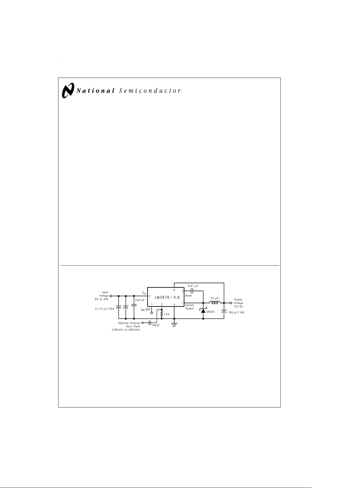
Typical Application
SIMPLE SWITCHER
®
is a registered trademark of National Semiconductor Corporation.
DS100942-3
August 1998
LM2670 SIMPLE SWITCHER High Efficiency 3A Step-Down Voltage Regulator with Sync
© 1999 National Semiconductor Corporation DS100942 www.national.com
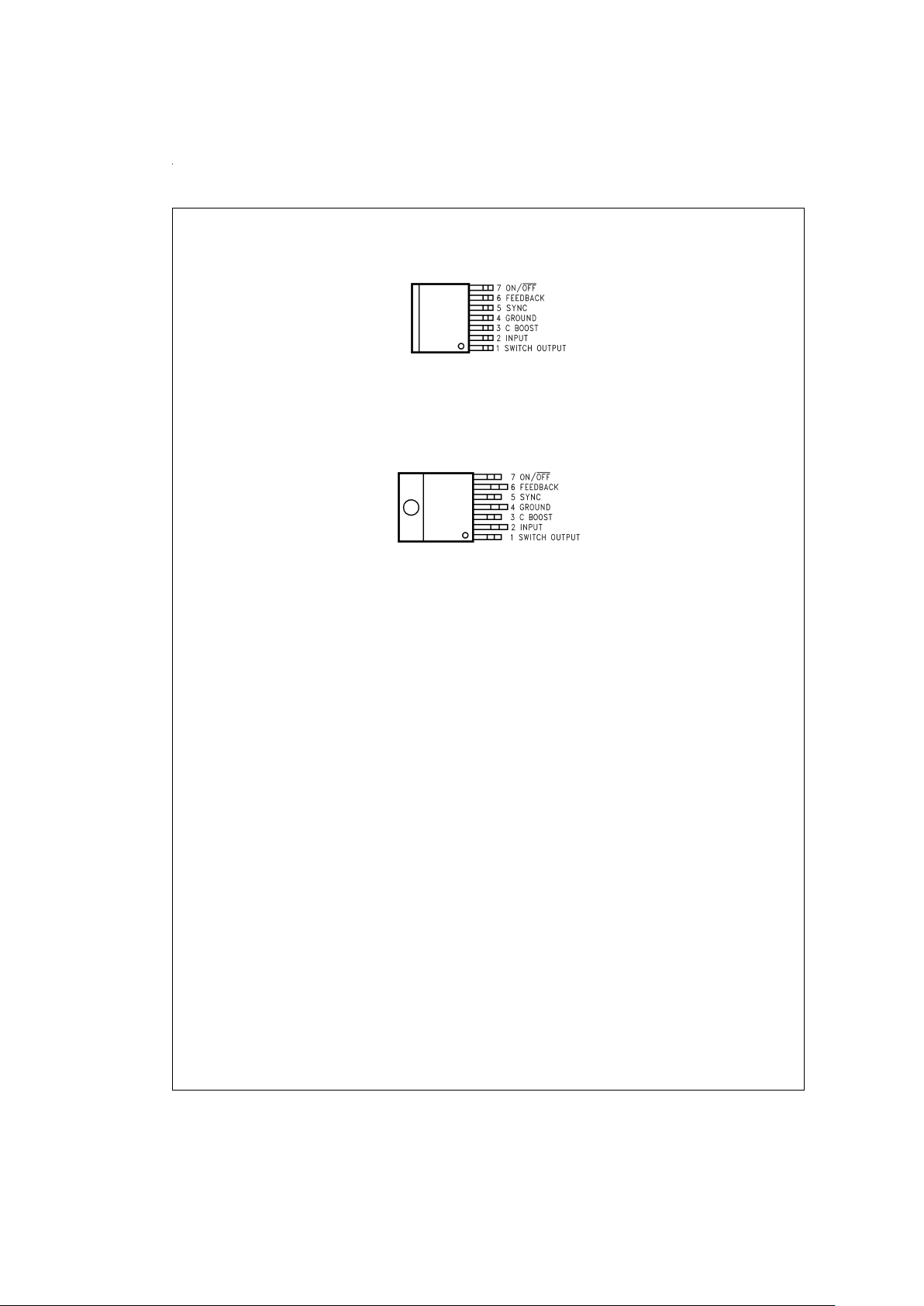
Connection Diagram and Ordering Information
TO-263 Package
Top View
DS100942-1
Order Number
LM2670S-3.3, LM2670S-5.0,
LM2670S-12 or LM2670S-ADJ
See NSC Package Number TS7B
TO-220 Package
Top View
DS100942-2
Order Number
LM2670T-3.3, LM2670T-5.0,
LM2670T-12 or LM2670T-ADJ
See NSC Package Number TA07B
www.national.com 2

Absolute Maximum Ratings (Note 1)
If Military/Aerospace specified devices are required,
please contact the National Semiconductor Sales Office/
Distributors for availability and specifications.
Input Supply Voltage 45V
ON/OFF Pin Voltage −0.1V to 6V
Switch Voltage to Ground −1V to V
IN
Boost Pin Voltage V
SW
+8V
Feedback Pin Voltage −0.3V to 14V
Power Dissipation Internally Limited
ESD (Note 2) 2 kV
Storage Temperature Range −65˚C to 150˚C
Soldering Temperature
Wave 4 sec, 260˚C
Infrared 10 sec, 240˚C
Vapor Phase 75 sec, 219˚C
Operating Ratings
Supply Voltage 8V to 40V
Junction Temperature Range (T
J
) −40˚C to 125˚C
Thermal Resistance (θ
JA
) 30˚C/W
Thermal Resistance (θ
JC
) 2˚C/W
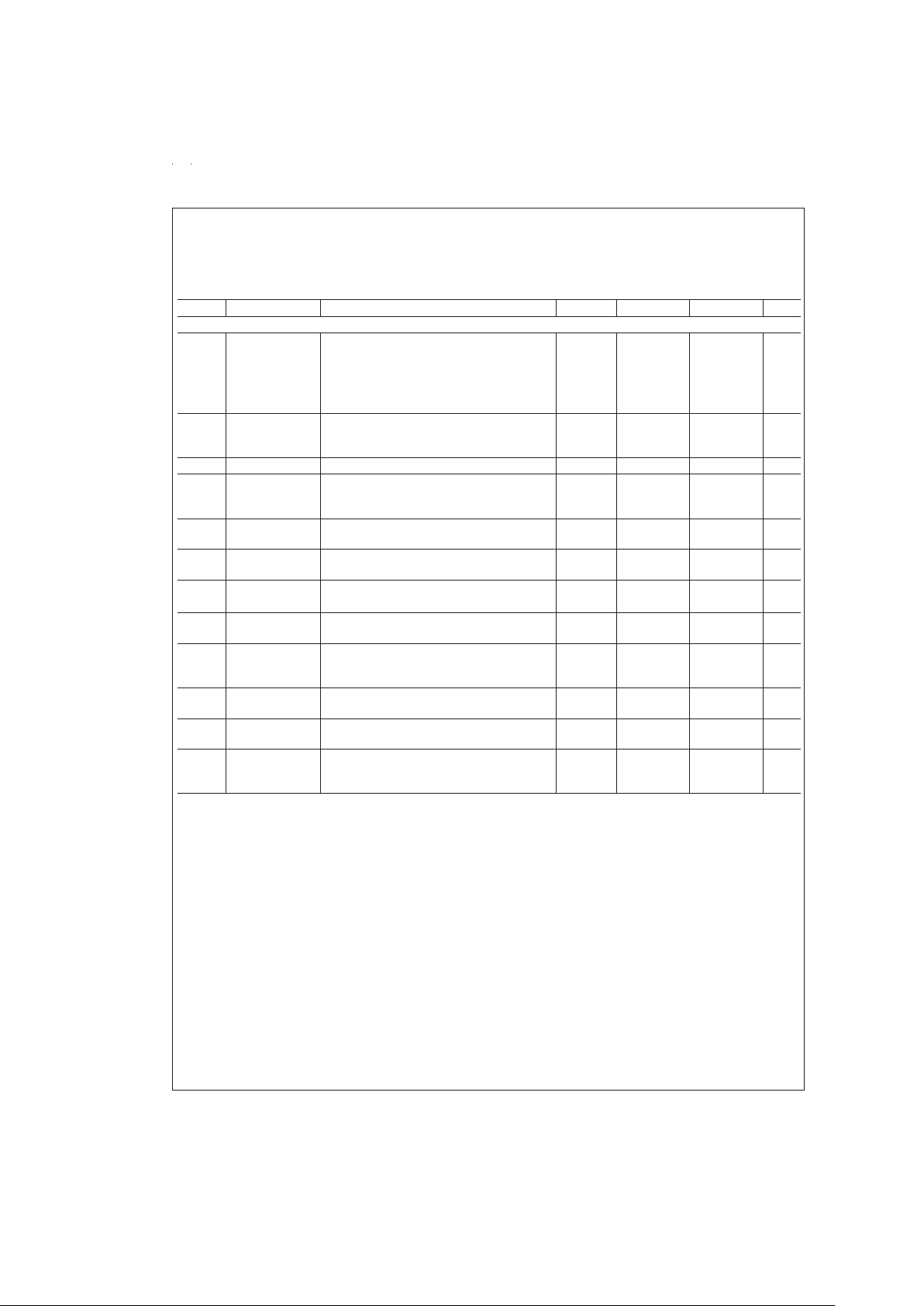
Electrical Characteristics Limits appearing in bold type face apply over the entire junction temperature
range of operation, −40˚C to 125˚C. Specifications appearing in normal type apply for T
A
=
T
J
=
25˚C. Sync pin open cir-
cuited.
LM2670-3.3
Symbol Parameter Conditions Typical Min Max Units
(Note 3) (Note 4) (Note 4)
V
OUT
Output Voltage V
IN
=
8V to 40V, 100mA ≤ I
OUT
≤ 3A 3.3 3.234/3.201 3.366/3.399 V
η Efficiency V
IN
=
12V, I
LOAD
=
3A 86
%
LM2670-5.0
Symbol Parameter Conditions Typical Min Max Units
(Note 3) (Note 4) (Note 4)
V
OUT
Output Voltage V
IN
=
8V to 40V, 100mA ≤ I
OUT
≤ 3A 5.0 4.900/4.850 5.100/5.150 V
η Efficiency V
IN
=
12V, I
LOAD
=
3A 88
%
LM2670-12
Symbol Parameter Conditions Typical Min Max Units
(Note 3) (Note 4) (Note 4)
V
OUT
Output Voltage V
IN
=
15V to 40V, 100mA ≤ I
OUT
≤ 3A 12 11.76/11.64 12.24/12.36 V
η Efficiency V
IN
=
24V, I
LOAD
=
3A 94
%
LM2670-ADJ
Symbol Parameter Conditions Typ Min Max Units
(Note 3) (Note 4) (Note 4)
V
FB
Feedback
Voltage
V
IN
=
8V to 40V, 100mA ≤ I
OUT
≤ 3A
V
OUT
Programmed for 5V
1.21 1.186/1.174 1.234/1.246 V
η Efficiency V
IN
=
12V, I
LOAD
=
3A 88
%
www.national.com3
All Output Voltage Versions
Electrical Characteristics
Limits appearing in bold type face apply over the entire junction temperature range of operation, −40˚C to 125˚C.
Specifications appearing in normal type apply for T
A
=
T
J
=
25˚C. Unless otherwise specified V
IN
=
12V for the 3.3V, 5V and
Adjustable versions and V
IN
=
24V for the 12V version, Sync pin open circuited..
Symbol Parameter Conditions Typ Min Max Units
DEVICE PARAMETERS
I
Q
Quiescent
Current V
FEEDBACK
=
8V 4.2 6 mA
For 3.3V, 5.0V, and ADJ Versions
V
FEEDBACK
=
15V
For 12V Versions
I
STBY
Standby
Quiescent
Current
ON/OFF Pin
=
0V
50 100/150 µA
I
CL
Current Limit 4.5 3.8/3.6 5.25/5.4 A
I
L
Output
Leakage
Current
V
IN
=
40V, ON/OFF Pin
=
0V
V
SWITCH
=
0V
V
SWITCH
=
−1V
16
200
15
µA
mA
R
DS(ON)
Switch
On-Resistance
I
SWITCH
=
3A
0.15 0.17/0.29 Ω
f
O
Oscillator
Frequency
Measured at Switch Pin
260 225 280 kHz
D Duty Cycle Maximum Duty Cycle 91
%
Minimum Duty Cycle 0
%
I
BIAS
Feedback Bias
Current
V
FEEDBACK
=
1.3V
ADJ Version Only
85 nA
V
ON/OFF
ON/OFF
Threshold
Voltage
1.4 0.8 2.0 V
I
ON/OFF
ON/OFF Input
Current
ON/OFF Input
=
0V
20 45 µA
F
SYNC
Synchronization
Frequency
V
SYNC
(Pin 5)
=
3.5V, 50
%
Duty Cycle
400 KHz
V
SYNC
SYNC
Threshold
Voltage
1.4 V
Note 1: Absolute Maximum Ratings are limits beyond which damage to the device may occur. Operating Ratings indicate conditions under which of the device is
guaranteed. Operating Ratings do not imply guaranteed performance limits. For guaranteed performance limits and associated test condition, see the electrical Char-
acteristics tables.
Note 2: ESD was applied using the human-body model, a 100pF capacitor discharged through a 1.5 kΩ resistor into each pin.
Note 3: Typical values are determined with T
A
=
T
J
=
25˚C and represent the most likely norm.
Note 4: All limits are guaranteed at room temperature (standard type face) and at temperature extremes (bold type face). All room temperature limits are 100
%
tested during production with T
A
=
T
J
=
25˚C. All limits at temperature extremes are guaranteed via correlation using standard standard Quality Control (SQC) meth-
ods. All limits are used to calculateAverage Outgoing Quality Level (AOQL).
www.national.com 4
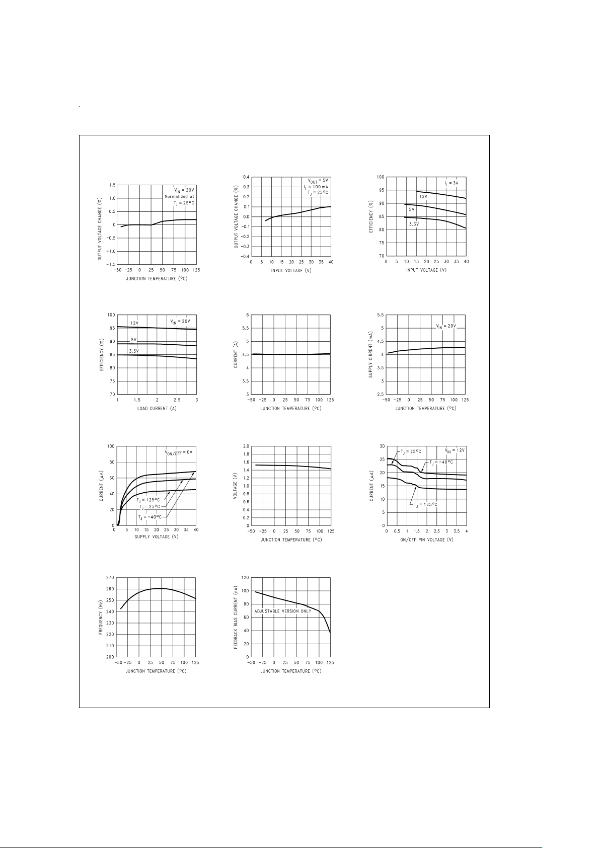
Typical Performance Characteristics
Normalized
Output Voltage
DS100942-9
Line Regulation
DS100942-10
Efficiency vs Input Voltage
DS100942-11
Efficiency vs I
LOAD
DS100942-12
Switch Current Limit
DS100942-4
Operating Quiescent Current
DS100942-5
Standby Quiescent Current
DS100942-40
ON/OFF Threshold Voltage
DS100942-13
ON/OFF Pin Current (Sourcing)
DS100942-14
Switching Frequency
DS100942-15
Feedback Pin Bias Current
DS100942-16
www.national.com5
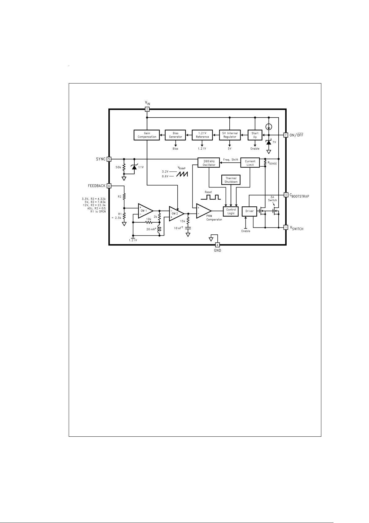
Block Diagram
DS100942-6
* Active Inductor Patent Number 5,514,947
†
Active Capacitor Patent Number 5,382,918
www.national.com 6
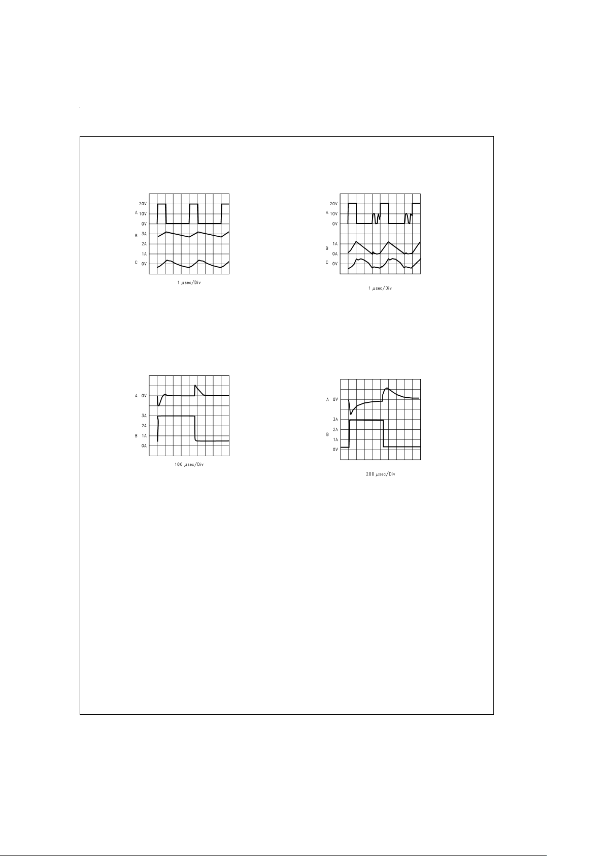
Typical Performance Characteristics
Continuous Mode Switching Waveforms
V
IN
=
20V, V
OUT
=
5V, I
LOAD
=
3A
L
=
33 µH, C
OUT
=
200 µF, C
OUT
ESR
=
26 mΩ
DS100942-17
A: V
SW
Pin Voltage, 10 V/div.
B: Inductor Current, 1 A/div
C: Output Ripple Voltage, 20 mV/div AC-Coupled
Horizontal Time Base: 1 µs/div
Discontinuous Mode Switching Waveforms
V
IN
=
20V, V
OUT
=
5V, I
LOAD
=
500 mA
L
=
10 µH, C
OUT
=
400 µF, C
OUT
ESR
=
13 mΩ
DS100942-18
A: V
SW
Pin Voltage, 10 V/div.
B: Inductor Current, 1 A/div
C: Output Ripple Voltage, 20 mV/div AC-Coupled
Horizontal Time Base: 1 µs//iv
Load Transient Response for Continuous Mode
V
IN
=
20V, V
OUT
=
5V
L
=
33 µH, C
OUT
=
200 µF, C
OUT
ESR
=
26 mΩ
DS100942-19
A: Output Voltage, 100 mV//div, AC-Coupled.
B: Load Current: 500 mA to 3A Load Pulse
Horizontal Time Base: 100 µs/div
Load Transient Response for Discontinuous Mode
V
IN
=
20V, V
OUT
=
5V,
L
=
10 µH, C
OUT
=
400 µF, C
OUT
ESR
=
13 mΩ
DS100942-20
A: Output Voltage, 100 mV/div, AC-Coupled.
B: Load Current: 200 mA to 3A Load Pulse
Horizontal Time Base: 200 µs/div
www.national.com7
 Loading...