


Integrated Device Technology Inc 7429FCT53BTQ, 7429FCT53BTPYB, 7429FCT53BTPY, 7429FCT53BTPB, 7429FCT53BTP Datasheet
...
FAST CMOS |
IDT29FCT52AT/BT/CT/DT |
OCTAL REGISTERED |
IDT29FCT2052AT/BT/CT |
TRANSCEIVERS |
IDT29FCT53AT/BT/CT |
|
Integrated Device Technology, Inc.
FEATURES:
•Common features:
–Low input and output leakage ≤1μA (max.)
–CMOS power levels
–True TTL input and output compatibility
–VOH = 3.3V (typ.)
–VOL = 0.3V (typ.)
–Meets or exceeds JEDEC standard 18 specifications
–Product available in Radiation Tolerant and Radiation Enhanced versions
–Military product compliant to MIL-STD-883, Class B and DESC listed (dual marked)
–Available in DIP, SOIC, SSOP, QSOP, CERPACK and LCC packages
•Features for 29FCT52/29FCT53T:
–A, B, C and D speed grades
–High drive outputs (-15mA IOH, 64mA IOL)
–Power off disable outputs permit “live insertion”
•Features for 29FCT2052T:
–A, B and C speed grades
– |
Resistor outputs (-15mA IOH, 12mA IOL Com.) |
|
(-12mA IOH, 12mA IOL Mil.) |
– |
Reduced system switching noise |
DESCRIPTION:
The IDT29FCT52AT/BT/CT/DT and IDT29FCT53AT/BT/ CT are 8-bit registered transceivers built using an advanced dual metal CMOS technology. Two 8-bit back-to-back registers store data flowing in both directions between two bidirectional buses. Separate clock, clock enable and 3-state output enable signals are provided for each register. Both A outputs and B outputs are guaranteed to sink 64mA.
The IDT29FCT52AT/BT/CT/DT and IDT29FCT2052AT/BT/ CT are non-inverting options of the IDT29FCT53AT/BT/CT.
The IDT29FCT2052AT/BT/CT has balanced drive outputs with current limiting resistors. This offers low ground bounce, minimal undershoot and controlled output fall times-reducing the need for external series terminating resistors. The IDT29FCT2052T part is a plug-in replacement for IDT29FCT52T part.
FUNCTIONAL BLOCK DIAGRAM(1)
CPA |
|
|
|
|
|
CEA |
|
|
|
|
OEB |
|
|
|
|
|
|
A0 |
|
D0 |
CE CP Q0 |
B0 |
|
A1 |
|
D1 |
|
Q1 |
B1 |
A2 |
|
D2 |
|
Q2 |
B2 |
A3 |
|
D3 |
A |
Q3 |
B3 |
A4 |
|
D4 |
Reg. Q4 |
B4 |
|
A5 |
|
D5 |
|
Q5 |
B5 |
A6 |
|
D6 |
|
Q6 |
B6 |
A7 |
|
D7 |
|
Q7 |
B7 |
|
|
|
|
|
|
|
|
|
|
|
|
|
|
Q0 |
|
D0 |
|
|
|
Q1 |
|
D1 |
|
|
|
Q2 |
|
D2 |
|
|
|
Q3 |
B |
D3 |
|
|
|
Q4 Reg. D4 |
|
||
|
|
Q5 |
|
D5 |
|
|
|
Q6 |
|
D6 |
|
|
|
Q7 |
CE CP D7 |
|
|
OEA |
|
|
|
|
CPB |
|
|
|
|
||
NOTE: |
|
|
|
|
|
|
|
|
|
CEB |
|
1. IDT29FCT52T/IDT29FCT2052T function is shown. IDT29FCT53T is |
|
|
|
|
|
the inverting option. |
|
|
|
|
|
The IDT logo is a registered trademark of Integrated Device Technology, Inc. |
|
|
|
|
2629 drw 01 |
|
|
|
|
|
|
|
|
|
|
|
|
MILITARY AND COMMERCIAL TEMPERATURE RANGES |
|
|
JUNE 1995 |
||
|
|
|
|
|
|
©1995 Integrated Device Technology, Inc. |
6.1 |
|
|
DSC-4224/5 |
|
|
|
|
|
|
1 |
IDT29FCT52AT/BT/CT/DT, IDT29FCT/2052AT/BT/CT, IDT29FCT53AT/BT/CT |
|
FAST CMOS OCTAL REGISTERED TRANSCEIVERS |
MILITARY AND COMMERCIAL TEMPERATURE RANGES |
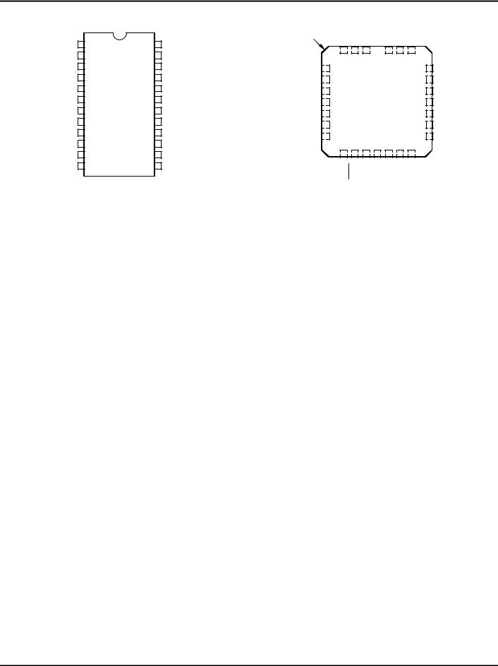
PIN CONFIGURATIONS
B 7 |
1 |
|
24 |
Vcc |
|
B 6 |
2 |
|
23 |
A 7 |
|
B 5 |
3 |
P24-1 |
22 |
A 6 |
|
B 4 |
4 |
21 |
A 5 |
||
B 3 |
5 |
D24-1 |
20 |
A 4 |
|
SO24-2 |
|||||
B 2 |
6 |
19 |
A 3 |
||
|
|
SO24-7* |
|
A 2 |
|
B 1 |
7 |
SO24-8* 18 |
|||
B 0 |
8 |
& |
17 |
A 1 |
|
OEB |
9 |
E24-1 |
16 |
A 0 |
|
|
|||||
CPA |
10 |
|
15 |
OEA |
|
CEA |
11 |
|
14 |
CPB |
|
GND |
12 |
|
13 |
CEB |
|
|
|
|
|
2629 drw 02 |
|
DIP/SOIC/SSOP/QSOP/CERPACK
TOP VIEW
* For 29FCT52/29FCT2052AT/BT/CT only
INDEX
B 4
B 3
B 2
NC
B 1
B 0
OEB
B 5 |
B 6 |
B 7 |
|
NC Vcc A 7 |
A 6 |
|
4 |
3 |
2 |
|
28 27 26 |
||
|
|
|||||
5 |
|
|
|
|
|
25 |
|
|
1 |
|
|||
|
|
|
|
|
||
6 |
|
|
|
|
|
24 |
7 |
|
|
|
|
|
23 |
8 |
|
L28-1 |
22 |
|||
9 |
|
|
|
|
|
21 |
10 |
|
|
|
|
|
20 |
11 |
|
|
|
|
|
19 |
12 13 14 15 16 17 18 |
||||||
CPA |
CEA |
GND |
NC CEB CPB |
OEA |
||
LCC
TOP VIEW
A 5
A 4
A 3
NC
A 2
A 1
A 0
2629 drw 03
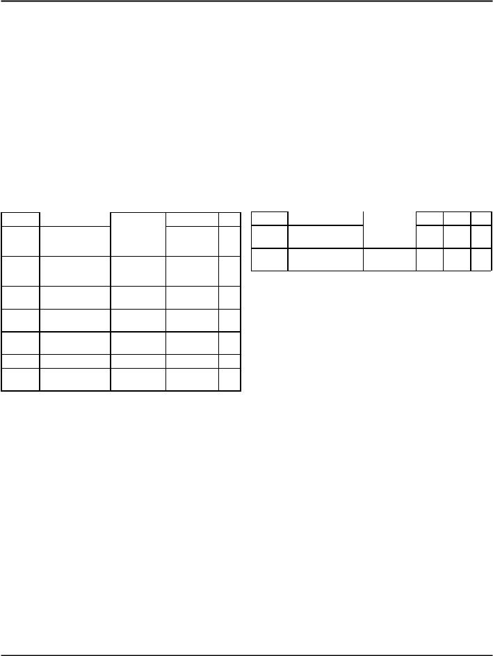
PIN DESCRIPTION
Name |
I/O |
Description |
|
|
|
A0-7 |
I/O |
Eight bidirectional lines carrying the A Register inputs or B Register outputs. |
|
|
|
B0-7 |
I/O |
Eight bidirectional lines carrying the B Register inputs or A Register outputs. |
|
|
|
CPA |
I |
Clock for the A Register. When CEA is LOW, data is entered into the A Register on the LOW-to-HIGH transition of |
|
|
the CPA signal. |
|
|
|
CEA |
I |
Clock Enable for the A Register. When CEA is LOW, data is entered into the A Register on the LOW-to-HIGH transition |
|
|
of the CPA signal. When CEA is HIGH, the A Register holds its contents, regardless of CPA signal transitions. |
|
|
|
OEB |
I |
Output Enable for the A Register. When OEB is LOW, the A Register outputs are enabled onto the B0-7 lines. When |
|
|
OEB is HIGH, the B0-7 outputs are in the high-impedance state. |
|
|
|
CPB |
I |
Clock for the B Register. When CEB is LOW, data is entered into the B Register on the LOW-to-HIGH transition of |
|
|
the CPB signal. |
|
|
|
CEB |
I |
Clock Enable for the B Register. When CEB is LOW, data is entered into the B Register on the LOW-to-HIGH transition |
|
|
of the CPB signal. When CEB is HIGH, the B Register holds its contents, regardless of CPB signal transitions. |
|
|
|
OEA |
I |
Output Enable for the B Register. When OEA is LOW, the B Register outputs are enabled onto the A0-7 lines. When |
|
|
OEA is HIGH, the A0-7 outputs are in the high-impedance state. |
|
|
|
|
|
2629 tbl 01 |
6.1 |
2 |
IDT29FCT52AT/BT/CT/DT, IDT29FCT/2052AT/BT/CT, IDT29FCT53AT/BT/CT |
|
FAST CMOS OCTAL REGISTERED TRANSCEIVERS |
MILITARY AND COMMERCIAL TEMPERATURE RANGES |
REGISTER FUNCTION TABLE(1)
(Applies to A or B Register)
|
Inputs |
|
Internal |
|
D |
CP |
CE |
Q |
Function |
|
|
|
|
|
X |
X |
H |
NC |
Hold Data |
|
|
|
|
|
L |
− |
L |
L |
Load Data |
H |
− |
L |
H |
|
|
|
|
|
|
NOTE: |
2629 tbl 02 |
|
1.H = HIGH Voltage Level L = LOW Voltage Level X = Don’t Care
NC = No Change
− = LOW-to-HIGH Transition
ABSOLUTE MAXIMUM RATINGS(1)
Symbol |
Rating |
Commercial |
Military |
Unit |
VTERM(2) |
Terminal Voltage |
–0.5 to +7.0 |
–0.5 to +7.0 |
V |
|
with Respect to |
|
|
|
|
GND |
|
|
|
VTERM(3) |
Terminal Voltage |
–0.5 to |
–0.5 to |
V |
|
with Respect to |
VCC +0.5 |
VCC +0.5 |
|
|
GND |
|
|
|
TA |
Operating |
0 to +70 |
–55 to +125 |
°C |
|
Temperature |
|
|
|
TBIAS |
Temperature |
–55 to +125 |
–65 to +135 |
°C |
|
Under Bias |
|
|
|
TSTG |
Storage |
–55 to +125 |
–65 to +150 |
°C |
|
Temperature |
|
|
|
PT |
Power Dissipation |
0.5 |
0.5 |
W |
IOUT |
DC Output |
–60 to +120 |
–60 to +120 |
mA |
|
Current |
|
|
|
NOTES: |
2529 lnk 04 |
|
1.Stresses greater than those listed under ABSOLUTE MAXIMUM RATINGS may cause permanent damage to the device. This is a stress rating only and functional operation of the device at these or any other conditions above those indicated in the operational sections of this specification is not implied. Exposure to absolute maximum rating conditions for extended periods may affect reliability. No terminal voltage may exceed VCC by +0.5V unless otherwise noted.
2.Input and VCC terminals only.
3.Outputs and I/O terminals only.
OUTPUT CONTROL(1)
|
Internal |
Y-Outputs |
|
|
|
|
|
|
|
OE |
Q |
52/2052 |
53 |
Function |
|
|
|
|
|
H |
X |
Z |
Z |
Disable Outputs |
|
|
|
|
|
L |
L |
L |
H |
Enable Outputs |
L |
H |
H |
L |
|
|
|
|
|
|
NOTE: |
|
|
|
2629 tbl 03 |
1.H = HIGH Voltage Level L = LOW Voltage Level X = Don’t Care
Z = High Impedance
CAPACITANCE (TA = +25°C, f = 1.0MHz)
Symbol |
Parameter(1) |
Conditions |
Typ. |
Max. |
Unit |
CIN |
Input |
VIN = 0V |
6 |
10 |
pF |
|
Capacitance |
|
|
|
|
COUT |
Output |
VOUT = 0V |
8 |
12 |
pF |
|
Capacitance |
|
|
|
|
NOTE: |
|
|
|
2640 lnk 05 |
|
1. This parameter is measured at characterization but not tested.
6.1 |
3 |
 Loading...