


S886T

S886T/S886TR
Vishay Telefunken
MOSMIC for TV–Tuner Prestage with 12 V Supply
Voltage
MOSMIC - MOS Monolithic Integrated Circuit Electrostatic sensitive device.
Observe precautions for handling.
Applications
Low noise gain controlled input stages in UHF-and
VHF- tuner with 12 V supply voltage.
Features
D
Integrated gate protection diodes
D
Low noise figure
D
High gain
D
Biasing network on chip
21
94 9279
43
S886T Marking: 982
Plastic case (SOT 143)
1 = Source, 2 = Drain, 3 = Gate 2, 4 = Gate 1
13 579
D
RFC
C block
V
DD
RF out
94 9296
C block
AGC
RF in
C block
D
Improved cross modulation at gain reduction
D
High AGC-range
D
SMD package
G2
G1
S
21
94 9278
95 10831
43
S886TR Marking: 82R
Plastic case (SOT 143R)
1 = Source, 2 = Drain, 3 = Gate 2, 4 = Gate 1
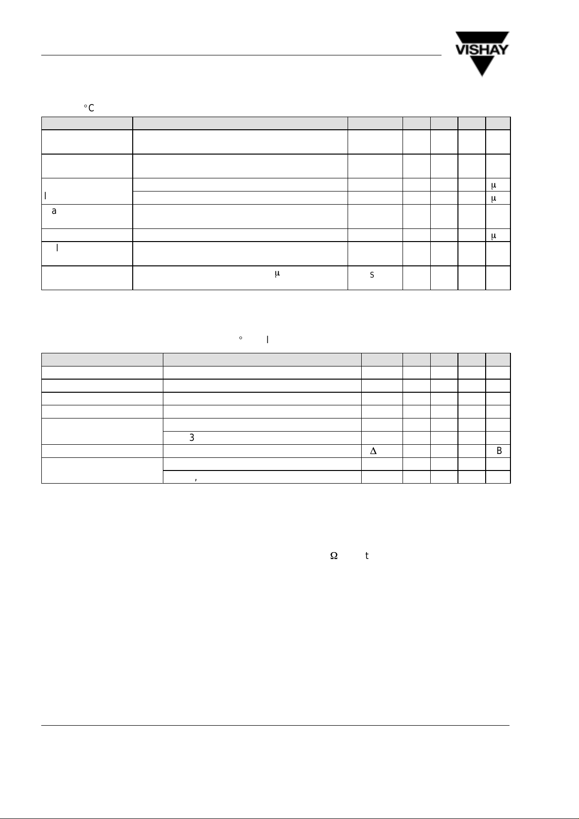
Absolute Maximum Ratings
T
= 25_C, unless otherwise specified
amb
Parameter Test Conditions Symbol Value Unit
Drain - source voltage V
Drain current I
Gate 1/Gate 2 - source peak current ±I
Gate 1/Gate 2 - source voltage ±V
Total power dissipation T
≤ 60 °C P
amb
G1/G2SM
G1/G2SM
Channel temperature T
Storage temperature range T
DS
D
tot
Ch
stg
16 V
30 mA
10 mA
7.5 V
200 mW
150
–55 to +150
Maximum Thermal Resistance
T
= 25_C, unless otherwise specified
amb
Parameter T est Conditions Symbol Value Unit
Channel ambient on glass fibre printed board (25 x 20 x 1.5) mm
plated with 35mm Cu
Document Number 85057
Rev. 3, 20-Jan-99
3
R
thChA
www.vishay.de • FaxBack +1-408-970-5600
450 K/W
°
°
C
C
1 (8)
S886T/S886TR
g
g
Vishay Telefunken
Electrical DC Characteristics
T
= 25_C, unless otherwise specified
amb
Parameter Test Conditions Symbol Min Typ Max Unit
Gate 1 - source
breakdown voltage
Gate 2 - source
breakdown voltage
Gate 1 - source +V
leakage current
Gate 2 - source
leakage current
Drain current VDS = 12 V, V
Self-biased
operating current
Gate 2 - source
cut-off voltage
Electrical AC Characteristics
±I
= 10 mA, V
G1S
±I
= 10 mA, V
G2S
= 6 V, V
G1S
–V
= 6 V, V
G1S
±V
= 6 V, V
G2S
VDS = 12 V, V
VDS = 12 V, V
= VDS = 0 ±V
G2S
= VDS = 0 ±V
G1S
= VDS = 0 +I
G2S
= VDS = 0 –I
G2S
= VDS = 0 ±I
G1S
= 0, V
G1S
= nc, V
G1S
= nc, ID = 200 mA V
G1S
= 6 V I
G2S
= 6 V I
G2S
(BR)G1SS
(BR)G2SS
G1SS
G1SS
G2SS
DSS
DSP
G2S(OFF)
8 12 V
8 12 V
50 500mA
8 12 16 mA
1.0 V
60
m
120mA
20 nA
A
VDS = 12 V, V
= 6 V, f = 1 MHz , T
G2S
= 25_C, unless otherwise specified
amb
Parameter Test Conditions Symbol Min Typ Max Unit
Forward transadmittance y
Gate 1 input capacitance C
Feedback capacitance C
Output capacitance C
Power gain GS = 2 mS, GL = 0.5 mS, f = 200 MHz G
GS = 3,3 mS, GL = 1 mS, f = 800 MHz G
AGC range VDS = 12 V, V
= 1 to 6 V, f = 800 MHz
G2S
25 30 35 mS
21s
2.3 2.7 pF
20 fF
0.9 pF
27 dB
45 dB
D
issg1
rss
oss
ps
ps
G
ps
17.5 22 dB
Noise figure GS = 2 mS, GL = 0.5 mS, f = 200 MHz F 1 dB
GS = 3,3 mS, GL = 1 mS, f = 800 MHz F 1.3 dB
Caution for Gate 1 switch-off mode:
No external DC-voltage on Gate 1 in active mode!
Switch-off at Gate 1 with V
Using open collector switching transistor (inside of PLL), insert 10 kW collector resistor.
< 0.7 V is feasible.
G1S
www.vishay.de • FaxBack +1-408-970-5600
2 (8)
Document Number 85057
Rev. 3, 20-Jan-99
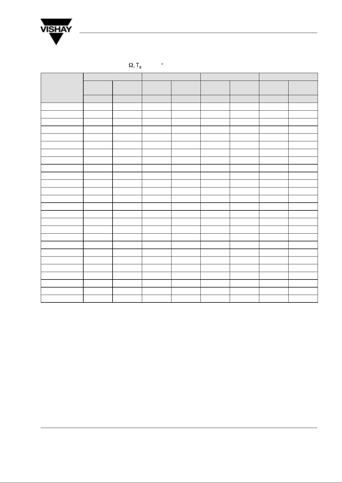
Common Source S–Parameters
S886T/S886TR
Vishay Telefunken
VDS = 12 V , V
f/MHz
50 –0.02 –4.8 10.29 174.4 –61.79 87.6 –0.35 –1.9
100 –0.05 –9.3 10.20 168.1 –55.74 84.8 –0.38 –3.7
150 –0.14 –13.8 10.10 161.6 –52.32 81.5 –0.40 –5.5
200 –0.23 –18.2 9.97 155.4 –50.05 79.2 –0.43 –7.3
250 –0.35 –22.5 9.78 148.7 –48.45 76.3 –0.45 –9.1
300 –0.48 –26.6 9.64 143.2 –47.20 74.5 –0.47 –10.5
350 –0.63 –30.8 9.40 137.5 –46.23 72.5 –0.51 –12.2
400 –0.80 –34.7 9.24 132.0 –45.57 71.2 –0.55 –13.8
450 –0.95 –38.4 8.95 126.1 –45.19 69.4 –0.60 –15.3
500 –1.15 –42.2 8.74 121.1 –44.92 68.7 –0.63 –17.1
550 –1.31 –45.7 8.54 116.4 –44.76 69.0 –0.67 –18.4
600 –1.46 –49.3 8.31 111.2 –44.58 70.8 –0.69 –19.9
650 –1.62 ––52.4 8.07 106.6 –44.57 72.3 –0.72 –21.6
700 –1.81 –56.0 7.85 101.9 –44.75 73.4 –0.75 –22.7
750 –1.95 –58.9 7.67 97.3 –45.03 76.3 –0.77 –24.6
800 –2.11 –62.0 7.47 92.7 –45.27 81.0 –0.79 –25.8
850 –2.26 –65.3 7.28 87.8 –45.52 86.6 –0.81 –27.5
900 –2.37 –68.2 7.08 83.3 –45.41 94.9 –0.83 –29.1
950 –2.49 –71.5 6.94 79.3 –44.79 103.7 –0.85 –31.0
1000 –2.62 –74.5 6.71 74.6 –44.21 107.4 –0.87 –32.3
1050 –2.76 –77.5 6.62 70.9 –43.95 113.3 –0.89 –33.9
1100 –2.90 –80.2 6.44 66.0 –43.64 120.8 –0.90 –35.3
1150 –2.98 –83.2 6.34 62.2 –42.73 128.9 –0.87 –37.2
1200 –3.07 –86.0 6.17 57.3 –41.82 135.7 –0.85 –38.8
1250 –3.14 –88.8 6.11 53.6 –40.68 142.1 –0.80 –40.4
1300 –3.24 –91.6 6.00 48.8 –39.80 146.1 –0.76 –42.4
= 6 V , Z0 = 50 W,T
G2S
S11 S21 S12 S22
LOG
MAG
dB deg dB deg dB deg dB deg
ANG
= 25_C, unless otherwise specified
amb
LOG
MAG
ANG
LOG
MAG
ANG
LOG
MAG
ANG
Document Number 85057
Rev. 3, 20-Jan-99
www.vishay.de • FaxBack +1-408-970-5600
3 (8)
 Loading...