


TFDS6402
TFDU6102E/TFDS6402/TFDS6502E/TFDT6502E
Vishay Semiconductor
Fast Infrared Transceiver Module Family (FIR, 4 Mbit/s) for 2.6 V to 5.5 V Operation
Description
The TFDU6102E, TFDS6402, TFDS6502E, TFDT6502E are a family of low±power infrared transceiver modules compliant to the IrDA physical layer standard for fast infrared data communication, supporting IrDA speeds up to 4.0 Mbit/s (FIR), HP-SIR, Sharp ASK and carrier based remote control modes up to 2 MHz. Integrated within the transceiver modules are a photo PIN diode, an infrared emitter (IRED), and a low±power CMOS control IC to provide a total front±end solution in a single package.
Vishay Telefunken's FIR transceivers are available in four package options, including our Baby Face package (TFDU610xE), the standard setting, once
smallest FIR transceiver available on the market. This wide selection provides flexibility for a variety of applications and space constraints. The transceivers are capable of directly interfacing with a wide variety of I/O devices which perform the modulation/ demodulation function, including National Semiconductor's PC87338, PC87108 and PC87109, SMC's FDC37C669, FDC37N769 and CAM35C44, and Hitachi's SH3. At a minimum, a current±limiting resistor in series with the infrared emitter and a VCC bypass capacitor are the only external components required implementing a complete solution.
Features
Compliant to the IrDA physical layer specification
(Up to 4 Mbit/s),
HP±SIR , Sharp ASK and TV Remote Control
For 3.0 V and 5.0 V Applications
Operates from 2.6 V to 5.5 V within specification, operational down to 2.4 V
Low Power Consumption (3 mA Supply Current)
Power Shutdown Mode (1 A Shutdown Current)
Four Surface Mount Package Options
±Universal (9.7 × 4.7 × 4.0 mm)
±Side View (13.0 × 5.95 × 5.3 mm)
±Top View (13.0 × 7.6 × 5.95 mm)
±Dracula (11.2 × 5.6 × 2.2 mm)
Push-Pull-Receiver Output, grounded in shutdown mode
High Efficiency Emitter
Baby Face (Universal) Package Capable of Surface Mount Soldering to Side and Top View Orientation
Directly Interfaces with Various Super I/O and Controller Devices
Built±In EMI Protection ± No External Shielding Necessary
Few External Components Required
Backward Pin to Pin Compatible to all Vishay Telefunken SIR and FIR Infrared Transceivers
Split power supply, transmitter and receiver can be operated from two power supplies with relaxed requirements, thus saving costs
Applications
Notebook Computers, Desktop PCs, |
Telecommunication Products |
Palmtop Computers (Win CE, Palm PC), PDAs |
(Cellular Phones, Pagers) |
Digital Still and Video Cameras |
Internet TV Boxes, Video Conferencing Systems |
Printers, Fax Machines, Photocopiers, |
External Infrared Adapters (Dongles) |
|
|
Screen Projectors |
Medical and Industrial Data Collection Devices |
Document Number 82526 |
www.vishay.com |
Rev. B1.6, 02±Nov±00 |
1 |

TFDU6102E/TFDS6402/TFDS6502E/TFDT6502E
Vishay Semiconductor
Package Options
TFDU6102E |
TFDS6402 |
TFDS6502E |
TFDT6502E |
Baby Face (Universal) |
Dracula Side View |
Side View |
Top View |
weight 0.20 g |
weight 0.30 g |
weight 0.39 g |
weight 0.39 g |
Ordering Information
Part Number |
Qty / Reel |
Description |
TFDU6102E±TR3 |
1000 pcs |
Oriented in carrier tape for side view surface mounting |
TFDU6102E±TT3 |
1000 pcs |
Oriented in carrier tape for top view surface mounting |
TFDS6402±TR3 |
1000 pcs |
Side View |
TFDS6502E±TR3 |
750 pcs |
Side View |
TFDT6502E±TR3 |
750 pcs |
Top View |
Functional Block Diagram
VCC
|
|
|
Driver |
|
Amplifier |
Comparator |
Rxd |
|
AGC |
|
IRED Anode |
SD/Mode |
|
|
|
Logic |
|
|
|
|
|
|
|
Txd |
Open Drain Driver |
IRED Cathode |
|
|
|
||
|
|
GND |
|
Figure 1. Functional Block Diagram
www.vishay.com |
Document Number 82526 |
2 |
Rev. B1.6, 02±Nov±00 |
TFDU6102E/TFDS6402/TFDS6502E/TFDT6502E
Vishay Semiconductor
Pin Description
Pin Number |
|
Function |
Description |
I/O |
Active |
|
ªUº and ªTº Optio |
nªSº Option |
|
|
|
|
|
1 |
|
8 |
IRED Anode |
IRED anode, to be externally connected |
|
|
|
|
|
|
to VCC through a current control resistor. |
|
|
|
|
|
|
This pin is allowed to be supplied from |
|
|
|
|
|
|
an uncontrolled power supply separated |
|
|
|
|
|
|
from the controlled VCC supply |
|
|
2 |
|
1 |
IRED Cathode |
IRED cathode, internally connected to |
|
|
|
|
|
|
driver transistor |
|
|
3 |
|
7 |
Txd |
Transmit Data Input |
I |
HIGH |
4 |
|
2 |
Rxd |
Received Data Output, push-pull CMOS |
O |
LOW |
|
|
|
|
driver output capable of driving a stan- |
|
|
|
|
|
|
dard CMOS or TTL load. No external |
|
|
|
|
|
|
pull-up or pull-down resistor is required. |
|
|
|
|
|
|
Pin is floating when |
|
|
|
|
|
|
device is in shutdown mode |
|
|
5 |
|
6 |
SD/Mode |
Shutdown/ Mode |
I |
HIGH |
6 |
|
3 |
VCC |
Supply Voltage |
|
|
7 |
|
5 |
Mode |
HIGH: High speed mode; |
I |
|
|
|
|
|
LOW: Low speed mode, SIR only |
|
|
|
|
|
|
(see chapter ªMode Switchingº) |
|
|
8 |
|
4 |
GND |
Ground |
|
|
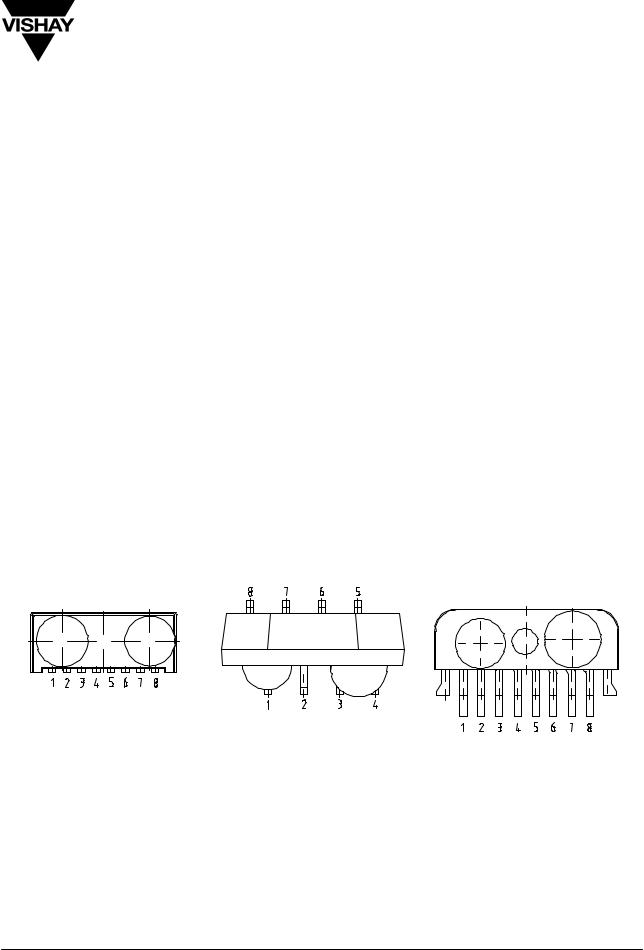
ªUº Option Baby Face (Universal) |
ªSº Option Side View |
ªTº Option Top View |
||
|
and Dracula |
|
|
|
IRED |
Detector |
|
IRED |
Detector |
14885 |
IRED |
Detector |
Figure 2. Pinnings
Document Number 82526 |
www.vishay.com |
Rev. B1.6, 02±Nov±00 |
3 |

TFDU6102E/TFDS6402/TFDS6502E/TFDT6502E
Vishay Semiconductor
Absolute Maximum Ratings
Reference point Pin: GND unless otherwise noted.
Typical values are for DESIGN AID ONLY, not guaranteed nor subject to production testing.
Parameters |
Test Conditions |
Symbol |
Min. |
Typ. |
Max. |
Unit |
Supply Voltage Range, |
0 V <VCC2 <6 V |
VCC1 |
± 0.5 |
|
6 |
V |
Transceiver |
|
|
|
|
|
|
Supply Voltage Range, |
0 V <VCC1 <6 V |
VCC2 |
± 0.5 |
|
6 |
V |
Transmitter |
|
|
|
|
|
|
Input Currents |
For all Pins, Except IRED |
|
|
|
10 |
mA |
|
Anode Pin |
|
|
|
|
|
Output Sinking Current |
|
|
|
|
25 |
mA |
Power Dissipation |
See Derating Curve |
PD |
|
|
350 |
mW |
Junction Temperature |
|
TJ |
|
|
125 |
°C |
Ambient Temperature |
|
Tamb |
±25 |
|
+85 |
°C |
Range (Operating) |
|
|
|
|
|
|
Storage Temperature |
|
Tstg |
±25 |
|
+85 |
°C |
Range |
|
|
|
|
|
|
Soldering Temperature |
See Recommended Solder |
|
|
|
240 |
°C |
|
Profile (see Figure 11) |
|
|
|
|
|
Average Output Current |
|
IIRED (DC) |
|
|
130 |
mA |
Repetitive Pulsed Output |
<90 μs, ton <20% |
IIRED (RP) |
|
|
600 |
mA |
Current |
|
|
|
|
|
|
IRED Anode Voltage |
|
VIREDA |
± 0.5 |
|
6 |
V |
Transmitter Data Input |
|
VTxd |
± 0.5 |
|
VCC1 +0.5 |
V |
Voltage |
|
|
|
|
|
|
Receiver Data Output |
|
VRxd |
± 0.5 |
|
VCC1 +0.5 |
V |
Voltage |
|
|
|
|
|
|
Virtual Source Size |
Method: |
d |
2.5 |
2.8 |
|
mm |
|
(1±1/e) encircled energy |
|
|
|
|
|
Maximum Intensity for |
EN60825, 1997, |
|
|
|
320 |
mW/sr |
Class 1 Operation of |
unidirectional operation, |
|
|
|
|
|
IEC825±1 or EN60825±1 |
worst case test mode |
|
|
|
|
|
(worst case IrDA FIR |
|
|
|
|
|
|
pulse pattern) |
|
|
|
|
|
|
www.vishay.com |
Document Number 82526 |
4 |
Rev. B1.6, 02±Nov±00 |

TFDU6102E/TFDS6402/TFDS6502E/TFDT6502E
Vishay Semiconductor
Electrical Characteristics
Tamb = 25_C, VCC = 2.6V to 5.5 V unless otherwise noted.
Typical values are for DESIGN AID ONLY, not guaranteed nor subject to production testing.
|
Parameters |
Test Conditions / Pins |
Symbol |
Min. |
Typ. |
Max. |
|
Unit |
Transceiver |
|
|
|
|
|
|
|
|
Supply Voltage |
|
VCC |
2.6 |
|
5.5 |
|
V |
|
Dynamic Supply Current |
Receive mode only. |
|
|
|
|
|
|
|
|
|
In transmit mode, add additional 85 mA (typ) for IRED current |
|
|||||
|
|
SD = Low, Ee = 0 klx |
ICC |
|
3 |
4.5 |
|
mA |
|
|
SD = Low, Ee = 1 klx *) |
ICC |
|
3 |
4.5 |
|
mA |
Standby Supply Current |
SD = High, |
ISD |
|
|
|
|
|
|
|
|
Mode = Floating, |
|
|
|
|
|
|
|
|
T = 25°C, Ee = 0 klx |
|
|
|
1 |
|
μA |
|
|
T = 25°C, Ee = 1 klx *) |
|
|
|
1.5 |
|
μA |
|
|
SD = High, T = 85°C, |
ISD |
|
|
5 |
|
μA |
|
|
Mode = Floating, |
|
|
|
|
|
|
|
|
Not Ambient Light |
|
|
|
|
|
|
|
|
Sensitive |
|
|
|
|
|
|
Operating Temperature |
|
TA |
±25 |
|
+85 |
|
°C |
|
Range |
|
|
|
|
|
|
|
|
Output Voltage Low |
Rload = 2.2 kW, |
VOL |
|
0.5 |
0.8 |
|
V |
|
|
|
Cload = 15 pF |
|
|
|
|
|
|
Output Voltage High |
Rload = 2.2 kW, |
VOH |
VCC±0.5 |
|
|
|
V |
|
|
|
Cload = 15 pF |
|
|
|
|
|
|
Input Voltage Low |
|
VIL |
0 |
|
0.8 |
|
V |
|
(Txd, SD/ Mode, Mode) |
|
|
|
|
|
|
|
|
Input Voltage High |
CMOS level **) |
VIH |
0.9 x VCC |
|
|
|
V |
|
(Txd, SD/ Mode, Mode) |
TTL level, VCC ≥ 4.5 V |
VIH |
2.4 |
|
|
|
V |
|
Input Leakage Current |
|
IL |
±10 |
|
+10 |
|
μA |
|
(Txd, SD/ Mode) |
|
|
|
|
|
|
|
|
Input Leakage Current, |
|
IL |
±80 |
|
+80 |
|
μA |
|
Mode |
|
|
|
|
|
|
|
|
Input Capacitance |
|
CI |
|
|
5 |
|
pF |
|
*) |
Standard Illuminant A |
|
|
|
|
|
|
|
**) |
The typical threshold level is between 0.5 x VCC/2 (VCC = 3 V) and 0.4 x VCC (VCC = 5.5 V) . |
|
||||||
|
It is recommended to use the specified min/ max values to avoid increased operating current. |
|
||||||
Document Number 82526 |
www.vishay.com |
Rev. B1.6, 02±Nov±00 |
5 |

TFDU6102E/TFDS6402/TFDS6502E/TFDT6502E
Vishay Semiconductor
Optoelectronic Characteristics
Tamb = 25_C, VCC = 2.6 V to 5.5 V unless otherwise noted.
Typical values are for DESIGN AID ONLY, not guaranteed nor subject to production testing.
Parameters |
Test Conditions |
Symbol |
Min. |
Typ. |
Max. |
Unit |
Receiver |
|
|
|
|
|
|
Minimum Detection |
TFDS6502E/ TFDT6502E |
Ee |
|
20 |
35 |
mW/m2 |
Threshold Irradiance, |
9.6 kbit/s to 115.2 kbit/s |
|
|
|
|
|
SIR Mode |
l = 850 nm to 900 nm |
|
|
|
|
|
|
TFDU6102E, TFDS6402 |
Ee |
|
25 |
40 |
mW/m2 |
|
9.6 kbit/s to 115.2 kbit/s |
|
|
|
|
|
|
l = 850 nm to 900 nm |
|
|
|
|
|
Minimum Detection |
TFDS6502E/ TFDT6502E |
Ee |
|
50 |
|
mW/m2 |
Threshold Irradiance, |
1.152 Mbit/s |
|
|
|
|
|
MIR Mode |
l = 850 nm to 900 nm |
|
|
|
|
|
|
TFDU6102E, TFDS6402 |
Ee |
|
65 |
|
mW/m2 |
|
1.152 Mbit/s |
|
|
|
|
|
|
l = 850 nm to 900 nm |
|
|
|
|
|
Minimum Detection |
TFDS6502E/ TFDT6502E |
Ee |
|
65 |
100 |
mW/m2 |
Threshold Irradiance, |
4.0 Mbit/s |
|
|
|
|
|
FIR Mode |
l = 850 nm to 900 nm |
|
|
|
|
|
|
TFDU6102E, TFDS6402 |
Ee |
|
85 |
100 |
mW/m2 |
|
4.0 Mbit/s |
|
|
|
|
|
|
l = 850 nm to 900 nm |
|
|
|
|
|
Maximum Detection |
l = 850 nm to 900 nm |
Ee |
5 |
10 |
|
kW/m2 |
Threshold Irradiance |
|
|
|
|
|
|
Logic LOW Receiver |
|
Ee |
4 |
|
|
mW/m2 |
Input Irradiance |
|
|
|
|
|
|
Rise Time of Output |
10% to 90%, @2.2 kΩ, 15 pF |
tr (Rxd) |
10 |
|
40 |
ns |
Signal±±,,,,klll |
|
|
|
|
|
|
Fall Time of Output |
90% to 10%, @2.2 kΩ, 15 pF |
tf (Rxd) |
10 |
|
40 |
ns |
Signal |
|
|
|
|
|
|
Rxd Pulse Width of |
Input pulse length 20 μs, 9.6 kbit/s |
tPW |
1.2 |
10 |
20 |
μs |
Output Signal, 50% |
Input pulse length 1.41 ms, |
tPW |
1.2 |
|
1/2 bit |
μs |
SIR Mode |
115.2 kbit/s |
|
|
|
length |
|
Rxd Pulse Width of |
Input pulse length 217 ns, |
tPW |
110 |
|
260 |
ns |
Output Signal, 50% |
1.152 Mbit/s |
|
|
|
|
|
MIR Mode |
|
|
|
|
|
|
Rxd Pulse Width of |
Input pulse length 125 ns, 4.0 Mbit/s |
tPW |
100 |
|
160 |
ns |
Output Signal, 50% |
|
|
|
|
|
|
Input pulse length 250 ns, 4.0 Mbit/s |
tPW |
200 |
|
290 |
ns |
|
FIR Mode |
|
|||||
Stochastic Jitter, |
Input Irradiance = 100 mW/m2, |
|
|
±10 |
|
ns |
Leading Edge, |
4.0 Mbit/s |
|
|
|
|
|
FIR Mode |
|
|
|
|
|
|
Latency |
|
tL |
|
120 |
300 |
μs |
www.vishay.com |
Document Number 82526 |
6 |
Rev. B1.6, 02±Nov±00 |
 Loading...