


VISHAY SFH6700, SFH6701, SFH6702, SFH67 05, SFH6711 User Manual
...
SFH6700/ 01/ 02/ 05/ 11/ 12/ 19
Vishay Semiconductors
High Speed Optocoupler, 5 MBd, 1 kV/µs dV/dt
Features
• Data Rate 5.0 MBits/s
(2.5 MBit/s over Temperature)
•Buffer e3
•Isolation Test Voltage, 5300 V RMS for 1.0 s
•TTL, LSTTL and CMOS Compatible
•Internal Shield for Very High Common Mode Transient Immunity
•Wide Supply Voltage Range (4.5 to 15 V)
•Low Input Current (1.6 mA to 5.0 mA)
•Three State Output (SFH6700/ 19)
•Totem Pole Output (SFH6701/ 02/ 11/ 12)
•Open Collector Output (SFH6705)
•Lead (Pb)-free component
•Component in accordance to RoHS 2002/95/EC and WEEE 2002/96/EC
|
SFH6700/6719 |
|
|
NC 1 |
8 |
VCC |
|
A |
2 |
7 |
VO |
C |
3 |
6 |
VE |
NC 4 |
5 |
GND |
|
|
SFH6702/6712 |
|
|
NC 1 |
8 |
VCC |
|
A |
2 |
7 |
NC |
C |
3 |
6 |
VO |
NC 4 |
5 |
GND |
|
|
|
|
i179073 |
|
SFH6701/6711 |
|
|
NC 1 |
8 |
VCC |
|
A |
2 |
7 |
VO |
C |
3 |
6 |
NC |
NC 4 |
5 |
GND |
|
|
|
SFH6705 |
|
NC 1 |
8 |
VCC |
|
A |
2 |
7 |
NC |
C |
3 |
6 |
VO |
NC 4 |
5 |
GND |
|
Agency Approvals
•UL1577, File No. E52744 System Code H or J, Double Protection
•DIN EN 60747-5-2 (VDE0884) DIN EN 60747-5-5 pending Available with Option 1
common mode transient immunity of 1000 V/µ at VCM = 50 V for SFH6700/ 01/ 02/ 05 and 2500 V/µ at VCM = 400 V for SFH6711/ 12/ 19.
The SFH67xx uses an industry standard DIP-8 package.With standard lead bending, creepage distance and clearance of ≥ 7.0 mm with lead bending options 6, 7, and 9 ≥ 8 mm are achieved.
Applications
Industrial Control
Replace Pulse Transformers
Routine Logic Interfacing
Motion/Power Control
High Speed Line Receiver
Microprocessor System Interfaces
Computer Peripheral Interfaces
Description
The SFH67xx high speed optocoupler series consists of a GaAlAs infrared emitting diode, optically coupled with an integrated photo detector. The detector incorporates a Schmitt-Trigger stage for improved noise immunity. Using the Enable input, the output can switched to the high ohmic state, which is necessary for data bus applications. A Faraday shield provides a
Document Number 83683 |
www.vishay.com |
Rev. 1.5, 15-Apr-05 |
1 |

SFH6700/ 01/ 02/ 05/ 11/ 12/ 19
Vishay Semiconductors
Order Information
Part |
|
Remarks |
SFH6700 |
|
Three State Output, DIP-8 |
|
|
|
SFH6701 |
|
Totem Pole Output, DIP-8 |
|
|
|
SFH6702 |
|
Totem Pole Output, DIP-8 |
|
|
|
SFH6705 |
|
Open Collector Output, DIP-8 |
|
|
|
SFH6711 |
|
Totem Pole Output, DIP-8 |
|
|
|
SFH6712 |
|
Totem Pole Output, DIP-8 |
|
|
|
SFH6719 |
|
Three State Output, DIP-8 |
|
|
|
SFH6700-X009 |
Three State Output, SMD-8 (option 9) |
|
|
|
|
SFH6701-X006 |
Totem Pole Output, DIP-8 400 mil (option 6) |
|
|
|
|
SFH6701-X007 |
Totem Pole Output, SMD-8 (option 7) |
|
|
|
|
SFH6701-X009 |
Totem Pole Output, SMD-8 (option 9) |
|
|
|
|
SFH6705-X006 |
Open Collector Output, DIP-8 400 mil (option |
|
|
|
6) |
|
|
|
SFH6705-X007 |
Open Collector Output, SMD-8 (option 7) |
|
|
|
|
SFH6711-X007 |
Totem Pole Output, SMD-8 (option 7) |
|
|
|
|
For additional information on the available options refer to |
||
Option Information. |
|
|
Truth Table (Positive Logic)
|
IR Diode |
Enable |
Output |
SFH6700 |
on |
H |
Z |
|
|
|
|
|
off |
H |
Z |
|
|
|
|
SFH6719 |
on |
L |
H |
|
|
|
|
|
off |
L |
L |
|
|
|
|
SFH6701 |
on |
|
H |
|
|
|
|
|
off |
|
L |
|
|
|
|
SFH6702 |
on |
|
H |
|
|
|
|
|
off |
|
L |
|
|
|
|
SFH6705 |
on |
|
H |
|
|
|
|
|
off |
|
L |
|
|
|
|
SFH6711 |
on |
|
H |
|
|
|
|
|
off |
|
L |
|
|
|
|
SFH6712 |
on |
|
H |
|
|
|
|
|
off |
|
L |
|
|
|
|
Absolute Maximum Ratings
Tamb = 25 °C, unless otherwise specified
Stresses in excess of the absolute Maximum Ratings can cause permanent damage to the device. Functional operation of the device is not implied at these or any other conditions in excess of those given in the operational sections of this document. Exposure to absolute Maximum Rating for extended periods of the time can adversely affect reliability.
Input
Parameter |
Test condition |
Symbol |
Value |
|
Unit |
Reverse voltage |
|
VR |
3.0 |
|
V |
DC Forward current |
|
IF |
10 |
|
mA |
Surge forward current |
t ≤ 1.0 µs |
IFSM |
1.0 |
|
A |
Power dissipation |
|
Pdiss |
20 |
|
mW |
|
|
|
|
|
|
www.vishay.com |
|
|
|
Document Number 83683 |
|
2 |
|
|
|
|
Rev. 1.5, 15-Apr-05 |
SFH6700/ 01/ 02/ 05/ 11/ 12/ 19
Vishay Semiconductors
Output
Parameter |
Test condition |
Symbol |
Value |
Unit |
Supply voltage |
|
VCC |
- 0.5 to + 15 |
V |
Three state enable voltage |
|
VEN |
- 0.5 to + 15 |
V |
(SFH6700/19 only) |
|
|
|
|
|
|
|
|
|
Output voltage |
|
VO |
- 0.5 to + 15 |
V |
Average output current |
|
IO |
25 |
mA |
Power dissipation |
|
Pdiss |
100 |
mW |
Coupler
Parameter |
Test condition |
Symbol |
Value |
Unit |
Storage temperature range |
|
Tstg |
- 55 to + 125 |
°C |
Ambient temperature range |
|
Tamb |
+ 85 |
°C |
Lead soldering temperature |
t = 10 s |
Tsld |
260 |
°C |
Isolation test voltage |
|
VISO |
5300 |
VRMS |
Pollution degree |
|
|
2.0 |
|
|
|
|
|
|
Creepage distance and |
Standard lead bending |
|
7.0 |
mm |
clearance |
|
|
|
|
|
|
|
|
|
|
Options 6, 7, 9 |
|
8.0 |
mm |
|
|
|
|
|
Comparative tracking index per |
|
|
175 |
|
DIN IEC 112/VDE 0303, part 1 |
|
|
|
|
|
|
|
|
|
Isolation resistance |
VIO = 500 V, Tamb = 25 °C |
RIO |
1012 |
Ω |
|
VIO = 500 V, Tamb = 100 °C |
RIO |
1011 |
Ω |
|
ICC |
IF |
VCC |
(8) |
|
A |
|
(2) |
IO |
|
|
|
VO |
|
(7) |
K |
IE |
(3) |
VEN(6) |
Shield |
GND |
(5) |
|
|
SFH6700/19 |
ICC
IF |
VCC |
(8) |
|
A |
|
(2) |
IO |
|
|
|
VO |
K |
(7) |
|
|
(3) |
|
Shield |
GND |
(5) |
|
|
SFH6701/11 |
isfh6700_01 |
|
|
ICC |
IF |
VCC |
(8) |
|
A |
|
(2) |
IO |
|
|
|
VO |
K |
(6) |
|
|
(3) |
|
Shield |
GND |
(5) |
|
|
SFH6702/12 |
|
ICC |
|
VCC |
IF |
(8) |
A |
IO |
(2) |
|
|
VO |
|
(6) |
K
(3)
 GND
GND
Shield |
(5) |
SFH6705
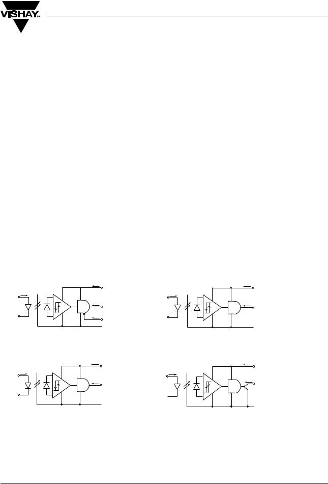
Figure 1. Schematics
Document Number 83683 |
www.vishay.com |
Rev. 1.5, 15-Apr-05 |
3 |

SFH6700/ 01/ 02/ 05/ 11/ 12/ 19
Vishay Semiconductors
Recommended Operating Conditions
A 0.1 µF bypass capacitor connected between pins 5 and 8 must be used.
Parameter |
Test condition |
Part |
Symbol |
Min |
Typ. |
Max |
Unit |
Supply voltage |
|
|
VCC |
4.5 |
|
15 |
V |
Enable voltage high |
|
SFH6700 |
VEH |
2.0 |
|
15 |
V |
|
|
SFH6719 |
VEH |
2.0 |
|
15 |
V |
Enable voltage low |
|
SFH6700 |
VEL |
0 |
|
0.8 |
V |
|
|
SFH6719 |
VEL |
0 |
|
0.8 |
V |
Forward input current |
|
|
IFon |
1.6 (1) |
|
5.0 |
mA |
|
|
|
IFoff |
|
|
0.1 |
mA |
Operating temperature |
|
|
TA |
- 40 |
|
85 |
°C |
Output pull-up resistor |
|
SFH6705 |
RL |
350 |
|
4 |
kΩ |
Fan Output |
RL = 1.0 kΩ |
SFH6705 |
N |
|
|
16 |
LS TTL |
|
|
|
|
|
|
|
Loads |
|
|
|
|
|
|
|
|
(1) We recommended using a 2.2 mA to permit at least 20 % CTR degradation guard band.
Electrical Characteristics
- 40 °C ≤ Tamb ≤ 85 °C; 4.5 V ≤ VCC ≤ 15 V; 1.6 mA ≤ IFon ≤ 5.0 mA; 2.0 ≤ VEH ≤ 15 V; 0 ≤ VEL ≤ 0.8 V; 0 mA ≤ IFoff ≤ 0.1 mA; Typical values: Tamb = 25 °C; VCC = 5.0 V; IFon = 3.0 mA unless otherwise specified
Minimum and maximum values are testing requirements. Typical values are characteristics of the device and are the result of engineering evaluation. Typical values are for information only and are not part of the testing requirements.
Input
Parameter |
Test condition |
Symbol |
Min |
Typ. |
Max |
Unit |
Forward voltage |
IF = 5.0 mA |
VF |
|
1.6 |
1.75 |
V |
|
IF = 5.0 mA, |
VF |
|
|
1.8 |
V |
Input current hysteresis |
VCC = 5.0 V, IHYS = IFon-IFon |
IHYS |
|
0.1 |
|
mA |
Reverse current |
VR = 3.0 V |
IR |
|
0.5 |
10 |
µA |
Capacitance |
VR = 0 V, f = 1.0 MHz; |
CO |
|
60 |
|
pF |
Thermal resistance |
|
Rthja |
|
700 |
|
K/W |
www.vishay.com |
Document Number 83683 |
4 |
Rev. 1.5, 15-Apr-05 |

SFH6700/ 01/ 02/ 05/ 11/ 12/ 19
Vishay Semiconductors
Output
Parameter |
Test condition |
Symbol |
Min |
Typ. |
Max |
Unit |
Logic low output voltage |
IOL = 6.4 mA |
VOL |
|
|
0.5 |
V |
Logic high output voltage |
IOH = 2.6 mA, VOH = VCC-1.8 V |
|
2.4 |
|
|
V |
(except SFH6705) |
|
|
|
|
|
|
|
|
|
|
|
|
|
Output leakage current |
VO = 5.5 V, VCC = 4.5 V, |
IOHH |
|
0.5 |
100 |
µA |
(VOUT>VCC) (except SFH6705) |
IF = 5.0 mA |
|
|
|
|
|
|
VO = 15 V, VCC = 4.5 V, |
IOHH |
|
1.0 |
500 |
µA |
|
IF = 5.0 mA |
|
|
|
|
|
Output leakage current |
VO = 5.5 V, VCC = 5.5 V, |
IOHH |
|
0.5 |
100 |
µA |
(SFH705 only) |
IF = 5.0 mA |
|
|
|
|
|
|
VO = 15 V, VCC = 15 V, |
IOHH |
|
1.0 |
500 |
µA |
|
IF = 5.0 mA |
|
|
|
|
|
Logic high enable voltage |
|
VEH |
2.0 |
|
|
V |
(SFH6700/19 only) |
|
|
|
|
|
|
|
|
|
|
|
|
|
Logic low enable voltage |
|
VEL |
|
|
0.8 |
V |
(SFH6700/19 only) |
|
|
|
|
|
|
|
|
|
|
|
|
|
Logic high enable current |
VEN = 2.7 V |
IEH |
|
|
20 |
µA |
(SFH6700/19 only) |
|
|
|
|
|
|
|
|
|
|
|
|
|
|
VEN = 5.5 V |
IEH |
|
|
100 |
µA |
|
VEN = 15 V |
IEH |
|
0.001 |
250 |
µA |
Logic low enable current |
VEN = 0.4 V |
IEL |
- 320 |
- 50 |
|
µA |
(SFH6700/19 only) |
|
|
|
|
|
|
High impedance state output |
VO = 0.4 V, VEN = 2.0 V, |
IOZL |
- 20 |
|
|
µA |
current (SFH6700/19 only) |
IF = 5.0 mA |
|
|
|
|
|
|
VO = 2.4 V, VEN = 2.0 V, |
IOZH |
|
|
20 |
µA |
|
IF = 0 mA |
|
|
|
|
|
|
VO = 5.5 V, VEN = 2.0 V, |
IOZH |
|
|
100 |
µA |
|
IF = 0 mA |
|
|
|
|
|
|
|
IOZH |
|
0.001 |
500 |
µA |
Logic low supply current |
VCC = 5.5 V, IF = 0 |
ICCL |
|
3.7 |
6.0 |
mA |
|
VCC = 15 V, IF = 0 |
ICCL |
|
4.1 |
6.5 |
mA |
Logic high supply current |
VCC = 5.5 V, IF = 5.0 mA |
ICCH |
|
3.4 |
4.0 |
mA |
|
VCC = 15V, IF = 5.0 mA |
ICCH |
|
3.7 |
5.0 |
mA |
Logic low short circuit output |
VO = VCC = 5.5 V, IF = 0 |
IOSL |
25 |
|
|
mA |
current 2) |
|
|
|
|
|
|
|
VO = VCC = 15 V, IF = 0 |
IOSL |
40 |
|
|
mA |
Logic high short circuit output |
VCC = 5.5 V, VO = 0 V, |
IOSL |
|
|
- 10 |
mA |
current 2) |
IF = 5.0 mA |
|
|
|
|
|
|
VCC = 15 V, VO = 0 V, |
IOSL |
|
|
- 25 |
mA |
|
IF = 5.0 mA |
|
|
|
|
|
Thermal resistance |
|
Rthja |
|
300 |
|
K/W |
2) Output short circuit time ≤ 10ms.
Coupler
Parameter |
Test condition |
Symbol |
Min |
Typ. |
Max |
|
Unit |
|
Capacitance (input-output) |
f = 1.0 MHz, pins 1-4 and 5-8 |
CIO |
|
0.6 |
|
|
pF |
|
|
shorted together |
|
|
|
|
|
|
|
|
|
|
|
|
|
|
|
|
Isolation resistance |
VIO = 500 |
V, Tamb = 25 °C |
RIO |
1012 |
|
|
|
Ω |
|
VIO = 500 |
V, Tamb = 100 °C |
RIO |
1011 |
|
|
|
Ω |
|
|
|
|
|
|
|
|
|
Document Number 83683 |
|
|
|
|
|
|
www.vishay.com |
|
Rev. 1.5, 15-Apr-05 |
|
|
|
|
|
|
5 |
|

SFH6700/ 01/ 02/ 05/ 11/ 12/ 19
Vishay Semiconductors
Switching Characteristics
0 °C ≤ Tamb ≤ 85 °C; 4.5 V ≤ VCC ≤ 15 V; 1.6 mA ≤ IFon ≤ 5.0 mA; 2.0 ≤ VEH ≤ 15 V (SFH6700/19); 0 ≤ VEL ≤ 0.8 V (SFH6700/19); 0 mA
≤ IFoff≤ 0.1 mA
Typical values: Tamb = 25 °C; VCC = 5.0 V; IFon = 3.0 mA unless otherwise specified. (3)
Parameter |
Test condition |
Symbol |
Min |
Typ. |
Max |
Unit |
Propagation delay time to logic |
Without peaking capacitor |
tPHL |
|
120 |
|
ns |
low output level, SFH6700/01/ |
|
|
|
|
|
|
02/11/12/19 |
|
|
|
|
|
|
|
|
|
|
|
|
|
|
With peaking capacitor |
tPHL |
|
115 |
300 |
ns |
|
|
tPLH |
|
125 |
|
ns |
|
|
tPLH |
|
90 |
300 |
ns |
Output enable time to logic high |
|
tPZH |
|
20 |
|
ns |
(SFH6700/19) |
|
|
|
|
|
|
|
|
|
|
|
|
|
Output enable time to logic low |
|
tPZL |
|
25 |
|
ns |
(SFH6700/19) |
|
|
|
|
|
|
|
|
|
|
|
|
|
Output disable time from logic |
|
tPLZ |
|
50 |
|
ns |
low (SFH6700/19) |
|
|
|
|
|
|
Output rise time |
10 % to 90 % |
tr |
|
40 |
|
ns |
Output fall time |
90 % to 10 % |
tf |
|
10 |
|
ns |
(3) A 0.1 µF bypass capacitor connected between pins 5 and 8 must be used
Typical values: Tamb = 25 °C, VCC = 5.0 V; IFon = 3.0 mA; RL = 390 Ω unless otherwise specified (3)
Parameter |
Test condition |
Part |
Symbol |
Min |
Typ. |
Max |
Unit |
Propagation delay time to logic |
Without peaking capacitor |
SFH6705 |
tPHL |
|
115 |
|
ns |
low output level |
|
|
|
|
|
|
|
|
|
|
|
|
|
|
|
|
With peaking capacitor |
SFH6705 |
tPHL |
|
105 |
300 |
ns |
|
Without peaking capacitor |
SFH6705 |
tPLH |
|
125 |
|
ns |
|
With peaking capacitor |
SFH6705 |
tPLH |
|
90 |
300 |
ns |
Output rise time |
10 % to 90 % |
|
tr |
|
25 |
|
ns |
|
90 % to 10 % |
|
tr |
|
4 |
|
ns |
www.vishay.com |
Document Number 83683 |
6 |
Rev. 1.5, 15-Apr-05 |
 Loading...