


VISHAY DG643DY, DG643DJ, DG642DY, DG642DJ, DG641DY Datasheet
...
DG641/642/643
Vishay Siliconix
Low On-Resistance Wideband/Video Switches
|
|
C |
Wide Bandwidth: 500 MHz |
High Precision |
RF and Video Switching |
Low Crosstalk at 5 MHz: ±85 dB |
Improved Frequency Response |
RGB Switching |
Low rDS(on): 5 , DG642 |
Low Insertion Loss |
Video Routing |
TTL Logic Compatible |
Improved System Performance |
Cellular Communications |
Fast Switching: tON 50 ns |
Reduced Board Space |
ATE |
Single Supply Compatibility |
Low Power Consumption |
Radar/FLIR Systems |
High Current: 100 mA, DG642 |
|
Satellite Receivers |
|
|
Programmable Filters |
D C |
|
|
The DG641/642/643 are high performance monolithic video switches designed for switching wide bandwidth analog and digital signals. DG641 is a quad SPST, DG642 is a single SPDT, and DG643 is a dual SPDT function. These devices have exceptionally low on-resistances (5 typÐDG642), low capacitance and high current handling capability.
To achieve TTL compatibility, low channel capacitances and fast switching times, the DG641/642/643 are built on the Vishay Siliconix proprietary D/CMOS process. Each switch conducts equally well in both directions when on, and blocks up to 14 Vp-p when off. An epitaxial layer prevents latchup.

 C C D G D C G
Dual-In-Line and SOIC |
Dual-In-Line and SOIC |
IN1 |
1 |
16 |
IN2 |
D1 |
2 |
15 |
D2 |
S1 |
3 |
14 |
S2 |
V± |
4 |
13 |
V+ |
GND |
|
DG641 |
GND |
5 |
12 |
||
S4 |
6 |
11 |
S3 |
D4 |
7 |
10 |
D3 |
IN4 |
8 |
9 |
IN3 |
Top View
S1 1
D1 2
V± 3
GND 4
Dual-In-Line and SOIC |
|
8 |
IN |
7 |
V+ |
|
|
6 |
D2 |
5 |
S2 |
DG642 |
|
Top View |
|
IN1 |
1 |
|
16 |
IN2 |
D1 |
2 |
|
15 |
D2 |
GND |
3 |
|
14 |
GND |
|
|
|
||
S1 |
4 |
|
13 |
S2 |
V± |
5 |
|
12 |
V+ |
|
|
|
||
S4 |
6 |
|
11 |
S3 |
GND |
7 |
|
10 |
GND |
|
|
|
||
D4 |
8 |
DG643 |
9 |
D3 |
|
|
|
|
Top View
DG |
|
DG |
|
DG |
||||||||
|
|
|
|
|
|
|
|
|
|
|
|
|
Logic |
|
Switch |
|
Logic |
SW1 |
|
SW2 |
|
Logic |
SW1, SW2 |
|
SW3, SW4 |
|
|
|
|
|
|
|
|
|
|
|
|
|
0 |
|
OFF |
|
0 |
OFF |
|
ON |
|
0 |
OFF |
|
ON |
|
|
|
|
|
|
|
|
|
|
|
|
|
1 |
|
ON |
|
1 |
ON |
|
OFF |
|
1 |
ON |
|
OFF |
|
|
|
|
|
|
|
|
|
|
|
|
|
|
Logic ª0º 0.8 V |
|
Logic ª0º 0.8 V |
|
|
|
Logic ª0º 0.8 V |
|
||||
|
Logic ª1º 2.4 V |
|
Logic ª1º 2.4 V |
|
|
|
Logic ª1º 2.4 V |
|
||||
|
|
|
|
|
|
|
|
|
|
|
||
Document Number: 70058 |
|
|
|
|
|
www.vishay.com FaxBack 408-970-5600 |
||||||
S-52433ÐRev. E, 06-Sep-99 |
|
|
|
|
|
|
|
|
4-1 |
|||

DG641/642/643
Vishay Siliconix
ORDERING INFORMATION
Temp Range |
Package |
Part Number |
|
|
|
|
|
DG641 |
|
|
|
|
|
|
|
±40 to 85_C |
16-Pin Plastic DIP |
DG641DJ |
|
|
|
||
16-Pin Narrow SOIC |
DG641DY |
||
|
|||
|
|
|
|
DG642 |
|
|
|
|
|
|
|
±40 to 85_C |
8-Pin Plastic DIP |
DG642DJ |
|
|
|
||
8-Pin Narrow SOIC |
DG642DY |
||
|
|||
|
|
|
|
DG643 |
|
|
|
|
|
|
|
±40 to 85_C |
16-Pin Plastic DIP |
DG643DJ |
|
|
|
||
|
16-Pin Narrow SOIC |
DG643DY |
ABSOLUTE MAXIMUM RATINGS
V+ to V± . . . . . . . . . . . . . . . . . . . . . . . . . . . . . . . . . . . . . . . . . . . . . ±0.3 V to 21 V V+ to GND . . . . . . . . . . . . . . . . . . . . . . . . . . . . . . . . . . . . . . . . . . . ±0.3 V to 21 V V± to GND . . . . . . . . . . . . . . . . . . . . . . . . . . . . . . . . . . . . . . . . . ±19 V to +0.3 V Digital Inputs . . . . . . . . . . . . . . . . . . . . . . . . . . . . . . . (V±) ±0.3 V to (V+) +0.3 V or 20 mA, whichever occurs first
VS, VD . . . . . . . . . . . . . . . . . . . . . . . . . . . . . . . . . . . . . (V±) ±0.3 V to (V±) +14 V or 20 mA, whichever occurs first
Continuous Current (Any Terminal Except S or D) . . . . . . . . . . . . . . . . 20 mA Continuous Current S or D: DG641/643 . . . . . . . . . . . . . . . . . . . . . . . 75 mA DG642 . . . . . . . . . . . . . . . . . . . . . . . . . . 100 mA
Current, S or D (Pulsed 1 ms, 10% duty cycle max)
DG641/643 . . . . . . . . . . . . . . . . . . . . . . 200 mA DG642 . . . . . . . . . . . . . . . . . . . . . . . . . . 300 mA
Storage Temperature . . . . . . . . . . . . . . . . . . . . . . . . . . . . . . . . . . ±65 to 125_C Power Dissipation (Package)b
8-Pin Plastic DIP and Narrow SOICc . . . . . . . . . . . . . . . . . . . . . . . . . . 300 mW 16-Pin Plastic DIPd . . . . . . . . . . . . . . . . . . . . . . . . . . . . . . . . . . . . . . . . . 470 mW 16-Pin Narrow SOICe . . . . . . . . . . . . . . . . . . . . . . . . . . . . . . . . . . . . . . . 600 mW
Notes:
a.Signals on SX, DX, or INX exceeding V+ or V± will be clamped by internal diodes. Limit forward diode current to maximum current ratings.
b.All leads welded or soldered to PC Board.
c.Derate 7.6 mW/_C above 75_C
d.Derate 6 mW/_C above 75_C
e.Derate 80 mW/_C above 75_C

 SCHEMATIC DIAGRAM (TYPICAL CHANNEL)
V+ |
|
|
GND |
5 V |
S |
Reg |
|
|
|
|
|
IN |
|
|
|
|
D |
V± |
|
|
FIGURE 1.
www.vishay.com S FaxBack 408-970-5600 |
Document Number: 70058 |
4-2 |
S-52433ÐRev. E, 06-Sep-99 |
DG641/642/643
Vishay Siliconix
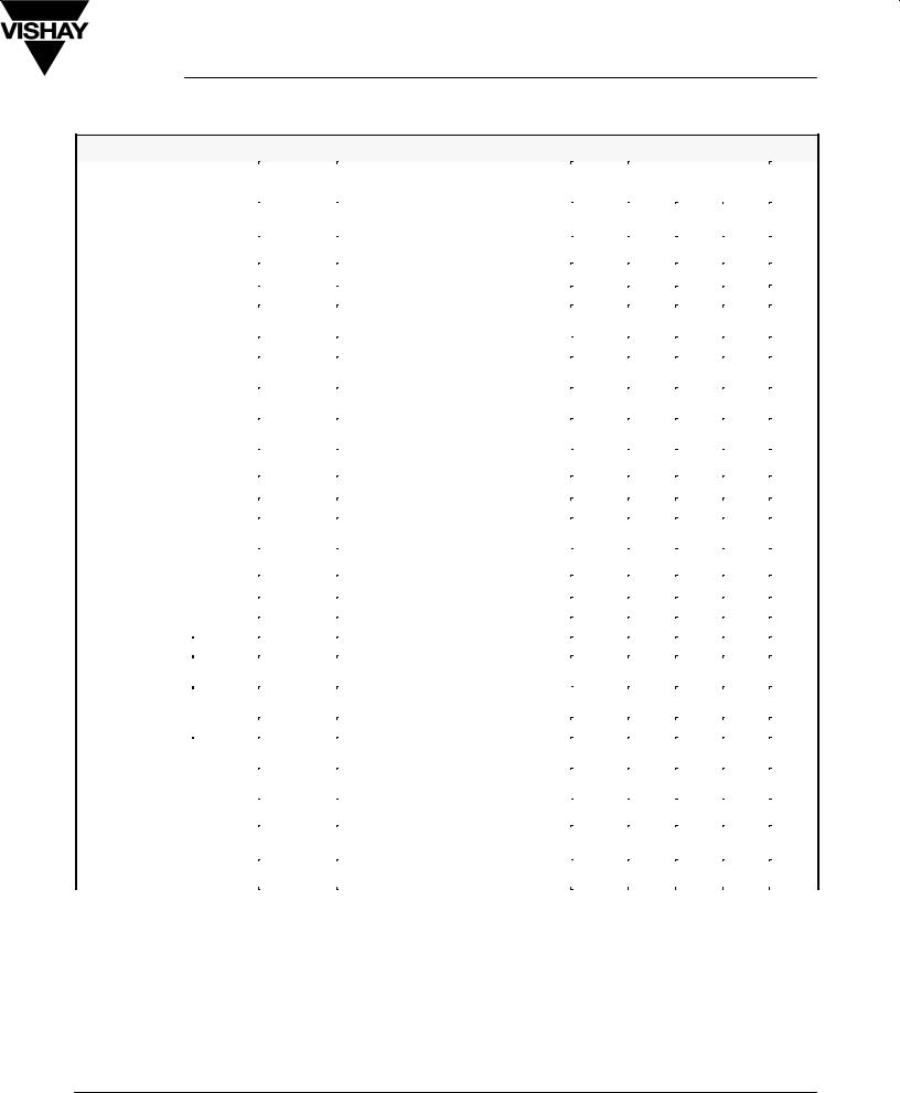
SPECIFICATIONS FOR DG64 AND DG643
|
|
|
Test Conditions |
|
|
|
Limits |
|
|
|||||
|
|
Unless Otherwise Specified |
|
|
±40 to 85_C |
|
|
|||||||
|
|
|
V+ = 15 V, V± = ±3 V |
|
|
|
|
|
|
|
||||
Parameter |
Symbol |
|
Tempa |
Minb |
|
Typc |
|
Maxb |
Unit |
|||||
V |
= 2.4 V, V |
INL |
= 0.8 Ve |
|
|
|||||||||
|
|
|
INH |
|
|
|
|
|
|
|
|
|
|
|
Analog Switch |
|
|
|
|
|
|
|
|
|
|
|
|
|
|
|
|
|
|
|
|
|
|
|
|
|
||||
Analog Signal Rangedd |
V |
|
V± = ±5 V, V+ = 12 V |
Full |
±5 |
|
|
|
8 |
V |
||||
|
|
|
|
|
|
|
|
|
|
|
|
|||
|
ANALOG |
|
V± = GND, V+ = 12 V |
Full |
0 |
|
|
|
8 |
|
||||
|
|
|
|
|
|
|
||||||||
|
|
|
|
|
|
|
|
|
|
|
|
|
|
|
Drain-Source On-Resistance |
rDS(on) |
|
|
|
|
|
|
Room |
|
|
8 |
|
15 |
|
|
IS = ±10 mA, VD = 0 V |
Full |
|
|
|
|
20 |
W |
||||||
rDS(on) Match |
DrDS(on) |
|
|
|
|
|
|
Room |
|
|
1 |
|
2 |
|
Source Off Leakage Current |
IS(off) |
|
VS = 0 V, VD = 10 V |
Room |
±10 |
|
±0.02 |
|
10 |
|
||||
|
Full |
±100 |
|
|
|
100 |
|
|||||||
Drain Off Leakage Current |
ID(off) |
|
VS = 10 V, VD = 0V |
Room |
±10 |
|
±0.02 |
|
10 |
nA |
||||
|
Full |
±100 |
|
|
|
100 |
||||||||
Channel On Leakage Current |
ID(on) |
|
VS = VD = 0 V |
Room |
±10 |
|
±0.1 |
|
10 |
|
||||
|
Full |
±100 |
|
|
|
100 |
|
|||||||
Digital Control |
|
|
|
|
|
|
|
|
|
|
|
|
|
|
|
|
|
|
|
|
|
|
|
|
|
|
|
|
|
Input Voltage High |
VINH |
|
|
|
|
|
|
Full |
2.4 |
|
|
|
|
V |
Input Voltage Low |
VINL |
|
|
|
|
|
|
Full |
|
|
|
|
0.8 |
|
Input Current |
IIN |
|
VIN = GND or V+ |
Room |
±1 |
|
0.05 |
|
1 |
mA |
||||
|
Full |
±20 |
|
|
|
20 |
||||||||
Dynamic Characteristics |
|
|
|
|
|
|
|
|
|
|
|
|
|
|
|
|
|
|
|
|
|
|
|
|
|
|
|||
On State Input Capacitanced |
C |
|
V = V |
D |
= 0 V |
Room |
|
|
10 |
|
20 |
|
||
|
S(on) |
|
S |
|
|
|
|
|
|
|
|
|
|
|
Off State Input Capacitanced |
C |
|
V |
= 0 V |
|
Room |
|
|
4 |
|
12 |
pF |
||
|
S(off) |
|
S |
|
|
|
|
|
|
|
|
|
|
|
Off State Output Capacitanced |
C |
|
V |
= 0 V |
|
Room |
|
|
4 |
|
12 |
|
||
|
D(off) |
|
D |
|
|
|
|
|
|
|
|
|
|
|
Bandwidth |
BW |
RL = 50 W, See Figure 6 |
Room |
|
|
500 |
|
|
MHz |
|||||
Turn On Time |
tON |
|
|
|
|
|
|
Room |
|
|
50 |
|
70 |
|
RL = 1 kW, CL = 35 pF, |
See Figure 2 |
Full |
|
|
|
|
140 |
ns |
||||||
Turn Off Time |
tOFF |
Room |
|
|
28 |
|
50 |
|||||||
|
|
|
|
|
|
|
|
|
|
|||||
|
|
|
|
|
|
Full |
|
|
|
|
85 |
|
||
Charge Injection |
Q |
CL = 1000 pF, VD = 0 V, See Figure 3 |
Room |
|
|
±19 |
|
|
pC |
|||||
Off Isolation |
OIRR |
RIN = 75 W, RL = 75 W, f = 5 MHz |
Room |
|
|
±60 |
|
|
|
|||||
|
|
|
See Figure 4 |
|
|
|
|
|
|
dB |
||||
|
|
|
|
|
|
|
|
|
|
|
|
|
|
|
All Hostile Crosstalk |
XTALK(AH) |
RIN = 10 W, RL = 75 W, f = 5 MHz |
Room |
|
|
±87 |
|
|
|
|||||
|
See Figure 5 |
|
|
|
|
|
||||||||
Power Supplies |
|
|
|
|
|
|
|
|
|
|
|
|
|
|
|
|
|
|
|
|
|
|
|
|
|
|
|
|
|
Positive Supply Current |
I+ |
|
|
|
|
|
|
Room |
|
|
3.5 |
|
6 |
|
|
|
|
|
|
|
Full |
|
|
|
|
9 |
|
||
|
|
|
VIN = 0 V or VIN = 5 V |
|
|
|
|
mA |
||||||
|
|
|
|
|
|
|
|
|
||||||
Negative Supply Current |
I± |
|
Room |
±6 |
|
±3 |
|
|
||||||
|
|
|
|
|
|
|
|
|
|
|||||
|
|
|
|
|
|
Full |
±9 |
|
|
|
|
|
||
|
|
|
|
|
|
|
|
|
|
|
|
|
||
|
|
|
|
|
|
|
|
|
|
|
|
|
|
|
Notes:
a.Room = 25_C, Full = as determined by the operating temperature suffix.
b.Typical values are for DESIGN AID ONLY, not guaranteed nor subject to production testing.
c.The algebraic convention whereby the most negative value is a minimum and the most positive a maximum, is used in this data sheet.
d.Guaranteed by design, not subject to production test.
e.VIN = input voltage to perform proper function.
Document Number: 70058 |
www.vishay.com S FaxBack 408-970-5600 |
S-52433ÐRev. E, 06-Sep-99 |
4-3 |
 Loading...