


VS-VSKD56..
VS-VSKD56.., VS-VSKE56.., VS-VSKJ56.., VS-VSKC56..
Vishay Semiconductors
Revision: 05-Apr-16
1
Document Number: 94625
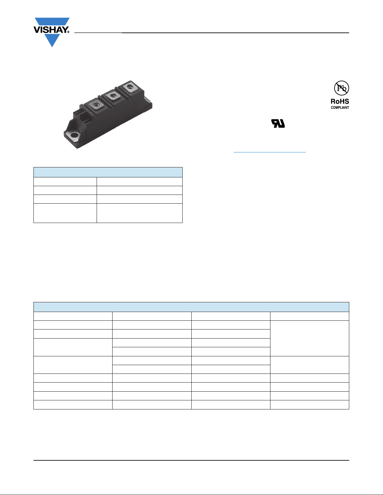
ADD-A-PAK Gen 7
Power Modules Standard Diodes, 60 A
MECHANICAL DESCRIPTION
The ADD-A-PAK Gen 7, new generation of ADD-A-PAK
module, combines the excellent thermal performances
obtained by the usage of exposed direct bonded copper
substrate, with advanced compact simple package solution
and simplified internal structure with minimized number of
interfaces.
FEATURES
• High voltage
• Industrial standard package
• Low thermal resistance
• UL approved file E78996
• Designed and qualified for industrial level
• Material categorization: for definitions of compliance
please see www.vishay.com/doc?99912
BENEFITS
• Excellent thermal performances obtained by the usage of
exposed direct bonded copper substrate
• Up to 1600 V
• High surge capability
• Easy mounting on heat sink
ELECTRICAL DESCRIPTION
These modules are intended for general purpose high
voltage applications such as high voltage regulated power
supplies, lighting circuits, temperature and motor speed
control circuits, UPS and battery charger.
PRODUCT SUMMARY
I
F(AV)
60 A
Type Modules - Diode, High Voltage
Package ADD-A-PAK Gen 7
Circuit
Two diodes doubler circuit, two
diodes common cathode, two diodes
common anode, single diode
ADD-A-PAK
MAJOR RATINGS AND CHARACTERISTICS
SYMBOL CHARACTERISTICS VALUES UNITS
I
F(AV)
114 °C 60
A
I
F(RMS)
94
I
FSM
50 Hz 1300
60 Hz 1360
I
2
t
50 Hz 8.44
kA
2
s
60 Hz 7.68
I
2
t 84.5 kA
2
s
V
RRM
Range 400 to 1600 V
T
J
-40 to +150 °C
T
Stg
-40 to +150 °C
VS-VSKD56.., VS-VSKE56.., VS-VSKJ56.., VS-VSKC56..
Vishay Semiconductors
Revision: 05-Apr-16
2
Document Number: 94625
ELECTRICAL SPECIFICATIONS
VOLTAGE RATINGS
TYPE NUMBER
VOLTAGE
CODE
V
RRM
, MAXIMUM REPETITIVE
PEAK REVERSE VOLTAGE
V
V
RSM
, MAXIMUM NON-REPETITIVE
PEAK REVERSE VOLTAGE
V
I
RRM
MAXIMUM
AT T
J
= 150 °C
mA
VS-VSK.56
04 400 500
10
06 600 700
08 800 900
10 1000 1100
12 1200 1300
14 1400 1500
16 1600 1700
FORWARD CONDUCTION
PARAMETER SYMBOL TEST CONDITIONS VALUES UNITS
Maximum average forward current
at case temperature
I
F(AV)
180° conduction, half sine wave
60 A
114 °C
Maximum RMS forward current I
F(RMS)
DC at 90 °C case temperature 94
A
Maximum peak, one-cycle forward,
non-repetitive surge current
I
FSM
t = 10 ms
No voltage
reapplied
Sinusoidal half wave,
initial T
J
= T
J
maximum
1300
t = 8.3 ms 1360
t = 10 ms
100 % V
RRM
reapplied
1090
t = 8.3 ms 1140
Maximum I
2
t for fusing I
2
t
t = 10 ms
No voltage
reapplied
8.44
kA
2
s
t = 8.3 ms 7.68
t = 10 ms
100 % V
RRM
reapplied
5.97
t = 8.3 ms 5.43
Maximum I
2
t for fusing I
2
t t = 0.1 ms to 10 ms, no voltage reapplied 84.5 kA
2
s
Low level value of threshold voltage V
F(TO)1
(16.7 % x x I
F(AV)
< I < x I
F(AV)
), T
J
= T
J
maximum 0.74
V
High level value of threshold voltage V
F(TO)2
(I > x I
F(AV)
), T
J
= T
J
maximum 0.86
Low level value of forward
slope resistance
r
f1
(16.7 % x x I
F(AV)
< I < x I
F(AV)
), T
J
= T
J
maximum 3.94
m
High level value of forward
slope resistance
r
f2
(I > x I
F(AV)
), T
J
= T
J
maximum 3.43
Maximum forward voltage drop V
FM
I
FM
= x I
F(AV)
, T
J
= 25 °C, t
p
= 400 μs square wave 1.6 V
BLOCKING
PARAMETER SYMBOL TEST CONDITIONS VALUES UNITS
Maximum peak reverse
leakage current
I
RRM
T
J
= 150 °C 10 mA
Maximum RMS insulation voltage V
INS
50 Hz
3000 (1 min)
3600 (1 s)
V
VS-VSKD56.., VS-VSKE56.., VS-VSKJ56.., VS-VSKC56..
Vishay Semiconductors
Revision: 05-Apr-16
3
Document Number: 94625
Note
• Table shows the increment of thermal resistance R
thJC
when devices operate at different conduction angles than DC
THERMAL AND MECHANICAL SPECIFICATIONS
PARAMETER SYMBOL TEST CONDITIONS VALUES UNITS
Junction and storage temperature range T
J
, T
Stg
-40 to +150 °C
Maximum internal thermal resistance,
junction to case per leg
R
thJC
DC operation 0.33
°C/W
Typical thermal resistance,
case to heat sink per module
R
thCS
Mounting surface flat, smooth and greased 0.1
Mounting torque ± 10 %
to heatsink
A mounting compound is recommended and the
torque should be rechecked after a period of
3 hours to allow for the spread of the compound.
4
Nm
busbar 3
Approximate weight
75 g
2.7 oz.
Case style JEDEC
®
ADD-A-PAK Gen 7 (TO-240AA)
R CONDUCTION PER JUNCTION
DEVICES
SINE HALF WAVE CONDUCTION RECTANGULAR WAVE CONDUCTION
UNITS
180° 120° 90° 60° 30° 180° 120° 90° 60° 30°
VSK.56 0.115 0.136 0.173 0.236 0.346 0.09 0.145 0.185 0.243 0.349 °C/W
 Loading...