


Vishay TSOP31230, TSOP31233, TSOP31236, TSOP31238, TSOP31240 User guide
...TSOP312.., TSOP314..
www.vishay.com |
Vishay Semiconductors |
|
IR Receiver Modules for Remote Control Systems
FEATURES
• Very low supply current
• Photo detector and preamplifier in one package
• Internal filter for PCM frequency
• Improved shielding against EMI
• Supply voltage: 2.5 V to 5.5 V
• Improved immunity against ambient light
1
2 |
• Insensitive to supply voltage ripple and noise |
94 8691
3
MECHANICAL DATA
Pinning:
1 = GND, 2 = VS, 3 = OUT
• Material categorization:
For definitions of compliance please see www.vishay.com/doc?99912
DESCRIPTION
The TSOP312.., TSOP314..series are miniaturized IR receiver modules for infrared remote control systems. A PIN diode and a preamplifier are assembled on a leadframe, the epoxy package contains an IR filter.
The demodulated output signal can be directly connected to a microprocessor for decoding.
The TSOP312.., TSOP314.. are optimized to suppress almost all spurious pulses from energy saving lamps like CFLs. The AGC4 used in the TSOP314.. may suppress some data signals. The TSOP312.. is a legacy product for all common IR remote control data formats. Between these two receiver types, the TSOP314.. is preferred. Customers should initially try the TSOP314.. in their design.
These components have not been qualified according to automotive specifications.
PARTS TABLE
AGC |
|
LEGACY, FOR |
|
RECOMMENDED FOR |
|
LONG BURST REMOTE CONTROLS (AGC2) |
|
LONG BURST CODES (AGC4) (1) |
|
|
|
|
||
|
30 kHz |
TSOP31230 |
|
TSOP31430 |
|
|
|
|
|
|
33 kHz |
TSOP31233 |
|
TSOP31433 |
|
|
|
|
|
Carrier |
36 kHz |
TSOP31236 |
|
TSOP31436 (2)(3)(4) |
frequency |
38 kHz |
TSOP31238 |
|
TSOP31438 (5)(6) |
|
40 kHz |
TSOP31240 |
|
TSOP31440 |
|
|
|
|
|
|
56 kHz |
TSOP31256 |
|
TSOP31456 (7)(8) |
Package |
|
Cast |
|
|
|
|
|
||
Pinning |
|
1 = GND, 2 = VS, 3 = OUT |
||
Dimensions (mm) |
10.0 W x 12.5 H x 5.8 D |
|||
|
|
|
|
|
Mounting |
|
Leaded |
|
|
|
|
|
|
|
Application |
|
Remote control |
|
|
|
|
|||
Best remote control code |
(2) RC-5 (3) RC-6 (4) Panasonic (5) NEC (6) Sharp (7) r-step (8) Thomson RCA |
|||
Note
(1) We advise try AGC4 first if the burst length is unknown.
Rev. 1.1, 05-Feb-14 |
1 |
Document Number: 82492 |
THIS DOCUMENT IS SUBJECT TO CHANGE WITHOUT NOTICE. THE PRODUCTS DESCRIBED HEREIN AND THIS DOCUMENT ARE SUBJECT TO SPECIFIC DISCLAIMERS, SET FORTH AT www.vishay.com/doc?91000
TSOP312.., TSOP314..
www.vishay.com |
Vishay Semiconductors |
|
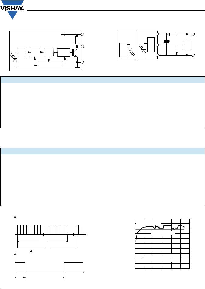
BLOCK DIAGRAM
16832 |
|
|
|
|
|
|
|
|
2 |
|
|
|
|
VS |
|
|
|
|
30 kΩ |
|
|
|
|
3 |
Input |
AGC |
Band |
Demo- |
OUT |
|
||||
pass |
dulator |
|
||
|
|
|
||
|
|
|
|
1 |
PIN |
|
Control circuit |
|
GND |
APPLICATION CIRCUIT |
|
|
|
|
17170_5 |
|
|
R1 |
|
Transmitter |
|
|
|
|
IR receiver |
|
|
|
|
with |
|
VS |
|
+ VS |
TSALxxxx |
|
C1 |
||
| <![if ! IE]> <![endif]>Circuit |
|
|
||
|
OUT |
|
||
|
µC |
|
||
|
|
|
|
|
|
|
GND |
VO |
GND |
|
|
|
|
|
R1 and C1 are recommended for protection against EOS. |
|
|||
Components should be in the range of 33 Ω < R1 < 1 kΩ, |
|
|||
C1 > 0.1 µF. |
|
|
|
|
ABSOLUTE MAXIMUM RATINGS
PARAMETER |
TEST CONDITION |
SYMBOL |
VALUE |
UNIT |
|
Supply voltage (pin 2) |
|
VS |
-0.3 to |
+6.0 |
V |
Supply current (pin 2) |
|
IS |
3 |
|
mA |
Output voltage (pin 3) |
|
VO |
-0.3 to (VS + 0.3) |
V |
|
Output current (pin 3) |
|
IO |
5 |
|
mA |
Junction temperature |
|
Tj |
100 |
°C |
|
Storage temperature range |
|
Tstg |
-25 to |
+85 |
°C |
Operating temperature range |
|
Tamb |
-25 to |
+85 |
°C |
Power consumption |
Tamb ≤ 85 °C |
Ptot |
10 |
|
mW |
Soldering temperature |
t ≤ 10 s, 1 mm from case |
Tsd |
260 |
°C |
|
Note
•Stresses beyond those listed under “Absolute Maximum Ratings” may cause permanent damage to the device. This is a stress rating only and functional operation of the device at these or any other conditions beyond those indicated in the operational sections of this specification is not implied. Exposure to absolute maximum rating conditions for extended periods may affect the device reliability.
ELECTRICAL AND OPTICAL CHARACTERISTICS (Tamb = 25 °C, unless otherwise specified)
PARAMETER |
TEST CONDITION |
SYMBOL |
MIN. |
TYP. |
MAX. |
UNIT |
|
|
|
|
|
|
|
Supply current (pin 2) |
Ev = 0, VS = 3.3 V |
ISD |
0.27 |
0.35 |
0.45 |
mA |
Ev = 40 klx, sunlight |
ISH |
|
0.45 |
|
mA |
|
|
|
|
||||
Supply voltage |
|
VS |
2.5 |
|
5.5 |
V |
Transmission distance |
Ev = 0, test signal see fig. 1, |
d |
|
45 |
|
m |
IR diode TSAL6200, IF = 200 mA |
|
|
||||
|
|
|
|
|
|
|
Output voltage low (pin 3) |
IOSL = 0.5 mA, Ee = 0.7 mW/m2, test signal see fig. 1 |
VOSL |
|
|
100 |
mV |
Minimum irradiance |
Pulse width tolerance: |
Ee min. |
|
0.12 |
0.25 |
mW/m2 |
tpi - 5/fo < tpo < tpi + 6/fo, test signal see fig. 1 |
|
|||||
|
|
|
|
|
|
|
Maximum irradiance |
tpi - 5/fo < tpo < tpi + 6/fo, test signal see fig. 1 |
Ee max. |
30 |
|
|
W/m2 |
Directivity |
Angle of half transmission distance |
ϕ1/2 |
|
± 45 |
|
deg |
TYPICAL CHARACTERISTICS (Tamb = 25 °C, unless otherwise specified)
Ee Optical Test Signal
(IR diode TSAL6200, IF = 0.4 A, 30 pulses, f = f0, t = 10 ms)
|
|
|
|
|
|
|
|
|
|
t |
|
|
|
|
|
|
tpi * |
|
|
|
|
|
|
|
|
|
|
|
T |
|
|
|
|
* tpi |
|
10/f0 is recommended for optimal function |
|||||||
VO |
Output Signal |
|
|
|
|
|
|
16110 |
||
|
1) |
7/f |
|
< t |
|
< 15/f |
|
|
||
VOH |
2) |
|
0 |
d |
|
0 |
|
|
||
t |
pi |
- 5/f |
0 |
< t |
< t |
+ 6/f |
0 |
|||
|
|
|
|
|
po |
pi |
|
|||
VOL
td 1) |
tpo 2) |
t |
Fig. 1 - Output Active Low
|
1.0 |
|
|
|
|
|
|
|
0.9 |
Output Pulse Width |
|
|
|
|
|
| <![if ! IE]> <![endif]>(ms) |
|
|
|
|
|
|
|
0.8 |
|
|
|
|
|
|
|
| <![if ! IE]> <![endif]>Width |
|
|
|
|
|
|
|
0.6 |
|
Input Burst Length |
|
|
|||
|
0.7 |
|
|
|
|||
| <![if ! IE]> <![endif]>Pulse |
0.5 |
|
|
|
|
|
|
|
|
|
|
|
|
|
|
| <![if ! IE]> <![endif]>Output- |
0.4 |
|
|
|
|
|
|
0.3 |
|
λ = 950 nm, |
|
|
|
||
|
|
|
|
|
|
|
|
| <![if ! IE]> <![endif]>po |
0.2 |
Optical Test Signal, Fig.1 |
|
|
|||
|
|
|
|||||
|
|
|
|
|
|
|
|
| <![if ! IE]> <![endif]>t |
0.1 |
|
|
|
|
|
|
|
|
|
|
|
|
|
|
|
0 |
|
|
|
103 |
104 |
105 |
|
0.1 |
1 |
10 |
102 |
|||
20752 |
Ee - Irradiance (mW/m2) |
Fig. 2 - Pulse Length and Sensitivity in Dark Ambient
Rev. 1.1, 05-Feb-14 |
2 |
Document Number: 82492 |
THIS DOCUMENT IS SUBJECT TO CHANGE WITHOUT NOTICE. THE PRODUCTS DESCRIBED HEREIN AND THIS DOCUMENT ARE SUBJECT TO SPECIFIC DISCLAIMERS, SET FORTH AT www.vishay.com/doc?91000

TSOP312.., TSOP314..
www.vishay.com |
Vishay Semiconductors |
|
Optical Test Signal
Ee
600 µs |
600 µs |
t |
|
||
|
t = 60 ms |
|
Output Signal, (see fig. 4) |
94 8134 |
VO
VOH |
|
|
VOL |
|
t |
ton |
toff |
| <![if ! IE]> <![endif]>) |
4 |
|
|
|
|
|
|
| <![if ! IE]> <![endif]>2 |
|
Correlation with Ambient Light Sources: |
|
||||
| <![if ! IE]> <![endif]>(mW/m |
|
|
|||||
3.5 |
10 W/m2 = 1.4 kLx (Std. illum. A, T = 2855 K) |
|
|||||
|
10 W/m2 = 8.2 kLx (Daylight, T = 5900 K) |
|
|||||
3 |
|
|
|
|
|
|
|
| <![if ! IE]> <![endif]>Irradiance |
|
|
|
|
|
|
|
2.5 |
Wavelength of Ambient |
|
|
||||
Illumination: λ = 950 nm |
|
|
|||||
|
|
|
|||||
2 |
|
|
|
|
|
|
|
| <![if ! IE]> <![endif]>- Threshold |
|
|
|
|
|
|
|
1.5 |
|
|
|
|
|
|
|
1 |
|
|
|
|
|
|
|
|
|
|
|
|
|
|
|
| <![if ! IE]> <![endif]>e min. |
0.5 |
|
|
|
|
|
|
|
|
|
|
|
|
|
|
| <![if ! IE]> <![endif]>E |
0 |
|
|
|
|
|
|
|
|
|
|
|
|
|
|
|
0.01 |
|
0.1 |
1 |
10 |
100 |
|
20757 |
E |
e |
- Ambient DC Irradiance (W/m2) |
|
|||
|
|
|
|
|
|||
Fig. 3 - Output Function
|
0.8 |
|
|
|
|
|
| <![if ! IE]> <![endif]>(ms) |
0.7 |
|
|
|
Ton |
|
|
|
|
|
|
||
|
|
|
|
|
|
|
| <![if ! IE]> <![endif]>Width |
0.6 |
|
|
|
|
|
|
|
|
|
|
|
|
| <![if ! IE]> <![endif]>Pulse |
0.5 |
|
|
|
|
|
0.4 |
|
|
|
Toff |
|
|
| <![if ! IE]> <![endif]>- Output |
|
|
|
|
|
|
0.3 |
|
|
|
|
|
|
0.2 |
|
|
|
|
|
|
| <![if ! IE]> <![endif]>off |
|
|
|
|
|
|
|
|
|
|
|
|
|
| <![if ! IE]> <![endif]>T |
|
λ = 950 nm, |
|
|
|
|
| <![if ! IE]> <![endif]>, |
0.1 |
|
|
|
||
| <![if ! IE]> <![endif]>on |
Optical Test Signal, Fig. 3 |
|
|
|||
| <![if ! IE]> <![endif]>T |
0 |
|
|
|
|
|
|
|
|
|
|
|
|
|
0.1 |
1 |
10 |
100 |
1000 |
10 000 |
20759 |
|
Ee - Irradiance (mW/m2) |
|
|||
Fig. 4 - Output Pulse Diagram
|
1.2 |
|
|
|
|
|
|
|
|
|
|
|
|
|
|
|
|
|
|
|
|
| <![if ! IE]> <![endif]>Responsivity |
1.0 |
|
|
|
|
|
|
|
|
|
|
|
|
|
|
|
|
|
|
||
0.8 |
|
|
|
|
|
|
|
|
|
|
|
|
|
|
|
|
|
|
|
|
|
| <![if ! IE]> <![endif]>- Rel. |
0.6 |
|
|
|
|
|
|
|
|
|
|
|
|
|
|
|
|
|
|
||
0.4 |
|
|
|
|
|
|
|
|
|
|
| <![if ! IE]> <![endif]>e |
|
|
|
|
|
|
|
|
|
|
|
|
|
|
|
|
|
|
|
||
| <![if ! IE]> <![endif]>/E |
|
|
|
|
|
|
|
|
|
|
| <![if ! IE]> <![endif]>min. |
0.2 |
|
|
|
|
f = f0 ± 5 % |
|
|
|
|
| <![if ! IE]> <![endif]>e |
|
|
|
|
f(3 dB) = f0/10 |
|
|
|
||
| <![if ! IE]> <![endif]>E |
|
|
|
|
|
|
|
|
||
|
0.0 |
|
|
|
|
|
|
|
|
|
|
|
|
|
|
|
|
|
|
|
|
|
0.7 |
0.9 |
1.1 |
|
1.3 |
|||||
16925 |
|
|
f/f0 - Relative Frequency |
|
|
|||||
Fig. 5 - Frequency Dependence of Responsivity
Fig. 6 - Sensitivity in Bright Ambient
| <![if ! IE]> <![endif]>) |
3.0 |
|
|
|
| <![if ! IE]> <![endif]>2 |
|
|
|
|
| <![if ! IE]> <![endif]>(mW/m |
2.5 |
|
|
|
|
|
|
|
|
| <![if ! IE]> <![endif]>Irradiance |
2.0 |
f = f0 |
|
|
|
f = 30 kHz |
|
|
|
1.5 |
f = 10 kHz |
|
|
|
f = 100 Hz |
|
|
||
| <![if ! IE]> <![endif]>hold |
|
|
|
|
1.0 |
|
|
|
|
| <![if ! IE]> <![endif]>Thres |
|
|
|
|
0.5 |
|
|
|
|
| <![if ! IE]> <![endif]>- |
|
|
|
|
|
|
|
|
|
| <![if ! IE]> <![endif]>e min. |
0 |
|
|
|
| <![if ! IE]> <![endif]>E |
1 |
10 |
100 |
1000 |
|
VS RMS - AC Voltage on DC Supply Voltage (mV)
Fig. 7 - Sensitivity vs. Supply Voltage Disturbances
|
1 |
|
|
|
|
|
|
|
0.9 |
|
|
|
|
|
|
| <![if ! IE]> <![endif]>Cycle |
0.8 |
|
|
|
|
|
|
0.7 |
|
|
|
|
|
|
|
| <![if ! IE]> <![endif]>Duty |
|
|
|
|
|
|
|
0.6 |
|
|
|
|
|
|
|
|
|
|
|
|
|
|
|
| <![if ! IE]> <![endif]>Envelope |
0.5 |
|
|
|
|
|
|
0.4 |
|
|
|
|
TSOP312.. |
|
|
|
|
|
|
|
|
||
0.3 |
|
|
|
|
|
|
|
| <![if ! IE]> <![endif]>Max. |
|
|
|
|
|
|
|
0.2 |
|
|
TSOP314.. |
|
|
||
|
|
|
|
|
|
|
|
|
0.1 |
f = 38 kHz, Ee = 2 mW/m² |
|
|
|
||
|
0 |
|
|
|
|||
|
|
|
|
|
|
|
|
|
0 |
20 |
40 |
60 |
80 |
100 |
120 |
20773 |
Burst Length (number of cycles/burst) |
Fig. 8 - Maximum Envelope Duty Cycle vs. Burst Length
Rev. 1.1, 05-Feb-14 |
3 |
Document Number: 82492 |
THIS DOCUMENT IS SUBJECT TO CHANGE WITHOUT NOTICE. THE PRODUCTS DESCRIBED HEREIN AND THIS DOCUMENT ARE SUBJECT TO SPECIFIC DISCLAIMERS, SET FORTH AT www.vishay.com/doc?91000
 Loading...