VISHAY TSDF1250, TSDF1250R, TSDF1250W, TSDF1250RW Technical data

TSDF1250
TSDF1250/TSDF1250R/TSDF1250W/TSDF1250RW
Vishay Telefunken
Silicon NPN Planar RF Transistor
|
|
Electrostatic sensitive device. |
|
|
|
Observe precautions for handling. |
|
Applications |
|
|
|
For low noise applicatins such as power amplifiers, |
frequencies. |
|
|
mixers and oscillators in analogue and digital TV±sys- |
|
|
|
tems (e.g. satellite tuners) up to microwave |
|
|
|
Features |
|
|
|
D Low power applications |
D High transition frequency fT = 12 GHz |
||
D Very low noise figure |
D Excellent large signal behaviour |
||
2 |
1 |
1 |
2 |
|
94 9279 |
13 579 |
|
94 9278 |
95 10831 |
3 |
|
4 |
4 |
|
3 |
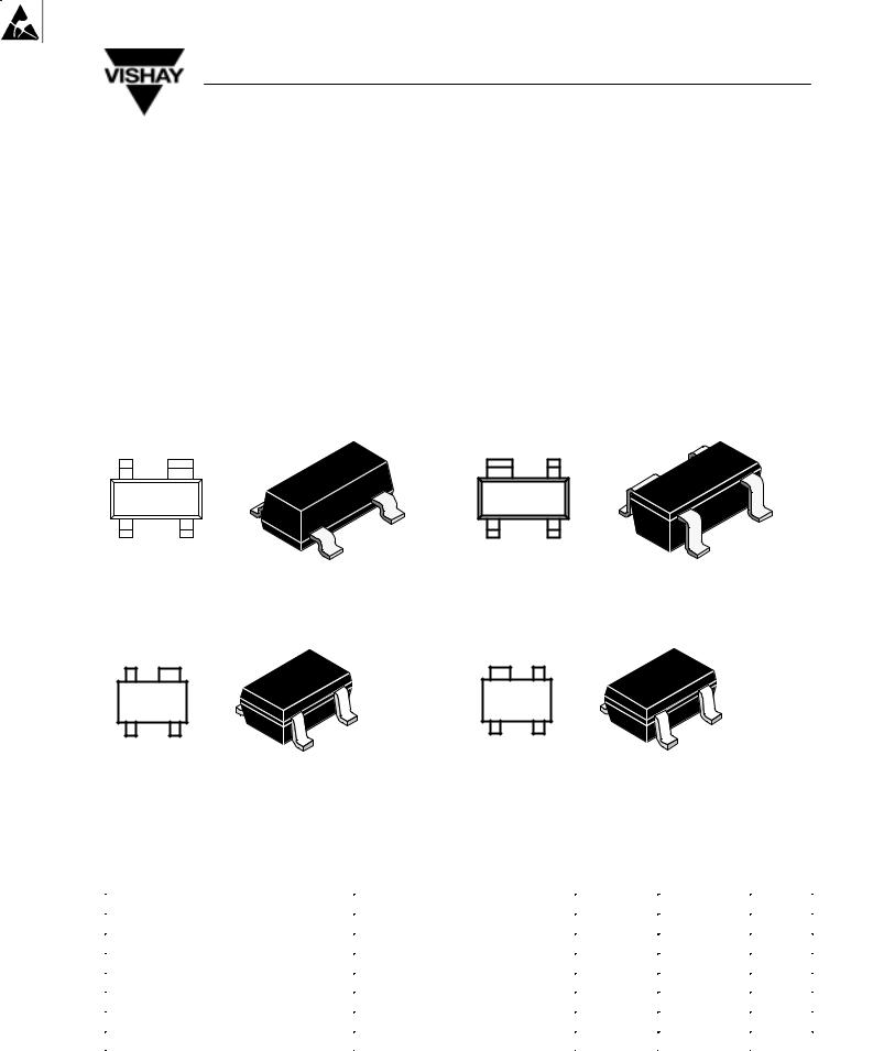
TSDF1250 Marking: F50 |
TSDF1250R Marking: 50F |
||||
Plastic case (SOT 143) |
Plastic case (SOT 143R) |
||||
1 = Collector, 2 = Emitter, 3 = Base, 4 = Emitter |
1 = Collector, 2 = Emitter, 3 = Base, 4 = Emitter |
||||
2 |
1 |
|
1 |
2 |
|
|
13 653 |
13 566 |
|
13 654 |
13 566 |
3 |
4 |
|
4 |
3 |
|
TSDF1250W Marking: WF5 |
|
TSDF1250RW Marking: W5F |
|
||
Plastic case (SOT 343) |
|
Plastic case (SOT 343R) |
|
||
1 = Collector, 2 = Emitter, 3 = Base, 4 = Emitter |
1 = Collector, 2 = Emitter, 3 = Base, 4 = Emitter |
||||
Absolute Maximum Ratings
Tamb = 25_C, unless otherwise specified
Parameter |
Test Conditions |
|
Symbol |
Value |
Unit |
|
Collector-base voltage |
|
|
VCBO |
9 |
V |
|
Collector-emitter voltage |
|
|
VCEO |
6 |
V |
|
Emitter-base voltage |
|
|
VEBO |
2 |
V |
|
Collector current |
|
|
IC |
60 |
mA |
|
Total power dissipation |
Tamb ≤ 60 °C |
|
Ptot |
200 |
mW |
|
Junction temperature |
|
|
Tj |
150 |
°C |
|
Storage temperature range |
|
|
Tstg |
±65 to +150 |
°C |
|
|
|
|
|
|
|
|
Document Number 85067 |
|
www.vishay.de •FaxBack +1-408-970-5600 |
|
|||
Rev. 5, 08-Jul-99 |
|
|
|
|
1 (6) |
|

TSDF1250/TSDF1250R/TSDF1250W/TSDF1250RW
Vishay Telefunken
Maximum Thermal Resistance
Tamb = 25_C, unless otherwise specified
Parameter |
Test Conditions |
Symbol |
Value |
Unit |
Junction ambient |
on glass fibre printed board (25 x 20 x 1.5) mm3 |
R |
450 |
K/W |
|
plated with 35mm Cu |
thJA |
|
|
|
|
|
|
Electrical DC Characteristics
Tamb = 25_C, unless otherwise specified
Parameter |
Test Conditions |
Symbol |
Min |
Typ |
Max |
Unit |
Collector cut-off current |
VCE = 12 V, VBE = 0 |
ICES |
|
|
100 |
mA |
Collector-base cut-off current |
VCB = 10 V, IE = 0 |
ICBO |
|
|
100 |
nA |
Emitter-base cut-off current |
VEB = 1 V, IC = 0 |
IEBO |
|
|
2 |
mA |
Collector-emitter breakdown voltage |
IC = 1 mA, IB = 0 |
V(BR)CEO |
6 |
|
|
V |
Collector-emitter saturation voltage |
IC = 50 mA, IB = 5 mA |
VCEsat |
|
0.1 |
0.5 |
V |
DC forward current transfer ratio |
VCE = 5 V, IC = 40 mA |
hFE |
50 |
100 |
150 |
|
Electrical AC Characteristics
Tamb = 25_C, unless otherwise specified
Parameter |
|
Test Conditions |
Symbol |
Min |
Typ |
Max |
Unit |
|||
Transition frequency |
VCE = 5 |
V, IC = |
40 mA, f = 1 GHz |
fT |
|
12 |
|
GHz |
||
Collector-base capacitance |
VCB = 1 |
V, f = 1 MHz |
Ccb |
|
0.6 |
|
pF |
|||
Collector-emitter capacitance |
VCE = 1 |
V, f = 1 MHz |
Cce |
|
0.3 |
|
pF |
|||
Emitter-base capacitance |
VEB = 0.5 V, f = 1 MHz |
Ceb |
|
0.7 |
|
pF |
||||
Noise figure |
VCE = 5 |
V, IC = |
5 mA, |
F |
|
1.2 |
|
dB |
||
|
ZS = ZSopt, ZL = 50 W, f = 2 GHz |
|
|
|
|
|
||||
Power gain |
VCE = 5 |
V, IC = |
5 mA, |
Gpe |
|
11 |
|
dB |
||
|
f = 2 GHz (@Fopt) |
|
|
|
|
|
||||
|
VCE = 5 |
V, IC = |
40 mA, |
Gpe |
|
13.5 |
|
dB |
||
|
ZS = ZSopt, ZL = 50 W, f = 2 GHz |
|
|
|
|
|
||||
Transducer gain |
V = 5 |
V, I |
C |
= |
40 mA, |
S 2 |
|
12.5 |
|
dB |
|
CE |
|
|
|
21e |
|
|
|
|
|
|
Z0 = 50 W, f = 2 GHz |
|
|
|
|
|
||||
Third order intercept point at |
VCE = 5 |
V, IC = |
40 mA, f = 2 GHz |
IP3 |
|
28 |
|
dBm |
||
output |
|
|
|
|
|
|
|
|
|
|
www.vishay.de •FaxBack +1-408-970-5600 |
Document Number 85067 |
2 (6) |
Rev. 5, 08-Jul-99 |
 Loading...