


IRFR9020, IRFU9020, SiHFR9020, SiHFU9020
www.vishay.com |
Vishay Siliconix |
|
|
|
Power MOSFET |
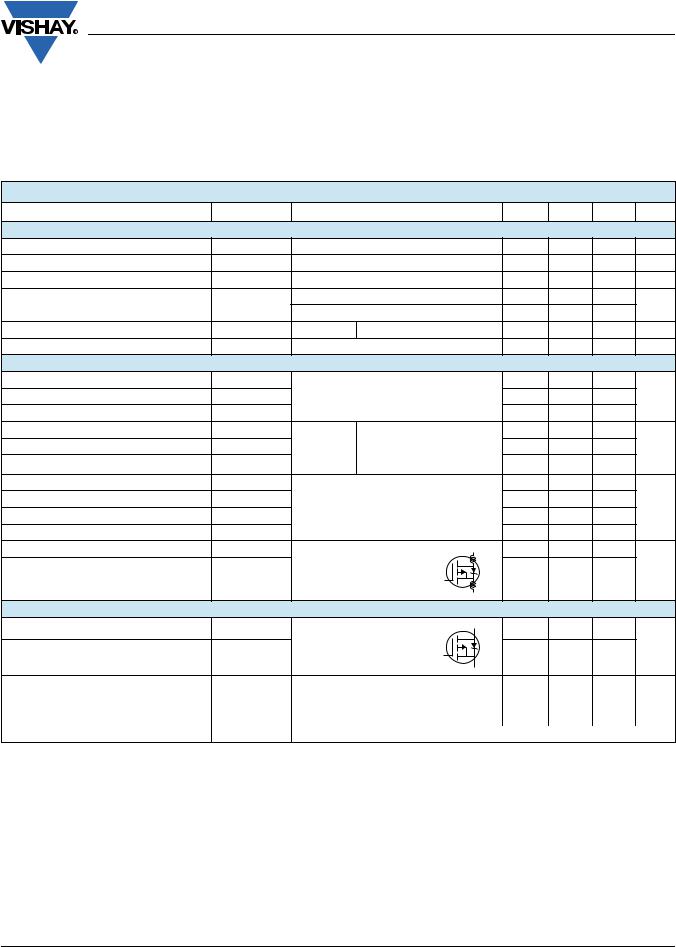
PRODUCT SUMMARY
VDS (V) |
- 50 |
|
|
RDS(on) ( ) |
VGS = - 10 V |
|
0.28 |
Qg (Max.) (nC) |
14 |
|
|
Qgs (nC) |
6.5 |
|
|
Qgd (nC) |
6.5 |
|
|
Configuration |
Single |
|
|
|
|
|
|
S
FEATURES
• Surface Mountable (Order As IRFR9020,
SiHFR9020)
• Straight Lead Option (Order As IRFU9020,
SiHFU9020)
• Repetitive Avalanche Ratings
• Dynamic dV/dt Rating
• Simple Drive Requirements
•Ease of Paralleling
•Material categorization: For definitions of compliance please see www.vishay.com/doc?99912
DPAK |
IPAK |
|
|
|
(TO-252) |
(TO-251) |
|
G |
|
|
D |
|
||
D |
|
|
||
|
|
|
||
G |
S |
D |
S |
|
G |
||||
|
|
|
D
P-Channel MOSFET
DESCRIPTION
The power MOSFET technology is the key to Vishay’s advanced line of power MOSFET transistors. The efficient geometry and unique processing of this latest “State of the Art” design achieves: very low on-state resistance combined with high transconductance; superior reverse energy and diode recovery dV/dt.
The power MOSFET transistors also feature all of the well established advantages of MOSFET’S such as voltage control, very fast switching, ease of paralleling and temperature stability of the electrical parameters.
Surface mount packages enhance circuit performance by reducing stray inductances and capacitance. The TO-252 surface mount package brings the advantages of power MOSFET’s to high volume applications where PC board surface mounting is desirable. The surface mount option IRFR9020, SiHFR9020 is provided on 16mm tape. The straight lead option IRFU9020, SiHFU9020 of the device is called the IPAK (TO-251).
They are well suited for applications where limited heat dissipation is required such as, computers and peripherals, telecommunication equipment, DC/DC converters, and a wide range of consumer products.
ORDERING INFORMATION
Package |
DPAK (TO-252) |
DPAK (TO-252) |
DPAK (TO-252) |
IPAK (TO-251) |
|
Lead (Pb)-free and Halogen-free |
SiHFR9020-GE3 |
SiHFR9020TR-GE3a |
SiHFR9020TRL-GE3a |
SiHFU9020-GE3 |
|
Lead (Pb)-free |
IRFR9020PbF |
IRFR9020TRPbFa |
IRFR9020TRLPbFa |
IRFU9020PbF |
|
SiHFR9020-E3 |
SiHFR9020T-E3a |
SiHFR9020TL-E3a |
SiHFU9020-E3 |
||
|
Note
a. See device orientation.
ABSOLUTE MAXIMUM RATINGS (TC = 25 °C, unless otherwise noted)
PARAMETER |
|
|
SYMBOL |
LIMIT |
UNIT |
|
|
|
|
|
|
|
|
Drain-Source Voltage |
|
|
VDS |
- 50 |
V |
|
Gate-Source Voltage |
|
|
VGS |
± 20 |
||
|
|
|
||||
Continuous Drain Current |
|
VGS at - 10 V |
TC = 25 °C |
ID |
- 9.9 |
|
|
TC = 100 °C |
- 6.3 |
A |
|||
|
|
|
|
|||
Pulsed Drain Currenta |
|
|
IDM |
- 40 |
|
|
Linear Derating Factor |
|
|
|
0.33 |
W/°C |
|
|
|
|
|
|
|
|
Single Pulse Avalanche Energyb |
|
|
EAS |
250 |
mJ |
|
Repetitive Avalanche Currenta |
|
|
IAR |
- 9.9 |
A |
|
Repetitive Avalanche Energya |
|
|
EAR |
4.2 |
mJ |
|
Maximum Power Dissipation |
|
TC = 25 °C |
PD |
42 |
W |
|
Peak Diode Recovery dV/dtc |
|
|
dV/dt |
5.8 |
V/ns |
|
Operating Junction and Storage Temperature Range |
|
|
TJ, Tstg |
- 55 to + 150 |
°C |
|
Soldering Recommendations (Peak Temperature)d |
|
for 10 s |
|
300 |
||
|
|
|
||||
Notes
a.Repetitive rating; pulse width limited by maximum junction temperature (see fig. 16).
b.VDD = - 25 V, Starting TJ = 25 °C, L = 5.1 mH, Rg = 25 , Peak IL = - 9.9 A
c.ISD - 9.9 A, dI/dt -120 A/μs, VDD 40 V, TJ 150 °C.
d.0.063" (1.6 mm) from case.
e.When mounted on 1" square PCB (FR-4 or G-10 material).
S13-0169-Rev. D, 04-Feb-13 |
1 |
Document Number: 90350 |
|
For technical questions, contact: hvm@vishay.com |
|
THIS DOCUMENT IS SUBJECT TO CHANGE WITHOUT NOTICE. THE PRODUCTS DESCRIBED HEREIN AND THIS DOCUMENT ARE SUBJECT TO SPECIFIC DISCLAIMERS, SET FORTH AT www.vishay.com/doc?91000
IRFR9020, IRFU9020, SiHFR9020, SiHFU9020
www.vishay.com |
|
|
|
|
Vishay Siliconix |
|
|
|
|
|
|
||
|
|
|
|
|
|
|
THERMAL RESISTANCE RATINGS |
|
|
|
|
|
|
PARAMETER |
SYMBOL |
MIN. |
TYP. |
MAX. |
|
UNIT |
|
|
|
|
|
|
|
Maximum Junction-to-Ambient |
RthJA |
- |
- |
110 |
|
|
Case-to-Sink |
RthCS |
- |
1.7 |
- |
|
°C/W |
Maximum Junction-to-Case (Drain) |
RthJC |
- |
- |
3.0 |
|
|
SPECIFICATIONS (TJ = 25 °C, unless otherwise noted)
PARAMETER |
SYMBOL |
TEST CONDITIONS |
MIN. |
TYP. |
MAX. |
UNIT |
|||
Static |
|
|
|
|
|
|
|
|
|
Drain-Source Breakdown Voltage |
VDS |
VGS = 0 V, ID = - 250 μA |
- 50 |
- |
- |
V |
|||
Gate-Source Threshold Voltage |
VGS(th) |
VDS = VGS, ID = - 250 μA |
- 2.0 |
- |
- 4.0 |
V |
|||
Gate-Source Leakage |
IGSS |
|
VGS = ± 20 V |
|
- |
- |
± 500 |
nA |
|
Zero Gate Voltage Drain Current |
IDSS |
VDS = max. rating, VGS = 0 V |
- |
- |
250 |
μA |
|||
VDS = 0.8 x max. rating, VGS = 0 V, TJ = 125 °C |
- |
- |
1000 |
||||||
|
|
|
|||||||
Drain-Source On-State Resistance |
RDS(on) |
VGS = - 10 V |
ID = 5.7 Ab |
- |
0.20 |
0.28 |
|
||
Forward Transconductance |
gfs |
VDS - 50 V, IDS = - 5.7 A |
2.3 |
3.5 |
- |
S |
|||
Dynamic |
|
|
|
|
|
|
|
|
|
Input Capacitance |
Ciss |
|
VGS = 0 V, |
|
- |
490 |
- |
|
|
Output Capacitance |
Coss |
|
VDS = - 25 V, |
|
- |
320 |
- |
pF |
|
Reverse Transfer Capacitance |
Crss |
f = 1.0 MHz, see fig. 9 |
- |
70 |
- |
|
|||
|
|
|
|
||||||
Total Gate Charge |
Qg |
|
ID = - 9.7 A, VDS = 0.8 x max. |
- |
9.4 |
14 |
|
||
Gate-Source Charge |
Qgs |
VGS = - 10 V |
rating, see fig. 18 |
- |
4.3 |
6.5 |
nC |
||
(Independent operating |
|||||||||
Gate-Drain Charge |
Qgd |
|
- |
4.3 |
6.5 |
|
|||
|
temperature) |
|
|||||||
Turn-On Delay Time |
td(on) |
VDD = - 25 V, ID = - 9.7 A, |
- |
8.2 |
12 |
|
|||
Rise Time |
tr |
- |
57 |
66 |
|
||||
Rg = 18 , RD = 2.4 , see fig. 17 |
ns |
||||||||
Turn-Off Delay Time |
td(off) |
- |
12 |
18 |
|||||
(Independent operating temperature) |
|
||||||||
Fall Time |
tf |
Between lead, |
|
- |
25 |
38 |
|
||
Internal Drain Inductance |
LD |
D |
- |
4.5 |
- |
|
|||
|
|
6 mm (0.25") from |
|
|
|
|
nH |
||
Internal Source Inductance |
LS |
package and center of |
G |
- |
7.5 |
- |
|||
die contact. |
|
|
|
||||||
|
|
|
|
|
|
|
|
||
|
|
|
|
S |
|
|
|
|
|
Drain-Source Body Diode Characteristics |
|
|
|
|
|
|
|
|
|
Continuous Source-Drain Diode Current |
IS |
MOSFET symbol |
D |
- |
- |
- 9.9 |
|
||
|
|
showing the |
|
|
|
|
|
A |
|
Pulsed Diode Forward Currenta |
ISM |
integral reverse |
G |
- |
- |
- 40 |
|||
|
|||||||||
p - n junction diode |
S |
|
|||||||
Body Diode Voltage |
VSD |
TJ = 25 °C, IS = - 9.9 A, VGS = 0 |
Vb |
- |
- |
- 6.3 |
V |
|
Body Diode Reverse Recovery Time |
trr |
TJ = 25 °C, IF = - 9,7 A, dI/dt = 100 |
A/μsb |
56 |
110 |
280 |
ns |
|
Body Diode Reverse Recovery Charge |
Qrr |
0.17 |
0.34 |
0.85 |
nC |
|||
|
|
|||||||
Forward Turn-On Time |
ton |
Intrinsic turn-on time is negligible (turn-on is dominated by LS and LD) |
|
|||||
Notes
a.Repetitive rating; pulse width limited by maximum junction temperature (see fig. 16).
b.Pulse width 300 μs; duty cycle 2 %.
S13-0169-Rev. D, 04-Feb-13 |
2 |
Document Number: 90350 |
|
For technical questions, contact: hvm@vishay.com |
|
THIS DOCUMENT IS SUBJECT TO CHANGE WITHOUT NOTICE. THE PRODUCTS DESCRIBED HEREIN AND THIS DOCUMENT ARE SUBJECT TO SPECIFIC DISCLAIMERS, SET FORTH AT www.vishay.com/doc?91000

IRFR9020, IRFU9020, SiHFR9020, SiHFU9020
www.vishay.com |
Vishay Siliconix |
|
TYPICAL CHARACTERISTICS (25 °C, unless otherwise noted)
Fig. 1 - Typical Output Characteristics |
|
Fig. 4 - Maximum Safe Operating Area |
|
|
|
|
|||
|
|
|
|
|
|
|
|
|
|
|
|
|
|
|
|
|
|
|
|
Fig. 2 - Typical Transfer Characteristics |
Fig. 5 - Typical Transconductance vs. Drain Current |
|
Fig. 3 - Typical Saturation Characteristics |
Fig. 6 - Typical Source-Drain Diode Forward Voltage |
|
S13-0169-Rev. D, 04-Feb-13 |
3 |
Document Number: 90350 |
|
For technical questions, contact: hvm@vishay.com |
|
THIS DOCUMENT IS SUBJECT TO CHANGE WITHOUT NOTICE. THE PRODUCTS DESCRIBED HEREIN AND THIS DOCUMENT ARE SUBJECT TO SPECIFIC DISCLAIMERS, SET FORTH AT www.vishay.com/doc?91000

IRFR9020, IRFU9020, SiHFR9020, SiHFU9020
www.vishay.com |
Vishay Siliconix |
|
|
|
|
|
|
|
|
|
|
|
|
|
|
|
|
|
|
|
|
|
|
|
|
|
Fig. 7 - Breakdown Voltage vs. Temperature |
|
|
Fig. 9 - Typical Capacitance vs. Drain-to-Source Voltage |
|
|||
|
|
|
|
|
|
|
|
|
|
|
|
|
|
|
|
|
|
|
|
|
|
|
|
Fig. 8 - Normalized On-Resistance vs. Temperature |
Fig. 10 - Typical Gate Charge vs. Gate-to-Source Voltage |
S13-0169-Rev. D, 04-Feb-13 |
4 |
Document Number: 90350 |
|
For technical questions, contact: hvm@vishay.com |
|
THIS DOCUMENT IS SUBJECT TO CHANGE WITHOUT NOTICE. THE PRODUCTS DESCRIBED HEREIN AND THIS DOCUMENT ARE SUBJECT TO SPECIFIC DISCLAIMERS, SET FORTH AT www.vishay.com/doc?91000
 Loading...