


Vishay Si9182DH-12-T1, Si9182DH-15-T1, Si9182DH-18-T1, Si9182DH-25-T1, Si9182DH-28-T1 Schematic [ru]
...
Si9182
Vishay Siliconix
Micropower 250-mA CMOS LDO Regulator
With Error Flag/Power-On-Reset
FEATURES
D Low 105-mV Dropout at 250-mA Load |
|
D Fixed 1.215-V, 1.5-V, 1.8-V, 2.5-V, 2.8-V, 2.9-V, |
D Guaranteed 250-mA Output Current |
|
3.0-V, 3.3-V, 5.0-V, or Adjustable Output Voltage |
D 500-mA Peak Output Current Capability |
Available |
Options |
|
D Other Output Voltages Available by Special Order |
|
D Uses Low ESR Ceramic Output Capacitor |
|
|
|
|
|
D Fast Load and Line Transient Response |
|
APPLICATIONS |
D Only 100-mV(rms) Noise With Noise Bypass |
|
|
Capacitor |
|
D Cellular Phones |
D 1-mA Maximum Shutdown Current |
|
|
|
D Laptop and Palm Computers |
|
D Built-in Short Circuit and Thermal Protection |
|
|
|
D PDA, Digital Still Cameras |
|
D Out-Of-Regulation Error Flag (Power Good or POR) |
|
|
|
|
|
DESCRIPTION |
|
|
The Si9182 is a 250-mA CMOS LDO (low dropout) voltage |
LDO’s output noise for low noise applications. |
|
regulator. The device features ultra low ground current and |
|
|
dropout voltage to prolong battery life in portable electronics. |
The Si9182 also includes an out-of-regulation error flag. When |
|
The Si9182 offers line/load transient response and ripple |
||
rejection superior to that of bipolar or BiCMOS LDO regulators. |
the output voltage is 5% below its nominal output voltage, the |
|
The device is designed to maintain regulation while delivering |
error flag output goes low. If a capacitor is connected to the |
|
500-mA peak current. This is useful for systems that have high |
device’s delay pin, the error flag output pin will generate a |
|
surge current upon turn-on. The Si9182 is designed to drive |
delayed power-on-reset signal. |
|
the lower cost ceramic, as well as tantalum, output capacitors. |
The Si9182 is available in both standard and lead (Pb)-free |
|
The device is guaranteed stable from maximum load current |
||
down to 0-mA load. In addition, an external noise bypass |
MSOP-8 packages and is specified to operate over the |
|
capacitor connected to the device’s CNOISE pin will lower the |
industrial temperature range of −40 _C to 85 _C. |
|
TYPICAL APPLICATIONS CIRCUITS
|
1 |
C |
SD |
8 |
|
|
1 |
C |
|
SD |
8 |
|
|
|
NOISE |
|
|
|
|
|
NOISE |
|
|
|
|
|
2 |
DELAY |
ERROR |
7 |
|
|
2 |
DELAY |
|
ERROR |
7 |
|
|
3 |
GND |
SENSE/ADJ |
6 |
VOUT |
|
3 |
GND |
SENSE/ADJ |
6 |
|
|
V |
4 |
V |
V |
5 |
|
V |
4 |
V |
|
V |
5 |
V |
|
IN |
OUT |
|
|
|
IN |
|
OUT |
|
|||
IN |
|
|
|
|
|
IN |
|
|
|
|
|
OUT |
2.2 mF |
|
Si9182 |
|
2.2 mF |
2.2 mF |
|
Si9182 |
|
2.2 mF |
|||
GND |
|
|
|
|
|
GND |
|
|
|
|
|
|
FIGURE 1. Fixed Output |
|
|
|
|
|
FIGURE 2. Adjustable Output |
|
1 |
C |
|
SD |
8 |
ON/OFF |
|
|
NOISE |
|
|
|
|
0.1 mF |
2 |
DELAY |
|
ERROR |
7 |
POR |
|
0.1 mF |
|
|
|
|
1 MW |
|
3 |
GND |
SENSE/ADJ |
6 |
V |
|
|
|
|
|
|
|
OUT |
V |
4 |
V |
|
V |
5 |
|
|
IN |
|
OUT |
|
|
|
IN |
|
|
|
|
|
|
2.2 mF |
|
Si9182 |
|
2.2 mF |
||
GND |
|
|
|
|
|
|
FIGURE 3. Low Noise, Full Features Application
Document Number: 71150 |
www.vishay.com |
S-50955—Rev. H, 16-May-05 |
1 |

Si9182
Vishay Siliconix
ABSOLUTE MAXIMUM RATINGS
Input Voltage, VIN . . . . . . . . . . . . . . . . . . . . . . . . . . . . . . . . . . . . . . . . . . . . 6.5 V SD Input Voltage, VSD . . . . . . . . . . . . . . . . . . . . . . . . . . . . . . . . . −0.3 V to VIN Output Current, IOUT . . . . . . . . . . . . . . . . . . . . . . . . . . Short Circuit Protected Output Voltage, VOUT . . . . . . . . . . . . . . . . . . . . . . . . −0.3 V to VO(nom) + 0.3 V Maximum Junction Temperature, TJ(max) . . . . . . . . . . . . . . . . . . . . . . . 150_C Storage Temperature, TSTG . . . . . . . . . . . . . . . . . . . . . . . . . . −55_C to 150_C ESD (Human Body Model) . . . . . . . . . . . . . . . . . . . . . . . . . . . . . . . . . . . . . 2 kV
Power Dissipation (Package)a
8-Pin MSOP . . . . . . . . . . . . . . . . . . . . . . . . . . . . . . . . . . . . . . . . . . . . . 666 mW
Thermal Impedance (QJA)
8-Pin MSOPb . . . . . . . . . . . . . . . . . . . . . . . . . . . . . . . . . . . . . . . . . . . . . 150_C/W
Notes
a.Device mounted with all leads soldered or welded to PC board.
b.Derate 6.6 mW/_C above TA = 25_C
Stresses beyond those listed under “Absolute Maximum Ratings” may cause permanent damage to the device. These are stress ratings only, and functional operation of the device at these or any other conditions beyond those indicated in the operational sections of the specifications is not implied. Exposure to absolute maximum rating conditions for extended periods may affect device reliability.
RECOMMENDED OPERATING RANGE
Input Voltage, VIN . . . . . . . . . . . . . . . . . . . . . . . . . . . . . . . . . . . . . . . . 2 V to 6 V Output Voltage, VOUT (Adjustable Version) . . . . . . . . . . . . . . . . . . 1.5 V to 5 V SD Input Voltage, VSD . . . . . . . . . . . . . . . . . . . . . . . . . . . . . . . . . . . . 0 V to VIN
CIN = 2.2 mF, COUT = 2.2 mF (ceramic, X5R or X7R type) , CNOISE = 0.1 mF (ceramic) COUTRange = 1 mF to 10 mF ("10%, x5R or x7R type)
CIN w COUT
Operating Ambient Temperature, TA . . . . . . . . . . . . . . . . . . . . −40_C to 85_C Operating Junction Temperature, TJ . . . . . . . . . . . . . . . . . . . −40_C to 125_C
SPECIFICATIONS
|
|
|
|
Test Conditions |
|
|
|
Limits |
|
|
|||
|
|
|
|
Unless Otherwise Specified |
|
|
−40 to 85_C |
|
|
||||
|
|
|
|
VIN = VOUT(nom) + 1 V, IOUT = 1 mA |
|
|
|
|
|
|
|
||
Parameter |
|
Symbol |
Tempa |
Minb |
|
Typc |
|
Maxb |
Unit |
||||
|
CIN = 2.2 mF, COUT = 2.2 mF, V |
SD |
= 1.5 V |
|
|
||||||||
|
|
|
|
|
|
|
|
|
|
|
|
||
Output Voltage Range |
|
|
|
Adjustable Version |
Full |
1.5 |
|
|
|
5 |
V |
||
|
|
|
|
|
|
|
|
|
|
|
|
|
|
Output Voltage Accuracy |
|
VOUT |
1 mA v IOUT v 250 mA |
Room |
−1.5 |
|
|
|
1.5 |
% VO(nom) |
|||
(Fixed Versions) |
|
|
|
Full |
−2.5 |
|
|
|
2.5 |
||||
|
|
|
|
|
|
|
|
|
|
||||
|
|
|
|
|
|
|
|
|
|
|
|
|
|
Feedback Voltage (ADJ Version) |
|
VADJ |
|
|
|
Room |
1.191 |
|
1.215 |
|
1.239 |
V |
|
|
|
|
|
|
|
|
|
|
|
||||
|
|
|
Full |
1.179 |
|
|
|
1.251 |
|||||
|
|
|
|
|
|
|
|
|
|
|
|||
|
|
|
|
|
|
|
|
|
|
|
|
||
Line Regulation |
|
|
|
From VIN = VOUT(nom) + 1 V |
Full |
−0.18 |
|
|
|
0.18 |
|
||
(Except 5-V Version) |
|
|
|
to VOUT(nom) + 2 V |
|
|
|
|
|
|
|
||
|
|
DVOUT 100 |
|
|
|
|
|
|
|
|
|
||
Line Regulation (5-V Version) |
|
From VIN = 5.5 V to 6 V |
Full |
−0.18 |
|
|
|
0.18 |
%/V |
||||
|
|
VIN VOUT(nom) |
|
|
|
|
|
|
|
|
|
||
Line Regulation (ADJ Version) |
|
VOUT = 1.5 V, From VIN = 2.5 V to 3.5 V |
Full |
−0.18 |
|
|
|
0.18 |
|
||||
|
|
|
|
|
|
|
|||||||
|
|
|
VOUT = 5 V, From VIN = 5.5 V to 6 V |
Full |
−0.18 |
|
|
|
0.18 |
|
|||
|
|
|
|
|
|
|
|
||||||
|
|
|
|
IOUT = 10 mA |
Room |
|
|
5 |
|
20 |
|
||
Dropout Voltaged |
|
|
|
IOUT = 200 mA |
Room |
|
|
85 |
|
180 |
|
||
(@VOUT w 2 V) |
|
|
|
IOUT = 250 mA |
Room |
|
|
105 |
|
275 |
|
||
|
|
VIN − VOUT |
Full |
|
|
|
|
400 |
mV |
||||
|
|
|
|
|
|
|
|
|
|||||
|
|
|
|
IOUT = 200 mA |
Room |
|
|
170 |
|
250 |
|
||
Dropout Voltaged |
|
|
|
|
|
|
|
|
|
|
|
|
|
|
|
|
|
|
|
Room |
|
|
210 |
|
300 |
|
|
(@VOUT t 2 V, VIN w 2 V) |
|
|
|
IOUT = 250 mA |
|
|
|
|
|||||
|
|
|
|
|
|
|
|
|
|
||||
|
|
|
Full |
|
|
|
|
450 |
|
||||
|
|
|
|
|
|
|
|
|
|||||
|
|
|
|
|
|
|
|
|
|
|
|
||
|
|
|
|
|
|
|
|
|
|
|
|
||
|
|
|
|
IOUT = 0 mA |
Room |
|
|
150 |
|
|
|
||
|
|
|
|
IOUT = 200 mA |
Room |
|
|
1000 |
|
|
|
||
|
|
|
|
|
|
|
|
|
|
|
|||
Ground Pin Current |
|
IGND |
Full |
|
|
|
|
1500 |
mA |
||||
|
|
|
|
|
|
|
|
||||||
|
|
|
|
IOUT = 250 mA |
Room |
|
|
1200 |
|
|
|
||
|
|
|
|
|
|
|
|
|
|
|
|||
|
|
|
|
Full |
|
|
|
|
1900 |
|
|||
|
|
|
|
|
|
|
|
|
|
|
|
||
|
|
|
|
|
|
|
|
|
|
|
|
|
|
|
|
|
|
|
|
|
|
|
|
|
|
|
|
www.vishay.com |
Document Number: 71150 |
2 |
S-50955—Rev. H, 16-May-05 |

Si9182
Vishay Siliconix
SPECIFICATIONS
|
|
|
|
|
|
Test Conditions |
|
|
|
|
Limits |
|
|
||||||||||||
|
|
|
|
Unless Otherwise Specified |
|
|
−40 to 85_C |
|
|
||||||||||||||||
|
|
|
|
VIN = VOUT(nom) + 1 V, IOUT = 1 mA |
|
|
|
|
|
|
|
||||||||||||||
|
|
Parameter |
Symbol |
Tempa |
Minb |
|
Typc |
|
Maxb |
Unit |
|||||||||||||||
|
|
CIN = 2.2 mF, COUT = 2.2 mF, V |
SD |
= 1.5 V |
|
|
|||||||||||||||||||
|
|
|
|
|
|
|
|
|
|
|
|
|
|
|
|
|
|
|
|
|
|
|
|
||
|
Shutdown Supply Current |
IIN(off) |
|
|
|
|
|
V |
SD |
= 0 V |
|
|
|
|
|
Room |
|
|
0.1 |
|
1 |
mA |
|||
|
ADJ Pin Current |
IADJ |
|
|
|
|
|
ADJ = 1.2 V |
|
|
|
|
Room |
|
|
5 |
|
100 |
nA |
||||||
|
Peak Output Current |
IO(peak) |
VOUT w 0.95 x VOUT(nom), tpw = 2 ms |
Room |
500 |
|
|
|
|
mA |
|||||||||||||||
|
Output Noise Voltage |
eN |
BW = 50 Hz to 100 kHz |
|
|
w/o CNOISE |
Room |
|
|
200 |
|
|
mV (rms) |
||||||||||||
|
IOUT = 150 mA |
|
|
C |
NOISE |
= 0.1 mF |
Room |
|
|
100 |
|
|
|||||||||||||
|
|
|
|
|
|
|
|
|
|
|
|
|
|
|
|
|
|
|
|
|
|
|
|||
|
|
|
|
|
|
|
|
|
|
|
|
|
|
|
f = 1 kHz |
Room |
|
|
60 |
|
|
|
|||
|
|
|
|
|
|
|
|
|
|
|
|
|
|
|
|
|
|
|
|
|
|
||||
|
Ripple Rejection |
DVOUT/DVIN |
IOUT = 150 mA |
|
|
|
f = 10 kHz |
Room |
|
|
60 |
|
|
dB |
|||||||||||
|
|
|
|
|
|
|
|
|
|
|
|
|
|
|
f = 100 kHz |
Room |
|
|
40 |
|
|
|
|||
|
|
|
|
|
|
|
|
|
|
|
|
|
|
|
|
|
|
|
|||||||
|
Dynamic Line Regulation |
DVO(line) |
VIN : VOUT(nom) + 1 V to VOUT(nom) + 2 V |
Room |
|
|
10 |
|
|
|
|||||||||||||||
|
tR/tF = 5 ms, IOUT = 250 mA |
|
|
|
|
mV |
|||||||||||||||||||
|
|
|
|
|
|
|
|
|
|
||||||||||||||||
|
Dynamic Load Regulation |
DVO(load) |
IOUT : 1 mA to 150 mA, tR/tF = 2 ms |
Room |
|
|
30 |
|
|
|
|||||||||||||||
|
|
|
|
V = 4.3 V |
|
|
w/o CNOISE Cap |
Room |
|
|
5 |
|
|
ms |
|||||||||||
|
VOUT Turn-On-Time |
tON |
VOUTIN = 3.3 V |
|
|
|
|
|
|
|
|
|
|
|
|
|
|
||||||||
|
|
C |
NOISE |
= 0.1 mF |
Room |
|
|
2 |
|
|
mS |
||||||||||||||
|
|
|
|
|
|
|
|
|
|
|
|
|
|
|
|
|
|
|
|
|
|
|
|||
|
|
|
|
|
|
|
|
|
|
|
|
|
|
|
|
|
|
|
|
|
|
|
|
|
|
|
Thermal Shutdown |
|
|
|
|
|
|
|
|
|
|
|
|
|
|
|
|
|
|
|
|
|
|
|
|
|
|
|
|
|
|
|
|
|
|
|
|
|
|
|
|
|
|
|
|
|
|
|
|
|
|
|
Thermal Shutdown Junction Temp |
tJ(s/d) |
|
|
|
|
|
|
|
|
|
|
|
|
|
|
|
Room |
|
|
165 |
|
|
_C |
|
|
Thermal Hysteresis |
tHYST |
|
|
|
|
|
|
|
|
|
|
|
|
|
|
|
Room |
|
|
20 |
|
|
||
|
|
|
|
|
|
|
|
|
|
|
|
|
|
|
|
|
|
|
|
|
|||||
|
Short Circuit Current |
ISC |
|
|
|
|
|
VOUT = 0 V |
|
|
|
|
Room |
|
|
800 |
|
|
mA |
||||||
|
Shutdown Input |
|
|
|
|
|
|
|
|
|
|
|
|
|
|
|
|
|
|
|
|
|
|
|
|
|
|
|
|
|
|
|
|
|
|
|
|
|
|
|
|
|
|
||||||||
|
|
Input Voltage |
VIH |
High = Regulator ON (Rising) |
Full |
1.5 |
|
|
|
VIN |
V |
||||||||||||||
|
SD |
|
|
|
|
|
|
|
|
|
|
|
|
|
|
|
|
|
|
|
|
|
|
||
|
VIL |
Low = Regulator OFF (Falling) |
Full |
|
|
|
|
0.4 |
|||||||||||||||||
|
|
|
|
|
|
|
|
||||||||||||||||||
|
|
|
IIH |
V |
|
|
|
|
= 0 V, Regulator OFF |
|
Room |
|
|
0.01 |
|
|
|
||||||||
|
|
Input Currente |
SD |
|
|
|
|
|
mA |
||||||||||||||||
|
SD |
|
|
|
|
|
|
|
|
|
|
|
|
|
|
|
|
|
|
|
|
|
|
||
|
IIL |
|
|
|
|
|
|
|
|
|
|
|
|
|
|
|
|
|
|
|
|
|
|||
|
|
|
VSD = 6 V, Regulator ON |
|
Room |
|
|
1.0 |
|
|
|
||||||||||||||
|
Shutdown Hysteresis |
VHYST |
|
|
|
|
|
|
|
|
|
|
|
|
|
|
|
Full |
|
|
100 |
|
|
mV |
|
|
Error Output |
|
|
|
|
|
|
|
|
|
|
|
|
|
|
|
|
|
|
|
|
|
|
|
|
|
|
|
|
|
|
|
|
|
|
|
|
|
|
|
|||||||||||
|
Output High Leakage |
IOFF |
|
|
|
ERROR |
= VOUT(nom) |
|
Full |
|
|
0.01 |
|
2 |
mA |
||||||||||
|
Output Low Voltageg |
V |
|
|
|
|
|
I |
= 2 mA |
|
|
|
|
Full |
|
|
|
|
0.4 |
|
|||||
|
|
|
OL |
|
|
|
|
|
SINK |
|
|
|
|
|
|
|
|
|
|
|
|
|
|
||
|
Power_Good Trip Thresholdf, h |
VTH |
|
|
|
|
|
|
|
|
|
|
|
|
|
|
|
Full |
0.93 x |
|
0.95 x |
|
0.97 x |
|
|
|
(Rising) |
|
|
|
|
|
|
|
|
|
|
|
|
|
|
|
VOUT |
|
VOUT |
|
VOUT |
V |
|||
|
|
|
|
|
|
|
|
|
|
|
|
|
|
|
|
|
|
|
|
||||||
|
Hysteresisf |
V |
|
|
|
|
|
|
|
|
|
|
|
|
|
|
|
Room |
|
|
2% x |
|
|
|
|
|
|
|
HYST |
|
|
|
|
|
|
|
|
|
|
|
|
|
|
|
|
|
|
VOUT |
|
|
|
|
|
|
|
|
|
|
|
|
|
|
|
|
|
|
|
|
|
|
|
|
|
|
|
|
|
|
Delay Pin Current Source |
IDELAY |
|
|
|
|
|
|
|
|
|
|
|
|
|
|
|
Room |
1.2 |
|
2.2 |
|
3.0 |
mA |
|
Notes
a.Room = 25_C, Full = −40 to 85_C.
b.The algebraic convention whereby the most negative value is a minimum and the most positive a maximum.
c.Typical values are for DESIGN AID ONLY, not guaranteed nor subject to production testing. Typical values for dropout voltage at VOUT w 2 V are measured at VOUT = 3.3 V, while typical values for dropout voltage at VOUT < 2 V are measured at VOUT = 1.8 V.
d.Dropout voltage is defined as the input to output differential voltage at which the output voltage drops 2% below the output voltage measured with a 1-V differential, provided that VIN does not not drop below 2.0 V.
e.The device’s shutdown pin includes a typical 6-MW internal pull-down resistor connected to ground.
f.VOUT is defined as the output voltage of the DUT at 1 mA.
g.The Error Output (Low) function is guaranteed from VOUT = 2.0 V to VOUT = 5.0 V.
h.The Power_Good trip threshold function is guaranteed from VOUT = 1.5 V to VOUT = 5.0 V and VIN w 2.0 V.
Document Number: 71150 |
www.vishay.com |
S-50955—Rev. H, 16-May-05 |
3 |
Si9182
Vishay Siliconix
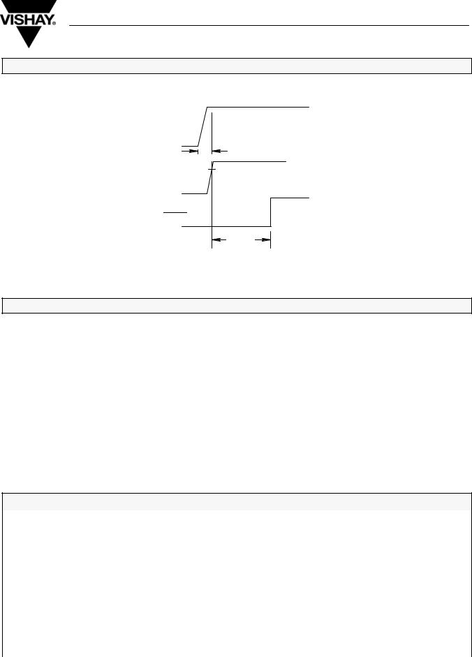
TIMING WAVEFORMS
VIN
tON
VNOM
0.95 VNOM
VOUT
ERROR
tDELAY
FIGURE 4. Timing Diagram for Power-Up
PIN CONFIGURATION
MSOP-8
CNOISE |
|
|
|
|
|
|
|
1 |
|
8 |
|
SD |
|
|
|
|
|
|
|
|
|
|
|
DELAY |
2 |
|
7 |
|
ERROR |
|
|
GND |
|
|
|
SENSE or ADJ |
|||
3 |
|
6 |
|||||
VIN |
|
|
|
|
VOUT |
||
4 |
|
5 |
|
||||
|
|
|
|
|
|
|
|
|
|
Top View |
|
|
|
|
|
PIN DESCRIPTION
Pin Number |
|
Name |
Function |
||||||
|
|
|
|
|
|
|
|
|
|
1 |
|
CNOISE |
Noise bypass pin. For low noise applications, a 0.01-mF or larger ceramic capacitor should be connected from this pin |
||||||
|
to ground. |
||||||||
|
|
|
|
|
|
Capacitor connected from this pin to ground will allow a delayed power-on-reset signal at the |
|
(Pin 7) output. |
|
2 |
|
DELAY |
ERROR |
||||||
|
Refer to Figure 4. |
||||||||
|
|
|
|
|
|
||||
|
|
|
|
|
|
|
|
||
3 |
|
GND |
Ground pin. Local ground for CNOISE and COUT. |
||||||
4 |
|
VIN |
Input supply pin. Bypass this pin with a 2.2-mF ceramic or tantalum capacitor to ground. |
||||||
5 |
|
VOUT |
Output voltage. Connect COUT between this pin and ground. |
||||||
6 |
SENSE or ADJ |
For fixed output voltage versions, this pin should be connected to VOUT (Pin 5). For adjustable output voltage version, |
|||||||
|
|
|
|
|
|
this voltage feedback pin sets the output voltage via an external resistor divider. |
|||
|
|
|
|
|
|
|
|
||
7 |
|
|
|
|
|
This open drain output is an error flag output which goes low when VOUT drops 5% below its nominal voltage. This pin |
|||
|
ERROR |
||||||||
|
|
|
|
|
|
also provides a power-on-reset signal if a capacitor is connected to the DELAY pin. |
|||
|
|
|
|
|
|
|
|||
8 |
|
|
|
|
By applying less than 0.4 V to this pin, the device will be turned off. Connect this pin to VIN if unused. |
||||
|
|
SD |
|||||||
|
|
|
|
|
|
|
|
|
|
www.vishay.com |
Document Number: 71150 |
4 |
S-50955—Rev. H, 16-May-05 |
 Loading...