


OPA381
OPA2381
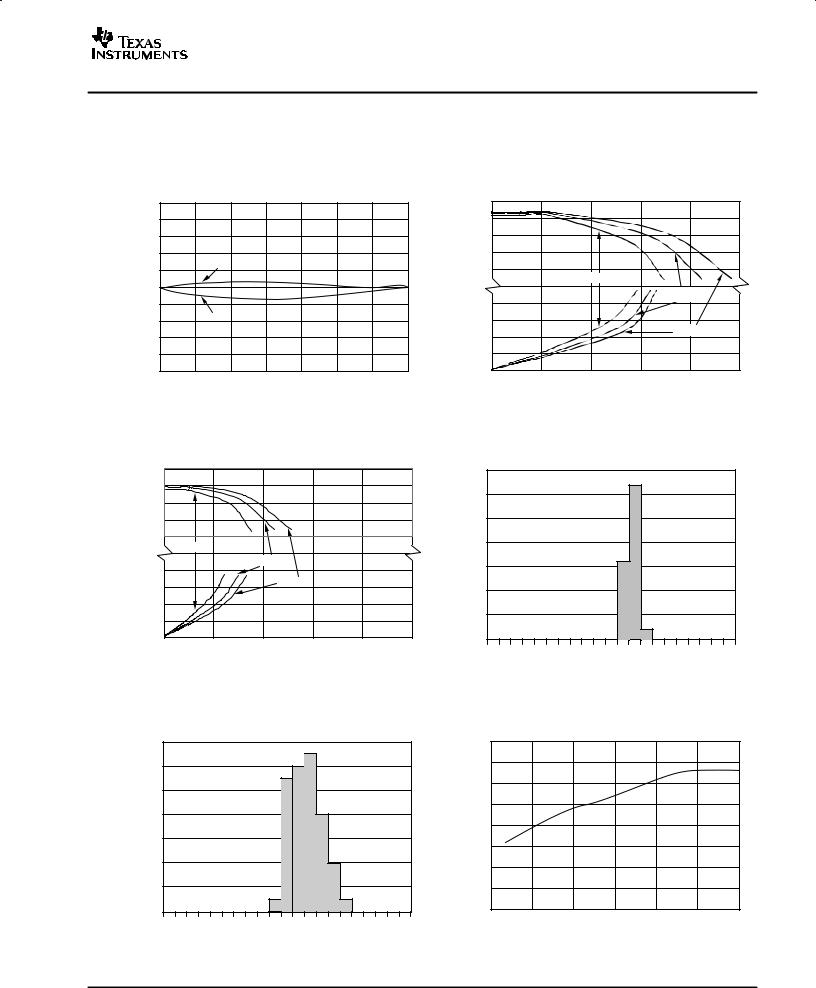
SBOS313B − AUGUST 2004 − REVISED NOVEMBER 2004
Precision, Low Power, 18MHz
Transimpedance Amplifier
FEATURES
DOVER 250kHz TRANSIMPEDANCE BANDWIDTH
DDYNAMIC RANGE: 5 Decades
DEXCELLENT LONG-TERM STABILITY
DLOW VOLTAGE NOISE: 10nV/√Hz
DBIAS CURRENT: 3pA
DOFFSET VOLTAGE: 25 V (max)
DOFFSET DRIFT: 0.1 V/°C (max)
DGAIN BANDWIDTH: 18MHz
DQUIESCENT CURRENT: 800 A
DFAST OVERLOAD RECOVERY
DSUPPLY RANGE: 2.7V to 5.5V
DSINGLE AND DUAL VERSIONS
DMicroPACKAGE: DFN-8, MSOP-8
APPLICATIONS
DPRECISION I/V CONVERSION
DPHOTODIODE MONITORING
DOPTICAL AMPLIFIERS
DCAT-SCANNER FRONT-END
DPHOTO LAB EQUIPMENT
|
RF |
|
|
|
|
+5V |
|
|
|
|
7 |
|
|
|
2 |
|
OPA381 |
|
VOUT |
|
|
|
||
|
|
|
6 |
(0V to 4.4V) |
|
|
|
|
|
CDIO DE |
|
|
|
R |
Photodiode |
|
|
|
P |
|
|
|
(Optional |
|
1MΩ |
65pF |
|
|
Pulldown |
|
|
Resistor) |
||
|
|
|
|
|
|
|
|
− 5V |
|
|
|
100kΩ |
|
|
3 |
|
|
|
|
|
|
75pF |
|
|
|
4 |
|
|
|
DESCRIPTION
The OPA381 family of transimpedance amplifiers provides 18MHz of Gain Bandwidth (GBW), with extremely high precision, excellent long-term stability, and very low 1/f noise. The OPA381 features an offset voltage of 25 V (max), offset drift of 0.1 V/°C (max), and bias current of 3pA. The OPA381 far exceeds the offset, drift, and noise performance that conventional JFET op amps provide.
The signal bandwidth of a transimpedance amplifier depends largely on the GBW of the amplifier and the parasitic capacitance of the photodiode, as well as the feedback resistor. The 18MHz GBW of the OPA381 enables a transimpedance bandwidth of > 250kHz in most configurations. The OPA381 is ideally suited for fast control loops for power level measurement on an optical fiber.
As a result of the high precision and low-noise characteristics of the OPA381, a dynamic range of 5 decades can be achieved. This capability allows the measurement of signal currents on the order of 10nA, and up to 1mA in a single I/V conversion stage. In contrast to logarithmic amplifiers, the OPA381 provides very wide bandwidth throughout the full dynamic range. By using an external pulldown resistor to –5V, the output voltage range can be extended to include 0V.
The OPA381 and OPA2381 are both available in MSOP-8 and DFN-8 (3mm x 3mm) packages. They are specified from –40°C to +125°C.
OPA381 RELATED DEVICES
PRODUCT |
FEATURES |
|
|
|
|
OPA380 |
90MHz GBW, 2.7V to 5.5V Supply |
|
Transimpedance Amplifier |
||
|
||
|
|
|
OPA132 |
16MHz GBW, Precision FET Op Amp ±15V |
|
|
|
|
OPA300 |
150MHz GBW, Low-Noise, 2.7V to 5.5V Supply |
|
|
|
|
OPA335 |
10 V VOS, Zero-Drift, 2.5V to 5V Supply |
|
OPA350 |
500 V VOS, 38MHz, 2.5V to 5V Supply |
|
OPA354 |
100MHz GBW CMOS, RRIO, 2.5V to 5V Supply |
|
|
|
|
OPA355 |
200MHz GBW CMOS, 2.5V to 5V Supply |
|
|
|
|
OPA656/7 |
230MHz, Precision FET, ±5V |
|
|
|
Please be aware that an important notice concerning availability, standard warranty, and use in critical applications of Texas Instruments semiconductor products and disclaimers thereto appears at the end of this data sheet.
All trademarks are the property of their respective owners.
PRODUCTION DATA information is current as of publication date. Products |
Copyright 2004, Texas Instruments Incorporated |
conform to specifications per the terms of Texas Instruments standard warranty. |
|
Production processing does not necessarily include testing of all parameters. |
|
www.ti.com

OPA381
OPA2381
www.ti.com
SBOS313B − AUGUST 2004 − REVISED NOVEMBER 2004
ABSOLUTE MAXIMUM RATINGS(1)
Voltage Supply . . . . . . . . . . . . . . . . . . . . . |
. . . . . . . |
. . . . . . . . . . . +7V |
Signal Input Terminals(2), Voltage . . . . . |
(V−) −0.5V to (V+) + 0.5V |
|
Current . . . . . . |
. . . . . . . |
. . . . . . . . ±10mA |
Short-Circuit Current(3) . . . . . . . . . . . . . . . . . . . . . . . . Continuous |
||
Operating Temperature Range . . . . . . . . |
. . . . . . . |
−40 °C to +125°C |
Storage Temperature Range . . . . . . . . . . |
. . . . . . . |
−65 °C to +150°C |
Junction Temperature . . . . . . . . . . . . . . . . |
. . . . . . . . |
. . . . . . . +150°C |
Lead Temperature (soldering, 10s) . . . . . . |
. . . . . . . . |
. . . . . . . +300°C |
OPA381 ESD Rating (Human Body Model) . . . . . . . |
. . . . . . . . 2000V |
|
OPA2381 ESD Rating (Human Body Model) . . . . . . |
. . . . . . . . 1500V |
|
(1)Stresses above these ratings may cause permanent damage. Exposure to absolute maximum conditions for extended periods may degrade device reliability. These are stress ratings only, and functional operation of the device at these or any other conditions beyond those specified is not implied.
(2)Input terminals are diode clamped to the power-supply rails. Input signals that can swing more than 0.5V beyond the supply rails should be current limited to 10mA or less.
(3)Short-circuit to ground; one amplifier per package.
PACKAGE/ORDERING INFORMATION(1)
ELECTROSTATIC DISCHARGE SENSITIVITY
This integrated circuit can be damaged by ESD. Texas
Instruments recommends that all integrated circuits be handled with appropriate precautions. Failure to observe
proper handling and installation procedures can cause damage.
ESD damage can range from subtle performance degradation to complete device failure. Precision integrated circuits may be more susceptible to damage because very small parametric changes could cause the device not to meet its published specifications.
|
|
PACKAGE |
SPECIFIED |
PACKAGE |
ORDERING |
TRANSPORT |
|
PRODUCT |
PACKAGE-LEAD |
TEMPERATURE |
|||||
DESIGNATOR |
MARKING |
NUMBER |
MEDIA, QUANTITY |
||||
|
|
RANGE |
|||||
|
|
|
|
|
|
||
|
|
|
|
|
|
|
|
OPA381 |
MSOP-8 |
DGK |
−40 °C to +125°C |
A64 |
OPA381AIDGKT |
Tape and Reel, 250 |
|
|
|
||||||
OPA381AIDGKR |
Tape and Reel, 2500 |
||||||
|
|
|
|
|
|||
|
|
|
|
|
|
|
|
OPA381 |
DFN-8 |
DRB |
−40 °C to +125°C |
A65 |
OPA381AIDRBT |
Tape and Reel, 250 |
|
|
|
||||||
OPA381AIDRBR |
Tape and Reel, 3000 |
||||||
|
|
|
|
|
|||
|
|
|
|
|
|
|
|
OPA2381 |
MSOP-8 |
DGK |
−40 °C to +125°C |
A62 |
OPA2381AIDGKT |
Tape and Reel, 250 |
|
|
|
||||||
OPA2381AIDGKR |
Tape and Reel, 2500 |
||||||
|
|
|
|
|
|||
|
|
|
|
|
|
|
|
OPA2381 |
DFN-8 |
DRB |
−40 °C to +125°C |
A63 |
OPA2381AIDRBT |
Tape and Reel, 250 |
|
|
|
||||||
OPA2381AIDRBR |
Tape and Reel, 3000 |
||||||
|
|
|
|
|
(1) For the most current package and ordering information, see the Package Option Addendum located at the end of this data sheet.
PIN ASSIGNMENTS |
|
|
|
|
|
|
|
|
Top View |
|
OPA381 |
|
|
|
OPA381 |
|
|
|
|
|
|
|
|
|
||
NC(1) |
1 |
8 |
NC(1) |
NC(1) |
1 |
Exposed |
8 |
NC(1) |
|
|
|
|
|
|
|
|
|
−In |
2 |
7 |
V+ |
−In |
2 |
Thermal |
7 |
V+ |
|
3 |
6 |
|
|
3 |
Die Pad |
6 |
|
+In |
Out |
+In |
on |
Out |
||||
V− 4 |
5 NC(1) |
V− 4 |
Underside |
5 NC(1) |
||||
|
||||||||
|
|
MSOP−8 |
|
|
|
DFN−8 |
|
|
|
|
|
|
NOTE: (1) NC indicates no internal connection. |
|
|
|
|
|
|
OPA2381 |
|
|
|
OPA2381 |
|
|
|
|
|
|
|
|
|
|
|
Out A |
1 |
8 |
V+ |
Out A |
1 |
Exposed |
8 |
V+ |
|
|
|
|
|
|
|
|
|
− In A |
2 |
7 |
Out B |
− In A |
2 |
Thermal |
7 |
Out B |
+In A |
3 |
6 |
− In B |
|
3 |
Die Pad |
6 |
− In B |
+In A |
on |
|||||||
V− |
4 |
5 |
+In B |
V− |
4 |
Underside |
5 |
+In B |
|
||||||||
|
|
MSOP−8 |
|
|
|
DFN−8 |
|
|
2

OPA381
OPA2381
www.ti.com
SBOS313B − AUGUST 2004 − REVISED NOVEMBER 2004
ELECTRICAL CHARACTERISTICS: VS = +2.7V to +5.5V
Boldface limits apply over the temperature range, TA = −40 °C to +125°C.
All specifications at TA = +25°C, RL = 10kΩ connected to VS/2, and VOUT = VS/2, unless otherwise noted.
|
|
|
|
|
|
|
OPA381 |
|
|
|
|
|
|
|
|
|
|
|
|
|
|
|
|
|
|
|
|
|
|
PARAMETER |
|
|
|
CONDITION |
MIN |
TYP |
|
MAX |
UNITS |
|||||
OFFSET VOLTAGE |
|
|
|
|
|
|
|
|
|
|
|
|
|
|
Input Offset Voltage |
VOS |
VS = +5V, VCM = 0V |
|
7 |
|
25 |
µV |
|||||||
Drift |
dVOS/dT |
|
|
|
|
|
0.03 |
|
0.1 |
µV/°C |
||||
vs Power Supply |
PSRR |
VS = +2.7V to +5.5V, VCM = 0V |
|
3.5 |
|
20 |
µV/V |
|||||||
Over Temperature |
|
VS = +2.7V to +5.5V, VCM = 0V |
|
|
|
20 |
µV/V |
|||||||
Long-Term Stability(1) |
|
|
|
|
|
|
See Note |
(1) |
µV/V |
|||||
Channel Separation, dc |
|
|
|
|
|
|
1 |
|
|
|||||
|
|
|
|
|
|
|
|
|
|
|
|
|
|
|
INPUT BIAS CURRENT |
|
|
|
|
|
|
|
|
|
|
|
|
|
|
Input Bias Current |
IB |
|
|
VCM = VS/2 |
|
3 |
|
±50 |
pA |
|||||
|
|
|
|
|||||||||||
Over Temperature |
|
|
|
|
|
See Typical Characteristics |
|
|
|
|
|
|||
Input Offset Current |
IOS |
|
|
VCM = VS/2 |
|
|
|
±100 |
pA |
|||||
|
|
|
6 |
|
||||||||||
NOISE |
|
|
|
|
|
|
|
|
|
|
|
|
|
|
Input Voltage Noise, f = 0.1Hz to 10Hz |
en |
VS = +5V, VCM = 0V |
|
3 |
|
|
µVPP |
|||||||
Input Voltage Noise Density, f = 10kHz |
en |
VS = +5V, VCM = 0V |
|
70 |
|
|
nV/√Hz |
|||||||
Input Voltage Noise Density, f > 1MHz |
en |
VS = +5V, VCM = 0V |
|
10 |
|
|
nV/√ |
Hz |
|
|||||
Input Current Noise Density, f = 10kHz |
in |
VS = +5V, VCM = 0V |
|
20 |
|
|
fA/√ |
Hz |
|
|||||
INPUT VOLTAGE RANGE |
|
|
|
|
|
|
|
|
|
|
|
|
|
|
Common-Mode Voltage Range |
VCM |
|
|
|
|
V− |
|
|
(V+) − 1.8V |
V |
||||
Common-Mode Rejection Ratio |
CMRR |
VS = +5V, (V−) < V CM < (V+) − 1.8V |
95 |
110 |
|
|
dB |
|||||||
INPUT IMPEDANCE |
|
|
|
|
|
|
|
|
|
|
|
|
|
|
Differential Capacitance |
|
|
|
|
|
|
1 |
|
|
pF |
||||
|
|
|
|
|
|
|
|
|||||||
Common-Mode Resistance and Capacitance |
|
|
|
|
|
|
1013|| 2.5 |
|
|
Ω || pF |
||||
|
|
|
|
|
|
|
|
|||||||
OPEN-LOOP GAIN |
|
|
|
|
|
|
|
|
|
|
|
|
|
|
Open-Loop Voltage Gain |
AOL |
0.05V < VO < (V+) − 0.6V, V CM = VS/2, VS = 5V |
110 |
135 |
|
|
dB |
|||||||
|
|
0V < VO < (V+) − 0.6V, V CM = 0V, RP = 10kΩ to −5V (2), VS = 5V |
106 |
135 |
|
|
dB |
|||||||
FREQUENCY RESPONSE |
|
|
|
|
|
|
|
|
|
|
|
|
|
|
Gain-Bandwidth Product |
GBW |
|
|
|
|
|
18 |
|
|
MHz |
||||
Slew Rate |
SR |
|
|
G = +1 |
|
|
12 |
|
|
V/µs |
||||
Settling Time, 0.0015%(3) |
|
V = +5V, 4V Step, G = +1, OPA381 |
|
7 |
|
|
µs |
|||||||
Settling Time, 0.003%(3) |
|
S |
|
|
|
|
|
|
|
µs |
||||
|
V = +5V, 4V Step, G = +1, OPA2381 |
|
7 |
|
|
|||||||||
Overload Recovery Time(4), (5) |
|
S |
V • G = > V |
|
|
200 |
|
|
ns |
|||||
|
|
S |
|
|
|
|||||||||
|
|
|
|
IN |
|
|
|
|
|
|
|
|
|
|
OUTPUT |
|
|
|
|
|
|
|
|
|
|
|
|
|
|
Voltage Output Swing from Positive Rail |
|
|
|
RL = 10kΩ |
|
|
400 |
|
600 |
mV |
||||
Voltage Output Swing from Negative Rail |
|
|
|
RL = 10kΩ |
|
|
30 |
|
50 |
mV |
||||
Voltage Output Swing from Positive Rail |
|
R |
P |
= 10kΩ to −5V (2) |
|
400 |
|
600 |
mV |
|||||
Voltage Output Swing from Negative Rail |
|
R |
= 10kΩ to −5V (2) |
|
−20 |
|
0 |
mV |
||||||
|
P |
|
|
|||||||||||
Output Current |
IOUT |
|
|
|
|
10 |
|
|
mA |
|||||
|
|
|
|
|
|
|
||||||||
Short-Circuit Current |
ISC |
|
|
|
|
|
20 |
|
|
mA |
||||
Capacitive Load Drive |
CLOAD |
|
|
|
|
See |
Typical Characteristics |
|
|
|
|
|
||
Open-Loop Output Impedance |
RO |
|
F = 1MHz, IO = 0 |
|
250 |
|
|
Ω |
||||||
|
|
|
|
|||||||||||
POWER SUPPLY |
|
|
|
|
|
|
|
|
|
|
|
|
|
|
Specified Voltage Range |
VS |
|
|
|
|
2.7 |
|
|
5.5 |
V |
||||
Quiescent Current (per amplifier) |
IQ |
|
|
IO = 0A |
|
|
0.8 |
|
1 |
mA |
||||
Over Temperature |
|
|
|
|
|
|
|
|
1.1 |
mA |
||||
|
|
|
|
|
|
|
|
|
|
|
|
|
|
|
TEMPERATURE RANGE |
|
|
|
|
|
|
|
|
|
|
|
|
|
|
Specified and Operating Range |
|
|
|
|
|
−40 |
|
|
+125 |
°C |
||||
Storage Range |
|
|
|
|
|
−65 |
|
|
+150 |
°C |
||||
Thermal Resistance |
qJA |
|
|
|
|
|
|
|
|
°C/W |
||||
MSOP-8 |
|
|
|
|
|
|
150 |
|
|
|||||
DFN-8 |
|
|
|
|
|
|
65 |
|
|
°C/W |
||||
(1)High temperature operating life characterization of zero-drift op amps applying the techniques used in the OPA381 have repeatedly demonstrated randomly distributed variation approximately equal to measurement repeatability of 1µV. This consistency gives confidence in the stability and repeatability of these zero-
drift techniques.
(2)Tested with output connected only to RP, a pulldown resistor connected between VOUT and −5V, as shown in Figure 3. See also Applications section, Achieving Output Swing to Negative Rail.
(3)Transimpedance frequency of 250kHz.
(4)Time required to return to linear operation.
(5)From positive rail.
3

OPA381
OPA2381
www.ti.com
SBOS313B − AUGUST 2004 − REVISED NOVEMBER 2004
TYPICAL CHARACTERISTICS: VS = +2.7V to +5.5V
All specifications at TA = +25°C, RL = 10kΩ connected to VS/2, and VOUT = VS/2, unless otherwise noted.
|
POWER−SUPPLY REJECTION RATIO AND |
OPEN−LOOP GAIN AND PHASE vs FREQUENCY |
COMMON−MODE REJECTION vs FREQUENCY |
|
140 |
|
|
|
|
|
|
200 |
|
140 |
|
|
|
|
|
|
|
|
120 |
|
|
|
Phase |
|
|
150 |
|
120 |
|
|
|
|
|
|
|
Open−LoopGain (dB) |
100 |
|
|
|
|
|
|
100 |
|
100 |
|
|
PSRR |
|
|
|
|
|
|
|
|
|
|
PSRR,CMRR (dB) |
80 |
|
|
|
|
|
|||||
20 |
|
|
|
|
|
|
−100Phase() |
|
|
|
CMRR |
|
|
|
|||
|
80 |
|
|
|
|
|
|
50 |
|
60 |
|
|
|
|
|
|
|
|
60 |
|
|
|
|
|
|
0 |
|
40 |
|
|
|
|
|
|
|
|
40 |
|
|
|
Gain |
|
|
−50 |
|
20 |
|
|
|
|
|
|
|
|
|
|
|
|
|
|
|
|
0 |
|
|
|
|
|
|
|
|
|
|
|
|
|
|
|
|
|
|
|
|
|
|
|
|
|
|
|
0 |
|
|
|
|
|
|
−150 |
|
−20 |
|
|
|
|
|
|
|
|
|
|
|
|
|
|
|
−40 |
|
|
|
|
|
|
|
||
|
|
|
|
|
|
|
|
|
|
|
|
|
|
|
|
|
|
|
−20 |
|
|
|
|
|
|
−200 |
|
−60 |
|
|
|
|
|
|
|
|
10 |
100 |
1k |
10k |
100k |
1M |
10M |
100M |
|
|
|
|
|
|
|
|
|
|
|
10 |
100 |
1k |
10k |
100k |
1M |
10M |
100M |
||||||||
|
|
|
|
Frequency (Hz) |
|
|
|
|
|
|
|
Frequency (Hz) |
|
|
|
||
|
|
|
PHASE MARGIN vs LOAD CAPACITANCE |
|
|
|
QUIESCENT CURRENT vs TEMPERATURE |
|
|||||||||
|
90 |
|
|
|
|
|
|
RS = 100Ω |
|
|
|
|
80 |
|
|
|
|
|
|
|
|
||
|
|
|
|
|
|
|
|
|
|
(mA) |
|
) |
70 |
|
|
|
|
|
|
|
100pF |
|
|
|
|
|
|
|
|
|
|
|
|
||
Margin( |
|
|
|
|
|
|
|
|
|
Current |
|
50 |
|
|
|
|
|
|
|
|
|
||
|
60 |
|
|
|
|
|
|
|
50kΩ |
|
|
|
|
|
|
|
|
|
|
|
|
RS |
|
Phase |
|
|
|
|
RS |
= 50Ω |
|
|
|
|
CL |
40 |
|
|
|
|
|
|
|
Quiescent |
|||
|
|
|
|
|
|
|
|
|
|||
|
|
|
|
|
|
|
|
|
|
|
|
|
30 |
|
|
|
|
|
RS = 0Ω |
|
|
|
|
|
20 |
|
|
|
|
|
|
|
|
||
|
|
|
|
|
|
|
|
|
|
|
|
|
10 |
|
|
|
|
|
|
|
|
|
|
|
0 |
100 |
200 |
300 |
400 |
500 |
600 |
700 |
800 |
900 |
1000 |
|
|
|
|
CL Load Capacitance (pF) |
|
|
|
||||
1.00
0.90
0.85
0.80
5.5V
0.75
0.70
0.65
2.7V
0.60
0.55
0.50
−40 − 25 |
0 |
25 |
50 |
75 |
100 |
125 |
|
|
Temperature (_C) |
|
|
|
|
QUIESCENT CURRENT vs SUPPLY VOLTAGE |
INPUT BIAS CURRENT vs TEMPERATURE |
|
1.00 |
|
|
|
|
|
|
|
|
0.90 |
|
|
|
|
|
|
|
(mA) |
0.85 |
|
|
|
|
|
|
(pA) |
0.80 |
|
|
|
|
|
|
||
Current |
|
|
|
|
|
|
Current |
|
0.75 |
|
|
|
|
|
|
||
|
|
|
|
|
|
|
|
|
Quiescent |
0.70 |
|
|
|
|
|
|
InputBias |
0.65 |
|
|
|
|
|
|
||
|
|
|
|
|
|
|
|
|
|
0.60 |
|
|
|
|
|
|
|
|
0.55 |
|
|
|
|
|
|
|
|
0.50 |
|
|
|
|
|
|
|
|
2.7 |
3.1 |
3.5 |
3.9 |
4.3 |
4.7 |
5.1 |
5.5 |
|
|
|
|
Supply Voltage (V) |
|
|
|
|
1000
100
10
1
−40 − 25 |
0 |
25 |
50 |
75 |
100 |
125 |
|
|
Temperature (_C) |
|
|
|
|
4
OPA381
OPA2381
www.ti.com
SBOS313B − AUGUST 2004 − REVISED NOVEMBER 2004
TYPICAL CHARACTERISTICS: VS = +2.7V to +5.5V (continued)
All specifications at TA = +25°C, RL = 10kΩ connected to VS/2, and VOUT = VS/2, unless otherwise noted.
Input Bias Current (pA)
|
|
INPUT BIAS CURRENT |
|
|
|
|
|
OUTPUT VOLTAGE SWING vs OUTPUT CURRENT |
|
||||||
50 |
|
vs COMMON−MODE VOLTAGE |
|
|
|
(V+) |
|
(VS = 5.5V) |
|
|
|||||
|
|
|
|
|
|
|
|
|
|
|
|
|
|||
40 |
|
|
|
|
|
|
|
|
|
|
|
|
|
|
|
30 |
|
|
|
|
|
|
|
|
(V+) − |
1 |
|
|
|
|
|
20 |
|
− IB |
|
|
|
|
|
(V) |
|
|
|
|
|
|
|
|
|
|
|
|
|
|
(V+) − |
|
|
|
|
|
|
||
0 |
|
|
|
|
|
|
Swing |
2 |
|
|
|
|
|
||
|
|
|
|
|
|
|
|
|
|
|
|
||||
10 |
|
|
|
|
|
|
|
|
|
+125_C |
|
|
|
||
|
|
|
|
|
|
|
|
|
|
|
|
|
|
|
|
−10 |
|
|
|
|
|
|
|
Output |
(V− ) + 2 |
|
|
|
+25°C |
|
|
|
+IB |
|
|
|
|
|
|
|
|
|
|
||||
|
|
|
|
|
|
|
|
|
|
|
|
||||
−20 |
|
|
|
|
|
|
|
|
|
|
|
|
|
|
|
|
|
|
|
|
|
|
|
|
|
|
|
|
−40_C |
|
|
−30 |
|
|
|
|
|
|
|
|
(V− ) + 1 |
|
|
|
|
||
|
|
|
|
|
|
|
|
|
|
|
|
|
|||
−40 |
|
|
|
|
|
|
|
|
|
|
|
|
|
|
|
−50 |
|
|
|
|
|
|
|
|
(V−) |
|
|
|
|
|
|
0 |
0.5 |
1.0 |
1.5 |
2.0 |
2.5 |
3.0 |
3.5 |
|
|
0 |
5 |
10 |
15 |
20 |
25 |
|
|
Common−Mode Voltage (V) |
|
|
|
|
|
|
Output Current (mA) |
|
|
||||
Output Swing (V)
|
OUTPUT VOLTAGE SWING vs OUTPUT CURRENT |
|
|
|
|
|
|
OFFSET VOLTAGE DRIFT |
|
|
|
|
|
|||
(V+) |
|
(VS = 2.7V) |
|
|
|
|
|
|
PRODUCTION DISTRIBUTION |
|
|
|
|
|
||
|
|
|
|
|
|
|
|
|
|
|
|
|
|
|
|
|
(V+) − 0.35 |
|
|
|
|
|
|
|
|
|
|
|
|
|
|
|
|
(V+) − 0.70 |
|
|
|
|
|
|
|
|
|
|
|
|
|
|
|
|
(V+) − 1.05 |
|
|
|
|
Population |
|
|
|
|
|
|
|
|
|
|
|
(V−) + 1.40 |
|
|
|
|
|
|
|
|
|
|
|
|
|
|
|
|
(V+) − 1.40 |
+125_C |
|
|
|
|
|
|
|
|
|
|
|
|
|
|
|
|
|
|
|
|
|
|
|
|
|
|
|
|
|
|
|
|
|
|
+25_C |
|
|
|
|
|
|
|
|
|
|
|
|
|
|
(V−) + 1.05 |
|
|
−40_C |
|
|
|
|
|
|
|
|
|
|
|
|
|
|
|
|
|
|
|
|
|
|
|
|
|
|
|
|
|
|
(V−) + 0.70 |
|
|
|
|
|
|
|
|
|
|
|
|
|
|
|
|
(V−) + 0.35 |
|
|
|
|
|
|
|
|
|
|
|
|
|
|
|
|
(V−) |
|
|
|
|
|
|
|
|
|
|
|
|
|
|
|
|
0 |
5 |
10 |
15 |
20 |
25 |
−0.09 |
−0.08 |
−0.07 |
−0.06 |
−0.05 |
−0.04 −0.03 −0.02 −0.01 0.00 0.01 0.02 0.03 0.04 0.05 |
|
|
|
|
|
|
|
Output Current (mA) |
|
−0.10 |
0.06 |
0.07 |
0.08 |
0.09 |
0.10 |
|||||||
|
|
|
|
|
|
|
|
|
|
|
Offset Voltage Drift (µV/_C) |
|
|
|
|
|
|
OFFSET VOLTAGE PRODUCTION DISTRIBUTION |
|
||||||||
Population |
|
|
|
|
|
|
|
|
|
Bandwidth (MHz) |
|
|
|
|
|
|
|
|
|
|
Gain |
−25.00 |
−20.00 |
−15.00 |
−10.00 |
−5.00 |
0.00 |
5.00 |
10.00 |
15.00 |
20.00 |
25.00 |
|
|
|
|
Offset Voltage (µV) |
|
|
|
|
||
GAIN BANDWIDTH vs POWER SUPPLY VOLTAGE
20
19
18
17
16
15
14
13
12
2.5 |
3.0 |
3.5 |
4.0 |
4.5 |
5.0 |
5.5 |
Power Supply Voltage (V)
5

OPA381
OPA2381
www.ti.com
SBOS313B − AUGUST 2004 − REVISED NOVEMBER 2004
TYPICAL CHARACTERISTICS: VS = +2.7V to +5.5V (continued)
All specifications at TA = +25°C, RL = 10kΩ connected to VS/2, and VOUT = VS/2, unless otherwise noted.
Circuit for Transimpedance Amplifier Characteristic curves on this page.
CF |
RF |
CSTRAY |
OPA381 |
CDIODE |
TRANSIMPEDANCE AMP CHARACTERISTIC
|
150 |
|
|
|
|
|
|
CDIODE = 50pF |
|
dB) |
140 |
|
|
|
|
|
|
|
|
130 |
RF = 10MΩ |
|
|
|
|
|
|
||
in |
120 |
|
|
|
|
|
|
||
|
|
|
|
|
|
|
|
||
(V/A |
110 |
R |
= 1MΩ |
CF = 1pF |
|
|
|
|
|
100 |
F |
|
|
|
|
|
|
|
|
Gain |
|
|
|
|
|
|
|
|
|
90 |
RF = 100kΩ |
|
CF = 3pF |
|
|
|
|
||
Transimpedance |
80 |
|
|
|
|
|
|
|
|
70 |
R |
= 10kΩ |
|
C |
= 8pF |
|
|
|
|
60 |
F |
|
|
F |
|
|
|
|
|
|
|
|
|
|
|
|
|
||
50 |
|
|
|
|
|
|
|
|
|
40 |
|
|
|
|
|
|
|
|
|
30 |
|
|
|
|
|
|
|
|
|
20 |
CSTRAY (parasitic) = 0.2pF |
|
|
|
|
||||
|
|
|
|
|
|||||
|
10 |
|
|
|
|
|
|
|
|
|
100 |
1k |
10k |
100k |
1M |
10M |
100M |
||
|
|
|
|
|
Frequency (Hz) |
|
|
|
|
TRANSIMPEDANCE AMP CHARACTERISTIC
|
150 |
|
|
|
|
|
CDIODE = 10pF |
|
dB) |
140 |
|
|
|
|
|
||
130 |
RF = 10MΩ |
|
|
|
|
|
||
in |
120 |
|
|
|
|
|
|
|
(V/A |
|
|
|
|
|
|
|
|
110 |
RF |
= 1MΩ |
CF |
= 0.5pF |
|
|
|
|
100 |
|
|
|
|
|
|||
Gain |
|
|
|
|
|
|
|
|
90 |
RF = 100kΩ |
|
CF = 2pF |
|
|
|
||
Transimpedance |
80 |
|
|
|
|
|
|
|
70 |
RF = 10kΩ |
|
|
|
|
|
||
60 |
|
|
|
CF = 4pF |
|
|
||
50 |
|
|
|
|
|
|||
40 |
|
|
|
|
|
|
|
|
30 |
CSTRAY (parasitic) = 0.2pF |
|
|
|
||||
20 |
|
|
|
|||||
|
|
|
|
|||||
|
10 |
|
|
|
|
|
|
|
|
100 |
1k |
10k |
100k |
1M |
10M |
100M |
|
Frequency (Hz)
TRANSIMPEDANCE AMP CHARACTERISTIC
|
150 |
|
|
|
|
|
CDIODE = 100pF |
|
dB) |
140 |
|
|
|
|
|
||
130 |
RF = 10MΩ |
CF = 0.5pF |
|
|
|
|
||
in |
120 |
|
|
|
|
|||
|
|
|
|
|
|
|
||
(V/A |
110 |
R |
= 1MΩ |
CF = 1pF |
|
|
|
|
100 |
F |
|
|
|
|
|
|
|
Gain |
|
|
|
|
|
|
|
|
90 |
RF = 100kΩ |
|
CF = 4pF |
|
|
|
||
Transimpedance |
80 |
|
|
|
|
|
|
|
70 |
R |
= 10kΩ |
|
C = 12pF |
|
|
|
|
60 |
F |
|
|
F |
|
|
|
|
|
|
|
|
|
|
|
||
50 |
|
|
|
|
|
|
|
|
40 |
|
|
|
|
|
|
|
|
30 |
|
|
|
|
|
|
|
|
20 |
CSTRAY (parasitic) = 0.2pF |
|
|
|
|
|||
|
|
|
|
|
||||
|
10 |
|
|
|
|
|
|
|
|
100 |
1k |
10k |
100k |
1M |
10M |
100M |
|
|
|
|
|
Frequency (Hz) |
|
|
|
|
TRANSIMPEDANCE AMP CHARACTERISTIC
|
150 |
|
|
|
|
|
CDIODE = 20pF |
|
dB) |
140 |
|
|
|
|
|
||
130 |
RF = 10MΩ |
|
|
|
|
|
||
in |
120 |
|
|
|
|
|
|
|
(V/A |
|
|
|
|
|
|
|
|
110 |
RF = 1MΩ |
CF = 0.5pF |
|
|
|
|||
Gain |
100 |
|
|
|
|
|
|
|
90 |
RF = 100kΩ |
|
C |
= 2pF |
|
|
||
Transimpedance |
80 |
|
|
|
F |
|
|
|
|
|
|
|
|
|
|
||
70 |
RF = 10kΩ |
|
|
|
|
|
||
60 |
|
|
|
CF = 5pF |
|
|
||
50 |
|
|
|
|
|
|
|
|
40 |
|
|
|
|
|
|
|
|
30 |
CSTRAY (parasitic) = 0.2pF |
|
|
|
||||
20 |
|
|
|
|||||
|
|
|
|
|||||
|
10 |
|
|
|
|
|
|
|
|
100 |
1k |
10k |
100k |
1M |
10M |
100M |
|
|
|
|
|
|
Frequency (Hz) |
|
|
|
TRANSIMPEDANCE AMP CHARACTERISTIC
|
150 |
|
|
|
|
|
CDIODE = 1pF |
|
dB) |
140 |
|
|
|
|
|
||
130 |
RF = 10MΩ |
|
|
|
|
|
||
in |
120 |
|
|
|
|
|
||
|
|
|
|
|
|
|
||
(V/A |
|
|
|
|
|
|
|
|
110 |
RF = 1MΩ |
|
|
|
|
|
||
100 |
|
|
|
|
|
|
|
|
Gain |
|
|
|
CF = 0.5pF |
|
|
|
|
90 |
RF = 100kΩ |
|
|
|
|
|||
|
|
|
|
|
||||
Transimpedance |
80 |
|
|
|
|
|
|
|
70 |
RF = 10kΩ |
|
|
CF = 2pF |
|
|||
60 |
|
|
|
|
|
|||
50 |
|
|
|
|
|
|
|
|
40 |
|
|
|
|
|
|
|
|
30 |
|
|
|
|
|
|
|
|
20 |
|
|
|
|
|
|
|
|
|
CSTRAY (parasitic) = 0.2pF |
|
|
|
|
|||
|
10 |
|
|
|
|
|||
|
|
|
|
|
|
|
|
|
|
100 |
1k |
10k |
100k |
1M |
10M |
100M |
|
Frequency (Hz)
6

OPA381
OPA2381
www.ti.com
SBOS313B − AUGUST 2004 − REVISED NOVEMBER 2004
TYPICAL CHARACTERISTICS: VS = +2.7V to +5.5V (continued)
All specifications at TA = +25°C, and RL = 10kΩ connected to VS/2, unless otherwise noted.
SMALL−SIGNAL STEP RESPONSE (with or without pull−down)
200kHz (CF = 16pF)
1MHz
 (CF = 3pF)
50mV/div |
CF |
50kΩ |
|
|
OPA381 |
10kΩ
VP VP = 0V or − 5V 
Time (100ns/div)
LARGE−SIGNAL STEP RESPONSE (without pull−down)
200kHz  1MHz (CF = 16pF)
 (CF = 3pF)
1V/div |
CF |
50kΩ |
|
|
OPA381 |
10kΩ
Time (100ns/div)
LARGE−SIGNAL STEP RESPONSE (with pull−down)
|
1V/div |
|
50kΩ |
|
|
|
|
3pF |
|
|
|
|
O PA3 81 |
|
|
|
|
10kΩ |
|
|
|
|
−5V |
|
|
|
|
Time (100ns/div) |
|
|
6 |
OVERLOAD RECOVERY |
|
|
|
VOUT |
|
40pF |
|
|
|
|
||
|
|
|
|
|
(V/div) |
|
|
|
20kΩ |
4 |
|
|
250µA |
|
|
|
|
||
|
|
|
|
|
OUT |
2 |
|
IIN |
OPA381 |
|
10kΩ |
|||
|
|
|
|
|
V |
|
Nonlinear |
Linear |
VP |
|
|
Operation |
Operation |
|
|
|
|
||
|
0 |
OPA381 |
|
|
(mA/div) |
|
|
|
|
0.8 |
OPA2381 |
|
|
|
|
|
|
||
|
|
|
VP = 0V or − 5V |
|
|
0 |
IIN |
|
|
IN |
|
|
|
|
I |
|
|
|
|
0 100 200 300 400 500 600 700 800 900 1000
Time (ns)
Input Voltage Noise (nV/√(Hz)
INPUT VOLTAGE NOISE SPECTRAL DENSITY
1000
100
10
1
10 |
100 |
1k |
10k |
100k |
1M |
10M |
|
|
|
Frequency (Hz) |
|
|
|
Channel Separation (dB)
CHANNEL SEPARATION vs INPUT FREQUENCY
160 


 OPA2381
140
120
100
80
60
40
20
0
−20
−40
10 |
100 |
1k |
10k |
100k |
1M |
10M |
100M |
Input Frequency (Hz)
7
 Loading...