


 Loading...
09/2005 Release 1.0
Service Repair Documentation
Level 4 (level 2,5e) – S75
Release |
Date |
Department |
Notes to change |
R 1.0 |
26.09.2005 |
BenQ MD CC GRM T |
New document |
|
|
|
|
|
|
|
|
Technical Documentation |
|
TD_Repair_L2.5_S75_R1.0.pdf |
Page 1 of 35 |

|
|
|
|
09/2005 |
|
|
|
|
Release 1.0 |
Table of Content |
|
|||
1 |
Introduction ............................................................................................................................... |
4 |
||
1.1 |
PURPOSE ............................................................................................................................... |
4 |
||
1.2 |
SCOPE ................................................................................................................................... |
4 |
||
1.3 |
TERMS AND ABBREVIATIONS ................................................................................................... |
4 |
||
2 |
List of available level 4 (level 2,5e) parts ............................................................................... |
5 |
||
3 |
Required Software for Level 4 (level 2,5e) .............................................................................. |
6 |
||
4 |
Radio Part .................................................................................................................................. |
7 |
||
4.1 |
BLOCK DIAGRAM RF PART....................................................................................................... |
8 |
||
4.2 |
POWER SUPPLY RF-PART ...................................................................................................... |
8 |
||
4.3 |
FREQUENCY GENERATION....................................................................................................... |
9 |
||
4.4 |
RECEIVER ............................................................................................................................ |
11 |
||
4.5 |
TRANSMITTER....................................................................................................................... |
12 |
||
4.6 |
BRIGHT IC OVERVIEW........................................................................................................... |
13 |
||
4.7 |
MECHANICAL ANTENNA SWITCH ............................................................................................ |
14 |
||
4.8 |
POWER AMPLIFIER AND POWER CONTROL............................................................................. |
15 |
||
5 |
Logic / Control ......................................................................................................................... |
16 |
||
5.1 |
OVERVIEW HARDWARE STRUCTURE S75............................................................................... |
16 |
||
5.2 |
SGOLD2 ............................................................................................................................. |
17 |
||
5.3 |
SDRAM............................................................................................................................... |
19 |
||
5.4 |
FLASH ................................................................................................................................ |
19 |
||
5.5 |
SIM...................................................................................................................................... |
|
19 |
|
5.6 |
VIBRATION MOTOR ............................................................................................................... |
20 |
||
6 |
Display...................................................................................................................................... |
|
20 |
|
7 |
ATI Gimmick ............................................................................................................................ |
20 |
||
8 |
Camera ..................................................................................................................................... |
|
20 |
|
9 |
Bluetooth.................................................................................................................................. |
21 |
||
10 |
Flashlight ................................................................................................................................. |
22 |
||
11 |
IRDA.......................................................................................................................................... |
|
22 |
|
12 |
Power Supply........................................................................................................................... |
22 |
||
12.1 |
ASIC MOZART / TWIGO4....................................................................................................... |
22 |
||
|
12.1.1 |
Battery....................................................................................................................... |
23 |
|
|
12.1.2 |
Charging Concept ..................................................................................................... |
23 |
|
|
|
|||
Technical Documentation |
|
|||
TD_Repair_L2.5_S75_R1.0.pdf |
Page 2 of 35 |
|||
|
|
|
|
|

|
|
|
09/2005 |
|
|
|
Release 1.0 |
12.2 |
EXTERNAL STEP-UP CONVERTER........................................................................................... |
25 |
|
13 |
Illumination .............................................................................................................................. |
26 |
|
14 |
Interfaces ................................................................................................................................. |
27 |
|
14.1 |
MICROPHONE (XG2001)....................................................................................................... |
27 |
|
14.2 |
BATTERY (X1400) ................................................................................................................ |
28 |
|
14.3 |
IRDA (V2650)...................................................................................................................... |
28 |
|
14.4 |
INTERFACE SIM MODULE WITH ESD PROTECTION ................................................................. |
29 |
|
14.5 |
IO CONNECTOR WITH ESD PROTECTION ............................................................................... |
30 |
|
14.6 |
VIBRATION MOTOR (XG2100)............................................................................................... |
31 |
|
14.7 |
BOARD TO BOARD CONNECTOR ............................................................................................ |
32 |
|
14.8 |
RSMMC READER................................................................................................................. |
33 |
|
14.9 |
CAMERA INTERFACE ............................................................................................................. |
34 |
|
14.10 |
DISPLAY CONNECTOR........................................................................................................ |
35 |
|
Technical Documentation |
|
TD_Repair_L2.5_S75_R1.0.pdf |
Page 3 of 35 |

09/2005 Release 1.0
1Introduction
1.1Purpose
This Service Repair Documentation is intended to carry out repairs on BenQ repair level 3-4.
1.2 Scope
This document is the reference document for all BenQ authorised Service Partners which are released to repair Siemens mobile phones up to level 2.5.
1.3 Terms and Abbreviations
Technical Documentation |
|
TD_Repair_L2.5_S75_R1.0.pdf |
Page 4 of 35 |
09/2005 Release 1.0
2 List of available level 4 |
(level 2,5e) parts |
||
(according to Component Matrix V1.09 - check C-market for updates) |
|||
Product |
ID |
Order Number |
Description CM |
S75 |
D1000 |
L50610-G6284-D670 |
IC SGOLD2 PMB8876 V2.1 |
S75 |
D1300 |
L50645-J4683-Y22 |
IC ASIC D1094ED-MOZART+ TWIGO4+ |
S75 |
D1301 |
L50610-B6189-D670 |
IC LOGIC 2 INPUT NAND NC7SP00L6X |
S75 |
D1302 |
L50610-B6186-D670 |
IC LOGIC 2 INPUT AND NC7SZ08L6X |
S75 |
D5100 |
L50610-U6122-D670 |
IC BLUETOOTH BRF6150 PB-FREE |
S75 |
D5400 |
L50610-L6156-D670 |
IC AUDIO VIDEO INTERFACE W2182 |
S75 |
L1301 |
L50651-F5103-M1 |
COIL 10U (Co-Type9) |
S75 |
L1302 |
L36151-F5103-M7 |
COIL 10U (Co-Type2) |
S75 |
N1330 |
L50620-C6258-D670 |
IC DC DC BOOST CONVERTER LM2733 |
S75 |
N3500 |
L506810-C6153-D670 |
IC ANA RE 2.9V USMD5 PB FREE |
S75 |
N3800 |
L36145-K280-Y258 |
IC FEM HITACHI GSM900 1800 1900 (Fem-Type1) |
S75 |
N3801 |
|
IC MODUL PA PF09026B (PA-Type4) |
S75 |
N3911 |
L50620-L6159-D670 |
IC TRANCEIVER HD155153NP |
S75 |
N4800 |
L506810-C6153-D670 |
IC ANA RE 2.9V USMD5 PB FREE |
S75 |
N5400 |
L50620-C6256-D670 |
IC ANA LM2770 |
S75 |
R3967 |
L36120-F4223-H |
RESISTOR TEMP 22K (Res-Type7) |
S75 |
V1302 |
L36840-D5076-D670 |
DIODE SOD323 (Di-Type7) |
S75 |
V1303 |
L36840-D5076-D670 |
DIODE SOD323 (Di-Type7) |
S75 |
V1305 |
L50630-C1107-D670 |
TRANSISTOR SI5933 (Tra-Type2) |
S75 |
V1400 |
L50640-D70-D670 |
DIODE BAV99T (Di-Type9) |
S75 |
V2100 |
L50640-D5084-D670 |
DIODE RB548W (Di-Type8) |
S75 |
V2302 |
L36840-C4014-D670 |
TRANSISTOR BC847BS BC846S (Tra-Type7) |
S75 |
V2330 |
L36840-C4014-D670 |
TRANSISTOR BC847BS BC846S (Tra-Type7) |
S75 |
V3961 |
L36840-D61-D670 |
DIODE 1SV305 (Di-Type4) |
S75 |
V3962 |
L36840-C2074-D670 |
IC DAC DAC3550A |
S75 |
V4901 |
L36840-C4014-D670 |
TRANSISTOR BC847BS BC846S (Tra-Type7) |
S75 |
V4903 |
L50630-C1138-D670 |
TRANSISTOR FDC633 (Tra-Type12) |
S75 |
V4904 |
L50630-C1138-D670 |
TRANSISTOR FDC633 (Tra-Type12) |
S75 |
Z1501 |
L50640-U6064-D670 |
FILTER EMI (Fi-Type6) PB Free |
S75 |
Z3961 |
L36145-F260-Y17 |
QUARZ 26MHZ (Q-Type4) |
S75 |
Z5100 |
L50645-K280-Y330 |
FILTER BP BLUETOOTH |
Technical Documentation |
|
TD_Repair_L2.5_S75_R1.0.pdf |
Page 5 of 35 |

09/2005 Release 1.0
Required Equipment for Level 4 (level 2,5e)
GSM-Tester (CMU200 or 4400S incl. Options)
PC-incl. Monitor, Keyboard and Mouse
Bootadapter 2000/2002 (L36880-N9241-A200)
Adapter cable for Bootadapter due to new Lumberg connector (F30032-P226-A1)
Troubleshooting Frame S75 (F30032-P533-A1)
Power Supply
Spectrum Analyser
Active RF-Probe incl. Power Supply
Oscilloscope incl. Probe
RF-Connector (N<>SMA(f))
Power Supply Cables
Dongle (F30032-P28-A1) if USB-Dongle is used a special driver for NT is required
BGA Soldering equipment
Reference: Equipment recommendation V1.6 (downloadable from the technical support page)
3Required Software for Level 4 (level 2,5e)
Windows XP
X-Focus version 1.68 or higher
GRT Version 3 or higher
Internet unblocking solution (JPICS)
Technical Documentation |
|
TD_Repair_L2.5_S75_R1.0.pdf |
Page 6 of 35 |

09/2005 Release 1.0
4 Radio Part
The radio part is realizes the conversion of the GMSK-HF-signals from the antenna to the baseband and vice versa.
In the receiving direction, the signals are split in the I- and Q-component and led to the D/A- converter of the logic part. In the transmission direction, the GMSK-signal is generated in an Up Conversion Modulation Phase Locked Loop by modulation of the I- and Q-signals which were generated in the logic part. After that the signals are amplified in the power amplifier.
Transmitter and Receiver are never active at the same time. Simultaneous receiving in the GSM850/EGSM900 and GSM1800/GSM1900 band is impossible. Simultaneous transmission in the GSM850/EGSM900 and GSM1800/GSM1900 band is impossible, too. However the monitoring band (monitoring timeslot) in the TDMA-frame can be chosen independently of the receiving respectively the transmitting band (RXand TX timeslot of the band).
S75 RF-part is dimensioned for triple band operation (EGSM900, DCS1800, PCS19000) supporting GPRS functionality up to multiclass 10.
The RF-circuit consists of the following components:
•Renesas Bright 5PL chip set (HD155153NP) with the following functionality:
PLL for local oscillator LO1 and LO2 and TxVCO
Integrated local oscillators LO1, LO2 (without loop filter)
Integrated TxVCO (without loop filter and core inductors for GSM)
Direct conversion receiver including LNA, DC-mixer, channel filtering and PGCamplifier
Active part of 26 MHz reference oscillator
Integrated Polar Loop, phase and amplitude control of transmitted output power
•Renesas LTCC transmit PA PF09026B (incl. integrated power control circuitry for GMSK mode)
•Frontend-Module including RX-/TX-switch and EGSM900 / DCS1800 / PCS 1900 receiver SAW-filters
•Crystal and passive circuitry of the 26MHz VCXO reference oscillator
Technical Documentation |
|
TD_Repair_L2.5_S75_R1.0.pdf |
Page 7 of 35 |

09/2005 Release 1.0
4.1 Block diagram RF part
4.2 Power Supply RF-Part
The voltage regulator for the RF-part is located inside the ASIC D1300. It generates the required 2,8V “RF-Voltages” named VDD_RF1 and VDD_RF2. VDD_RF2. The voltage regulator is activated as well as deactivated via VCXOEN_UC (Functional K19) provided by the SGOLD2. The temporary deactivation is used to extend the stand by time.
Technical Documentation |
|
TD_Repair_L2.5_S75_R1.0.pdf |
Page 8 of 35 |
09/2005 Release 1.0
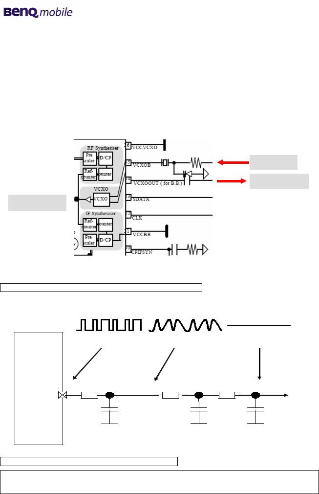
4.3 Frequency generation
The 26 MHz signal is created by a discrete VCXO (Z3961). The active part is realised within the Bright. For temperature measurements of the VCXO a temperature sensor (R3967) is used. The frequency of the reference oscillator can be fine tuned by the SGOLD2 via a filtered PNM modulated AFC signal (RF_AFC). Two active buffer stages are included in Bright 5PL to provide clock signals for the SGOLD2 and the Power Supply ASIC (BB_SIN26M). An additional external buffer (V3962) is used to deliver a 26MHz clock signal to the Bluetooth chip (BT_SIN26M).
VCXO Out
SGOLD2 In
Bright 5PL
The required voltage VDD_RF1 is provided by the ASIC D1300
S ig n alfo rm
S G O L D 2
1 |
2 |
3 |
1 |
R 1 |
A F C _ P N M |
2 |
R 2 |
R 3 |
3 |
|
|
|
|
|||
A F C |
|
|
|
|
|
|
|
|
C1 |
|
C2 |
|
C3 |
G N D G N D G N D
Waveform of the AFC signal from SGOLD2 to Oscillator
Technical Documentation |
|
TD_Repair_L2.5_S75_R1.0.pdf |
Page 9 of 35 |

09/2005 Release 1.0
Synthesizer: LO1
First local oscillator (LO1) consists of a PLL and VCO inside Bright (N3911) and an external loop filter (C3901, C3902).
RF PLL
The minimum frequency step is 400 kHz in GSM1800/GSM1900 mode and 800kHz in EGSM900 bands due to the internal divider by two for GSM1800/GSM1900 and divider by four for EGSM900. The PLL is controlled by the internal state machine which is connected to the SGOLD2 via tree-wire- bus.( RF_DAT; RF_CLK; RF_STR)
RFVCO (LO1)
The first local oscillator is needed to generate frequencies which enable the transceiver IC to demodulate the receiver signal and to perform the channel selection in the TX part. The full oscillation range is divided into 16 sub bands and covers 3476 to 3980MHz. To do so, a control voltage for the LO1 is used, gained by a comparator. This control voltage is a result of the comparison of the divided LO1 and the 26MHz reference Signal. The division ratio of the dividers is programmed by the SGOLD2, according to the network channel requirements.
Synthesizer: LO2
The second local oscillator (LO2) consists of a PLL and a VCO which are integrated in Bright 5PL (N3911)and a second order loopfilter which is realized external (C3940, C3941, R3952). Due to the direct conversion receiver architecture, the LO2 is only required for transmit operation in order to generate the transmit IF. To avoid inband spurious in the transmit signal the TX IF frequency is not fixed for the whole band. The LO2 covers a frequency range from 640 to 656MHz.
Before the LO2 signal enters the modulator it is divided by 8. So the resulting TX IF frequencies are 80/82 MHz. The complete LO2 operation is controlled by the Bright internal state machine.
he LO2 PLL and power-up of the VCO is controlled via the tree-wire-bus of Bright (SGOLD2 signals RF_DAT; RF_CLK; RF_STR). To ensure the frequency stability, the 640MHz VCO signal is compared by the phase detector of the 2nd PLL with the 26Mhz reference signal. The resulting control signal passes the external loop filter and is used to control the 640/656MHz VCO.
The required voltage VDD_RF1 is provided by the ASIC D1300
Frontend-Module (FEM)
The frontend module (N3800) includes the RX/TXand band-switch function based on a combined PIN diode and diplexer-circuit. In the transmit paths a harmonic filtering for EGSM900 and GSM1800/GSM1900 is realized to avoid additional discrete filters. The isolation in TX OFF mode is used to achieve the isolation which is necessary before the active part of the burst. Two lines from the SGOLD2 control the band-selection of the TX switches (RF_FE_CTRL_GSM, RF_FE_CTRL_GSM). The three receiver chains include SAW filter for EGSM900, GSM1800 and GSM1900 to protect the receivers from strong blocking signals.
Technical Documentation |
|
TD_Repair_L2.5_S75_R1.0.pdf |
Page 10 of 35 |
09/2005 Release 1.0
4.4 Receiver
Receiver: Filter to Demodulator
The Bright 5PL incorporates three RF LNAs for EGSM900, GSM1800 and GSM1900 operation followed by direct conversion mixers which are IQ demodulators. The LNA/mixer can be switched in normal-, lowand lower-gain mode. For the “normal gain“ state the mixers are optimised in terms of conversion gain and noise figure, in the “low gain“ state the mixers are optimised for large-signal behaviour for operation at a high input power levels. The "lower gain mode" reduces the RF-level by activating a differential impedance in front of the LNA to improve the large signal performance.
Furthermore the IC includes a programmable gain baseband amplifier PGA (90dB control range, 2dB steps) with automatic DC offset calibration. The channel filtering is realized inside the chip with a four stage baseband filter for both IQ chains. Only two capacitors which are part of the first passive RC-filters are external (C3905, C3906). The second, third and fourth filters are active filters and are fully integrated. The distributed channel filter is necessary to suppress adjacent channel and inband-blocking interferer to avoid any compression in each amplifier stage.
The downconverted IQ signals are fed into the A/D converters inside the SGOLD2. By a special algorithm the level of the IQ signals is kept constant on a defined level by varying the PGA gain and selecting the appropriate LNA gains.
Filter |
LNA |
Demodulator |
PGC |
N3800 |
|
Bright(N3911) |
|
The required voltage VDD_RF1 and VDD_RF2 are provided by the ASIC D1300
Technical Documentation |
|
TD_Repair_L2.5_S75_R1.0.pdf |
Page 11 of 35 |
Loading...