


Siemens SAB80C537-M, SAB80C537-M-T40-85, SAB80C537-M16, SAB80C537-N, SAB80C517-16-N-T40-85 Datasheet
...Microcomputer Components
8-Bit CMOS Single-Chip Microcontroller
SAB 80C517/80C537
Data Sheet 04.95
High-Performance |
SAB 80C517/80C537 |
8-Bit CMOS Single-Chip Microcontroller |
|
Advanced Information |
|
SAB 80C517 |
Microcontroller with factory mask-programmable ROM |
SAB 80C537 |
Microcontroller for external ROM |
●Versions for 12 MHz and 16 MHz operating frequency
●8 K × 8 ROM (SAB 80C517 only)
●256 × 8 on-chip RAM
●Superset of SAB 80C51 architecture:
1 μs instruction cycle time at 12 MHz
750 ns instruction cycle time at 16 MHz
256 directly addressable bits Boolean processor
64 Kbyte external data and program memory addressing
●Four 16-bit timer/counters
●Powerful 16-bit compare/capture unit (CCU) with up to 21 high-speed or PWM output channels and 5 capture inputs
●Versatile "fail-safe" provisions
●Fast 32-bit division, 16-bit 2 multiplication,
32-bit normalize and shift by peripheral
MUL/DIV unit (MDU)
●Eight data pointers for external memory addressing
●Fourteen interrupt vectors, four priority levels selectable
●8-bit A/D converter with 12 multiplexed inputs and programmable ref. voltages
●Two full duplex serial interfaces
●Fully upward compatible with SAB 80C515
●Extended power saving modes
●Nine ports: 56 I/O lines, 12 input lines
●Two temperature ranges available: 0 to 70 oC
– 40 to 85 oC
●Plastic packages: P-LCC-84,
P-MQFP-100-2
SAB 80C517/80C537 |
|
|
Semiconductor Group |
1 |
04.95 |

SAB 80C517/80C537
The SAB 80C517/80C537 is a high-end member of the Siemens SAB 8051 family of microcontrollers. It is designed in Siemens ACMOS technology and based on the SAB 8051 architecture. ACMOS is a technology which combines high-speed and density characteristics with low-power consumption or dissipation.
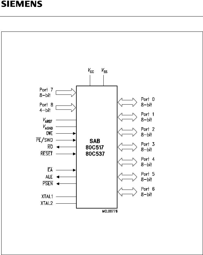
While maintaining all the SAB 80C515 features and operating characteristics the SAB 80C517 is expanded in its arithmetic capabilities, "fail-safe" characteristics, analog signal processing and timer capabilities. The SAB 80C537 is identical with the SAB 80C517 except that it lacks the on-chip program memory. The SAB 80C517/SAB 80C537 is supplied in a 84 pin plastic leaded chip carrier package (P-LCC-84) and in a 100-pin plastic quad metric flat package (P-MQFP-100-2).
Ordering Information
Type |
Ordering Code |
Package |
Description |
|
|
|
|
8-bit CMOS Microcontroller |
|
|
|
|
|
|
SAB 80C517-N |
Q67120-C397 |
P-LCC-84 |
with factory mask-programma- |
|
|
|
|
||
|
|
|
ble ROM, 12 MHz |
|
SAB 80C517-M |
TBD |
P-MQFP-100-2 |
||
|
|
|
|
|
SAB 80C537-N |
Q67120-C452 |
P-LCC-84 |
for external memory, 12 MHz |
|
|
|
|
||
SAB 80C537-M |
TBD |
P-MQFP-100-2 |
||
|
||||
|
|
|
|
|
SAB 80C517-N-T40/85 |
Q67120-C483 |
P-LCC-84 |
with factory mask-programma- |
|
|
|
|
ble ROM, 12 MHz, |
|
SAB 80C517-M-T40/85 |
TBD |
P-MQFP-100-2 |
||
ext. temperature – 40 to 85 °C |
||||
|
|
|
|
|
SAB 80C537-N-T40/85 |
Q67120-C484 |
P-LCC-84 |
for external ROM, 12 MHz, |
|
|
|
|
||
|
|
|
ext. temperature – 40 to 85 °C |
|
SAB 80C537-M-T40/85 |
TBD |
P-MQFP-100-2 |
||
|
|
|
|
|
SAB 80C517-N16 |
Q67120-C723 |
P-LCC-84 |
with mask-programmable |
|
|
|
|
ROM,16 MHz ext. temperature |
|
SAB 80C517-M16 |
TBD |
P-MQFP-100-2 |
||
– 40 to 110 °C |
||||
|
|
|
|
|
SAB 80C537-N16 |
Q67120-C722 |
P-LCC-84 |
for external memory, 16 MHz |
|
|
|
|
||
SAB 80C537-M16 |
TBD |
P-MQFP-100-2 |
||
|
||||
|
|
|
|
|
SAB 80C517-N16-T40/85 |
Q67120-C724 |
P-LCC-84 |
with mask-programmable ROM, |
|
|
|
|
16 MHz |
|
|
|
|
ext. temperature – 40 to 85 °C |
|
|
|
|
|
|
SAB 80C517-16-N-T40/85 |
Q67120-C725 |
P-LCC-84 |
with factory mask-programma- |
|
|
|
|
ble ROM, 12 MHz |
|
|
|
|
|
Semiconductor Group |
2 |
SAB 80C517/80C537
Logic Symbol
Semiconductor Group |
3 |
SAB 80C517/80C537
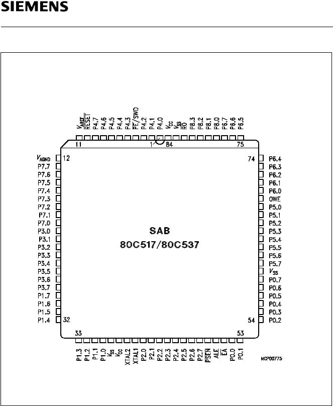
Pin Configuration
(P-LCC-84)
Semiconductor Group |
4 |
SAB 80C517/80C537
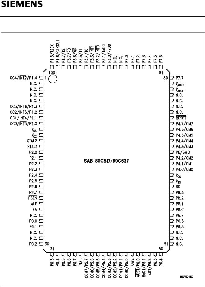
Pin Configuration |
|
(P-MQFP-100-2) |
|
Semiconductor Group |
5 |

SAB 80C517/80C537
Pin Definitions and Functions
Symbol |
Pin Number |
I/O *) |
|
Function |
|||
|
|
|
|
|
|
|
|
|
|
P-LCC-84 |
P-MQFP-100-2 |
|
|
|
|
|
|
|
|
|
|||
P4.0 – P4.7 |
1– 3, 5 – 9 |
64 - 66, |
I/O |
Port 4 |
|||
|
|
|
68 - 72 |
|
is a bidirectional I/O port with internal |
||
|
|
|
|
|
pull-up resistors. Port 4 pins that have |
||
|
|
|
|
|
1 s written to them are pulled high by |
||
|
|
|
|
|
the internal pull-up resistors, and in that |
||
|
|
|
|
|
state can be used as inputs. As inputs, |
||
|
|
|
|
|
port 4 pins being externally pulled low |
||
|
|
|
|
|
will source current (IIL, in the DC |
||
|
|
|
|
|
|
characteristics) because of the internal |
|
|
|
|
|
|
|
pull-up resistors. |
|
|
|
|
|
|
|
This port also serves alternate compare |
|
|
|
|
|
|
|
functions. The secondary functions are |
|
|
|
|
|
|
|
assigned to the pins of port 4 as |
|
|
|
|
|
|
|
follows: |
|
|
|
|
|
|
|
– CM0 (P4.0): Compare Channel 0 |
|
|
|
|
|
|
|
– CM1 (P4.1): Compare Channel 1 |
|
|
|
|
|
|
|
– CM2 (P4.2): Compare Channel 2 |
|
|
|
|
|
|
|
– CM3 (P4.3): Compare Channel 3 |
|
|
|
|
|
|
|
– CM4 (P4.4): Compare Channel 4 |
|
|
|
|
|
|
|
– CM5 (P4.5): Compare Channel 5 |
|
|
|
|
|
|
|
– CM6 (P4.6): Compare Channel 6 |
|
|
|
|
|
|
|
– CM7 (P4.7): Compare Channel 7 |
|
|
|
|
|
|
|
|
|
|
|
4 |
67 |
I |
|
|
|
PE/SWD |
Power saving modes enable/ |
||||||
|
|
|
|
|
|
Start Watchdog Timer |
|
|
|
|
|
|
|
A low level on this pin allows the |
|
|
|
|
|
|
|
software to enter the power down, idle |
|
|
|
|
|
|
|
and slow down mode. In case the low |
|
|
|
|
|
|
|
level is also seen during reset, the |
|
|
|
|
|
|
|
watchdog timer function is off on |
|
|
|
|
|
|
|
default. |
|
|
|
|
|
|
|
Use of the software controlled power |
|
|
|
|
|
|
|
saving modes is blocked, when this pin |
|
|
|
|
|
|
|
is held on high level. A high level during |
|
|
|
|
|
|
|
reset performs an automatic start of the |
|
|
|
|
|
|
|
watchdog timer immediately after reset. |
|
|
|
|
|
|
|
When left unconnected this pin is pulled |
|
|
|
|
|
|
|
high by a weak internal pull-up resistor. |
|
|
|
|
|
|
|
|
|
*I = Input
O = Output
Semiconductor Group |
6 |

SAB 80C517/80C537
Pin Definitions and Functions (cont’d)
Symbol |
Pin Number |
I/O *) |
|
Function |
|||
|
|
|
|
|
|
|
|
|
|
P-LCC-84 |
P-MQFP-100-2 |
|
|
|
|
|
|
|
|
|
|
|
|
|
|
10 |
73 |
I |
|
|
|
RESET |
|
|
RESET |
|
|||
|
|
|
|
|
|
A low level on this pin for the duration of |
|
|
|
|
|
|
|
one machine cycle while the oscillator is |
|
|
|
|
|
|
|
running resets the SAB 80C517. A small |
|
|
|
|
|
|
|
internal pull-up resistor permits |
|
|
|
|
|
|
|
power-on reset using only a capacitor |
|
|
|
|
|
|
|
connected to VSS. |
|
VAREF |
11 |
78 |
|
|
Reference voltage for the A/D con- |
||
|
|
|
|
|
|
verter. |
|
|
|
|
|
|
|
||
VAGND |
12 |
79 |
|
|
Reference ground for the A/D |
||
|
|
|
|
|
|
converter. |
|
|
|
|
|
|
|
||
P7.7 -P7.0 |
13 - 20 |
80 - 87 |
I |
|
Port 7 |
||
|
|
|
|
|
|
is an 8-bit unidirectional input port. Port |
|
|
|
|
|
|
|
pins can be used for digital input, if |
|
|
|
|
|
|
|
voltage levels meet the specified input |
|
|
|
|
|
|
|
high/low voltages, and for the lower |
|
|
|
|
|
|
|
8-bit of the multiplexed analog inputs of |
|
|
|
|
|
|
|
the A/D converter, simultaneously. |
|
|
|
|
|
|
|
|
|
* I = Input |
|
|
|
|
|
|
|
O = Output |
|
|
|
|
|
|
|
Semiconductor Group |
7 |

SAB 80C517/80C537
Pin Definitions and Functions (cont’d)
Symbol |
Pin Number |
I/O *) |
Function |
|||||||||||||
|
|
|
|
|
|
|
|
|
|
|
|
|
|
|
|
|
|
P-LCC-84 |
P-MQFP-100-2 |
|
|
|
|
|
|
|
|
|
|
|
|
|
|
|
|
|
|
|
||||||||||||
P3.0 - P3.7 |
21 - 28 |
90 - 97 |
I/O |
Port 3 |
||||||||||||
|
|
|
|
is a bidirectional I/O port with internal |
||||||||||||
|
|
|
|
pull-up resistors. Port 3 pins that have |
||||||||||||
|
|
|
|
1 s written to them are pulled high by |
||||||||||||
|
|
|
|
the internal pull-up resistors, and in that |
||||||||||||
|
|
|
|
state can be used as inputs. As inputs, |
||||||||||||
|
|
|
|
port 3 pins being externally pulled low |
||||||||||||
|
|
|
|
will source current (IIL, in the DC |
||||||||||||
|
|
|
|
characteristics) because of the internal |
||||||||||||
|
|
|
|
pull-up resistors. Port 3 also contains |
||||||||||||
|
|
|
|
the interrupt, timer, serial port 0 and |
||||||||||||
|
|
|
|
external memory strobe pins that are |
||||||||||||
|
|
|
|
used by various options. The output |
||||||||||||
|
|
|
|
latch corresponding to a secondary |
||||||||||||
|
|
|
|
function must be programmed to a one |
||||||||||||
|
|
|
|
(1) for that function to operate. |
||||||||||||
|
|
|
|
The secondary functions are assigned |
||||||||||||
|
|
|
|
to the pins of port 3, as follows: |
||||||||||||
|
|
|
|
– R × D0 (P3.0): receiver data input |
||||||||||||
|
|
|
|
|
(asynchronous) or data input/output |
|||||||||||
|
|
|
|
|
(synchronous) of serial interface |
|||||||||||
|
|
|
|
– T × D0 (P3.1): transmitter data |
||||||||||||
|
|
|
|
|
output (asynchronous) or clock |
|||||||||||
|
|
|
|
|
output (synchronous) of serial |
|||||||||||
|
|
|
|
|
interface 0 |
|||||||||||
|
|
|
|
|
|
|
|
|
|
|
|
|
|
|
|
|
|
|
|
|
– |
INT0 |
(P3.2): |
interrupt 0 input/timer 0 |
|||||||||
|
|
|
|
|
gate control |
|||||||||||
|
|
|
|
|
|
|
|
|
|
|
|
|
|
|
||
|
|
|
|
– |
INT1 |
(P3.3): |
interrupt 1 input/timer 1 |
|||||||||
|
|
|
|
|
gate control |
|||||||||||
|
|
|
|
– T0 (P3.4): counter 0 input |
||||||||||||
|
|
|
|
– T1 (P3.5): counter 1 input |
||||||||||||
|
|
|
|
– |
|
|
|
|
|
|
||||||
|
|
|
|
WR |
(P3.6): the |
write control signal |
|
|||||||||
|
|
|
|
|
latches the data byte from port 0 into |
|||||||||||
|
|
|
|
|
the external data memory |
|||||||||||
|
|
|
|
– |
|
|
|
|||||||||
|
|
|
|
RD |
(P3.7): the |
read control signal |
|
|||||||||
|
|
|
|
|
enables the external data |
|||||||||||
|
|
|
|
|
memory to port 0 |
|||||||||||
|
|
|
|
|
|
|
|
|
|
|
|
|
|
|
|
|
*I = Input
O = Output
Semiconductor Group |
8 |

SAB 80C517/80C537
Pin Definitions and Functions (cont’d)
Symbol |
Pin Number |
I/O *) |
Function |
||||||
|
|
|
|
|
|
|
|
|
|
|
P-LCC-84 |
P-MQFP-100-2 |
|
|
|
|
|
|
|
|
|
|
|
|
|||||
P1.7 - P1.0 |
29 - 36 |
98 - 100, |
I/O |
Port 1 |
|||||
|
|
1, 6 - 9 |
|
is a bidirectional I/O port with internal |
|||||
|
|
|
|
pull-up resistors. Port 1 pins that have |
|||||
|
|
|
|
1 s written to them are pulled high by |
|||||
|
|
|
|
the internal pull-up resistors, and in that |
|||||
|
|
|
|
state can be used as inputs. As inputs, |
|||||
|
|
|
|
port 1 pins being externally pulled low |
|||||
|
|
|
|
will source current (IIL, in the DC |
|||||
|
|
|
|
characteristics) because of the internal |
|||||
|
|
|
|
pull-up resistors. It is used for the low |
|||||
|
|
|
|
order address byte during program |
|||||
|
|
|
|
verifi-cation. It also contains the |
|||||
|
|
|
|
interrupt, timer, clock, capture and |
|||||
|
|
|
|
compare pins that are used by various |
|||||
|
|
|
|
options. The output latch must be |
|||||
|
|
|
|
programmed to a one (1) for that |
|||||
|
|
|
|
function to operate (except when used |
|||||
|
|
|
|
for the compare functions). |
|||||
|
|
|
|
The secondary functions are assigned |
|||||
|
|
|
|
to the port 1 pins as follows: |
|||||
|
|
|
|
|
|
|
|
|
|
|
|
|
|
– |
INT3/CC0 (P1.0): interrupt 3 input/ |
||||
|
|
|
|
|
compare 0 output / capture 0 input |
||||
|
|
|
|
– INT4/CC1 (P1.1): interrupt 4 input / |
|||||
|
|
|
|
|
compare 1 output /capture 1 input |
||||
|
|
|
|
– INT5/CC2 (P1.2): interrupt 5 input / |
|||||
|
|
|
|
|
compare 2 output /capture 2 input |
||||
|
|
|
|
– INT6/CC3 (P1.3): interrupt 6 input / |
|||||
|
|
|
|
|
compare 3 output /capture 3 input |
||||
|
|
|
|
|
|
|
|
|
|
|
|
|
|
– |
INT2/CC4 (P1.4): interrupt 2 input / |
||||
|
|
|
|
|
compare 4 output /capture 4 input |
||||
|
|
|
|
– T2EX (P1.5): timer 2 external reload |
|||||
|
|
|
|
|
trigger input |
||||
|
|
|
|
– |
CLKOUT (P1.6): system clock |
||||
|
|
|
|
|
output |
||||
|
|
|
|
– |
T2 (P1.7): counter 2 input |
||||
|
|
|
|
|
|
|
|
|
|
*I = Input
O = Output
Semiconductor Group |
9 |
SAB 80C517/80C537
Pin Definitions and Functions (cont’d)
Symbol |
Pin Number |
I/O *) |
Function |
|
|
|
|
|
|
|
P-LCC-84 |
P-MQFP-100-2 |
|
|
|
|
|
|
|
XTAL2 |
39 |
12 |
– |
XTAL2 |
|
|
|
|
Input to the inverting oscillator amplifier |
|
|
|
|
and input to the internal clock generator |
|
|
|
|
circuits. |
|
|
|
|
|
XTAL1 |
40 |
13 |
– |
XTAL1 |
|
|
|
|
Output of the inverting oscillator |
|
|
|
|
amplifier. To drive the device from an |
|
|
|
|
external clock source, XTAL2 should |
|
|
|
|
be driven, while XTAL1 is left |
|
|
|
|
unconnected. There are no |
|
|
|
|
requirements on the duty cycle of the |
|
|
|
|
external clock signal, since the input to |
|
|
|
|
the internal clocking circuitry is devided |
|
|
|
|
down by a divide-by-two flip-flop. |
|
|
|
|
Minimum and maximum high and low |
|
|
|
|
times as well as rise/fall times specified |
|
|
|
|
in the AC characteristics must be |
|
|
|
|
observed. |
|
|
|
|
|
P2.0 - P2.7 |
41 - 48 |
14 - 21 |
I/O |
Port 2 |
|
|
|
|
is a bidirectional I/O port with internal |
|
|
|
|
pull-up resistors. Port 2 pins that have |
|
|
|
|
1 s written to them are pulled high by |
|
|
|
|
the internal pull-up resistors, and in that |
|
|
|
|
state can be used as in-puts. As inputs, |
|
|
|
|
port 2 pins being externally pulled low |
|
|
|
|
will source current (IIL, in the DC |
|
|
|
|
characteristics) because of the internal |
|
|
|
|
pull-up resistors. Port 2 emits the high- |
|
|
|
|
order address byte during fetches from |
|
|
|
|
external program memory and during |
|
|
|
|
accesses to external data memory that |
|
|
|
|
use 16-bit addresses (MOVX @DPTR). |
|
|
|
|
In this application it uses strong |
|
|
|
|
internal pull-up resistors when issuing |
|
|
|
|
1 s. During accesses to external data |
|
|
|
|
memory that use 8-bit addresses |
|
|
|
|
(MOVX @Ri), port 2 issues the |
|
|
|
|
contents of the P2 special function |
|
|
|
|
register. |
|
|
|
|
|
*I = Input
O = Output
Semiconductor Group |
10 |

SAB 80C517/80C537
Pin Definitions and Functions (cont’d)
Symbol |
Pin Number |
I/O *) |
|
Function |
||||||
|
|
|
|
|
|
|
|
|
|
|
|
|
|
P-LCC-84 |
P-MQFP-100-2 |
|
|
|
|
|
|
|
|
|
|
|
|
|
|
|
|
|
|
|
|
49 |
22 |
O |
|
The |
|
|
|
PSEN |
|
|
Program Store Enable |
|||||||
|
|
|
|
|
|
|
output is a control signal that enables |
|||
|
|
|
|
|
|
|
the external program memory to the |
|||
|
|
|
|
|
|
|
bus during external fetch operations. It |
|||
|
|
|
|
|
|
|
is activated every six oscillator periodes |
|||
|
|
|
|
|
|
|
except during external data memory |
|||
|
|
|
|
|
|
|
accesses. Remains high during internal |
|||
|
|
|
|
|
|
|
pro-gram execution. |
|||
|
|
|
|
|
|
|||||
ALE |
50 |
23 |
O |
|
The Address Latch Enable |
|||||
|
|
|
|
|
|
|
output is used for latching the address |
|||
|
|
|
|
|
|
|
into external memory during normal |
|||
|
|
|
|
|
|
|
operation. It is activated every six |
|||
|
|
|
|
|
|
|
oscillator periodes except during an |
|||
|
|
|
|
|
|
|
external data memory access |
|||
|
|
|
|
|
|
|
||||
|
|
|
51 |
24 |
I |
|
|
|
|
|
EA |
|
|
External Access Enable |
|||||||
|
|
|
|
|
|
|
When held at high level, instructions |
|||
|
|
|
|
|
|
|
are fetched from the internal ROM |
|||
|
|
|
|
|
|
|
when the PC is less than 8192. When |
|||
|
|
|
|
|
|
|
held at low level, the SAB 80C517 |
|||
|
|
|
|
|
|
|
fetches all instructions from external |
|||
|
|
|
|
|
|
|
program memory. For the SAB 80C537 |
|||
|
|
|
|
|
|
|
this pin must be tied low |
|||
|
|
|
|
|
|
|||||
P0.0 - P0.7 |
52 - 59 |
26 - 27, |
I/O |
|
Port 0 |
|||||
|
|
|
|
30 - 35 |
|
|
is an 8-bit open-drain bidirectional I/O |
|||
|
|
|
|
|
|
|
port. Port 0 pins that have 1 s written to |
|||
|
|
|
|
|
|
|
them float, and in that state can be |
|||
|
|
|
|
|
|
|
used as high-impedance inputs. Port 0 |
|||
|
|
|
|
|
|
|
is also the multiplexed low-order |
|||
|
|
|
|
|
|
|
address and data bus during accesses |
|||
|
|
|
|
|
|
|
to external program or data memory. In |
|||
|
|
|
|
|
|
|
this application it uses strong internal |
|||
|
|
|
|
|
|
|
pull-up resistors when issuing 1 s. |
|||
|
|
|
|
|
|
|
Port 0 also outputs the code bytes |
|||
|
|
|
|
|
|
|
during program verification in the |
|||
|
|
|
|
|
|
|
SAB 83C517. External pull-up resistors |
|||
|
|
|
|
|
|
|
are required during program |
|||
|
|
|
|
|
|
|
verification. |
|||
|
|
|
|
|
|
|
|
|
|
|
*I = Input
O = Output
Semiconductor Group |
11 |

SAB 80C517/80C537
Pin Definitions and Functions (cont’d)
Symbol |
Pin Number |
I/O *) |
Function |
|
|
|
|
|
|
|
P-LCC-84 |
P-MQFP-100-2 |
|
|
|
|
|
|
|
P5.7 - P5.0 |
61 - 68 |
37 - 44 |
I/O |
Port 5 |
|
|
|
|
is a bidirectional I/O port with internal |
|
|
|
|
pull-up resistors. Port 5 pins that have |
|
|
|
|
1 s written to them are pulled high by |
|
|
|
|
the internal pull-up resistors, and in that |
|
|
|
|
state can be used as inputs. As inputs, |
|
|
|
|
port 5 pins being externally pulled low |
|
|
|
|
will source current (IIL, in the DC |
|
|
|
|
characteristics) because of the internal |
|
|
|
|
pull-up resistors. This port also serves |
|
|
|
|
the alternate function "Concurrent |
|
|
|
|
Compare". The secondary functions |
|
|
|
|
are assigned to the port 5 pins as |
|
|
|
|
follows: |
|
|
|
|
– CCM0 (P5.0): concurrent compare 0 |
|
|
|
|
– CCM1 (P5.1): concurrent compare 1 |
|
|
|
|
– CCM2 (P5.2): concurrent compare 2 |
|
|
|
|
– CCM3 (P5.3): concurrent compare 3 |
|
|
|
|
– CCM4(P5.4): concurrent compare 4 |
|
|
|
|
– CCM5 (P5.5): concurrent compare 5 |
|
|
|
|
– CCM6 (P5.6): concurrent compare 6 |
|
|
|
|
– CCM7(P5.7): concurrent compare 7 |
|
|
|
|
|
OWE |
69 |
45 |
I |
Oscillator Watchdog Enable |
|
|
|
|
A high level on this pin enables the |
|
|
|
|
oscillator watchdog. When left |
|
|
|
|
unconnected this pin is pulled high by a |
|
|
|
|
weak internal pull-up resistor. When |
|
|
|
|
held at low level the oscillator watchdog |
|
|
|
|
function is off. |
|
|
|
|
|
*I = Input
O = Output
Semiconductor Group |
12 |

SAB 80C517/80C537
Pin Definitions and Functions (cont’d)
Symbol |
Pin Number |
I/O *) |
Function |
|||
|
|
|
|
|
|
|
|
P-LCC-84 |
P-MQFP-100-2 |
|
|
|
|
|
|
|
|
|
||
P6.0 - P6.7 |
70 - 77 |
46 - 50, |
I/O |
Port 6 |
||
|
|
54 - 56 |
|
is a bidirectional I/O port with internal |
||
|
|
|
|
pull-up resistors. Port 6 pins that have |
||
|
|
|
|
1 s written to them are pulled high by |
||
|
|
|
|
the internal pull-up resistors, and in that |
||
|
|
|
|
state can be used as inputs. As inputs, |
||
|
|
|
|
port 6 pins being externally pulled low |
||
|
|
|
|
will source current (IIL, in the |
||
|
|
|
|
DC characteristics) because of the |
||
|
|
|
|
internal pull-up resistors. Port 6 also |
||
|
|
|
|
contains the external A/D converter |
||
|
|
|
|
control pin and the transmit and receive |
||
|
|
|
|
pins for serial channel 1. The output |
||
|
|
|
|
latch corresponding to a secondary |
||
|
|
|
|
function must be programmed to a one |
||
|
|
|
|
(1) for that function to operate. |
||
|
|
|
|
The secondary functions are assigned |
||
|
|
|
|
to the pins of port 6, as follows: |
||
|
|
|
|
|
||
|
|
|
|
– |
ADST |
(P6.0): external A/D converter |
|
|
|
|
|
start pin |
|
|
|
|
|
– R × D1 (P6.1): receiver data input of |
||
|
|
|
|
|
serial interface 1 |
|
|
|
|
|
– T × D1 (P6.2): transmitter data output |
||
|
|
|
|
of serial interface 1 |
||
|
|
|
|
|
||
P8.0 - P8.3 |
78 - 81 |
57 - 60 |
I |
Port 8 |
||
|
|
|
|
is a 4-bit unidirectional input port. Port |
||
|
|
|
|
pins can be used for digital input, if |
||
|
|
|
|
voltage levels meet the specified input |
||
|
|
|
|
high/low voltages, and for the higher |
||
|
|
|
|
4-bit of the multiplexed analog inputs of |
||
|
|
|
|
the A/D converter, simultaneously |
||
|
|
|
|
|
|
|
*I = Input
O = Output
Semiconductor Group |
13 |

SAB 80C517/80C537
Pin Definitions and Functions (cont’d)
Symbol |
Pin Number |
I/O *) |
|
Function |
||||
|
|
|
|
|
|
|
|
|
|
|
P-LCC-84 |
P-MQFP-100-2 |
|
|
|
|
|
|
|
|
|
|
|
|
|
|
|
|
82 |
61 |
|
O |
|
|
|
RO |
|
|
Reset Output |
|||||
|
|
|
|
|
|
|
This pin outputs the internally |
|
|
|
|
|
|
|
|
synchronized reset request signal. This |
|
|
|
|
|
|
|
|
signal may be generated by an external |
|
|
|
|
|
|
|
|
hardware reset, a watchdog timer reset |
|
|
|
|
|
|
|
|
or an oscillator watch-dog reset. The |
|
|
|
|
|
|
|
|
reset output is active low. |
|
|
|
|
|
|
|
|||
VSS |
37,60, 83 |
10, 62 |
– |
|
Circuit ground potential |
|||
VCC |
38,84 |
11, 63 |
– |
|
Supply Terminal for all operating |
|||
|
|
|
|
|
|
|
modes |
|
|
|
|
|
|
||||
N.C. |
– |
2 - 5, 25, |
– |
Not connected |
||||
|
|
|
28 |
- 29, |
|
|
|
|
|
|
|
36, |
|
|
|
|
|
|
|
|
51 |
- 53, |
|
|
|
|
|
|
|
74 |
- 77; |
|
|
|
|
|
|
|
88 |
- 89 |
|
|
|
|
|
|
|
|
|
|
|
|
|
*I = Input
O = Output
Semiconductor Group |
14 |

SAB 80C517/80C537
Figure 1
Block Diagram
Semiconductor Group |
15 |
SAB 80C517/80C537
Functional Description
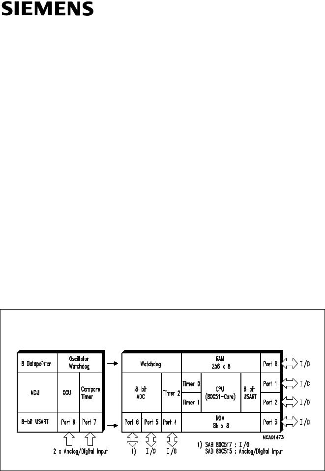
The SAB 80C517 is based on 8051 architecture. It is a fully compatible member of the Siemens SAB 8051/80C51 microcontroller family being a significantly enhanced SAB 80C515. The SAB 80C517 is therefore 100 % compatible with code written for the SAB 80C515.
CPU
Having an 8-bit CPU with extensive facilities for bit-handling and binary BCD arithmetics the SAB 80C517 is optimized for control applications. With a 12 MHz crystal, 58% of the instructions execute in 1 μs.
Being designed to close the performance gap to the 16-bit microcontroller world, the SAB 80C517’s CPU is supported by a powerful 32-/16-bit arithmetic unit and a more flexible addressing of external memory by eight 16-bit datapointers.
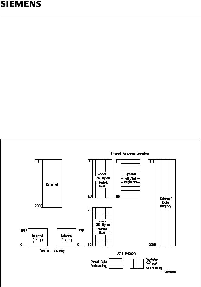
Memory Organisation
According to the SAB 8051 architecture, the SAB 80C517 has separate address spaces for program and data memory. Figure 2 illustrates the mapping of address spaces.
Figure 2
Memory Mapping
Semiconductor Group |
16 |

SAB 80C517/80C537
Program Memory
The SAB 80C517 has 8 KByte of on-chip ROM, while the SAB 80C537 has no internal ROM. The program memory can externally be expanded up to 64 Kbyte. Pin EA controls whether program fetches below address 2000H are done from internal or external memory.
Data Memory
The data memory space consists of an internal and an external memory space.
External Data Memory
Up to 64 KByte external data memory can be addressed by instructions that use 8-bit or 16-bit indirect addressing. For 8-bit addressing MOVX instructions utilizing registers R0 and R1 can be used. A 16-bit external memory addressing is supported by eight 16-bit datapointers.
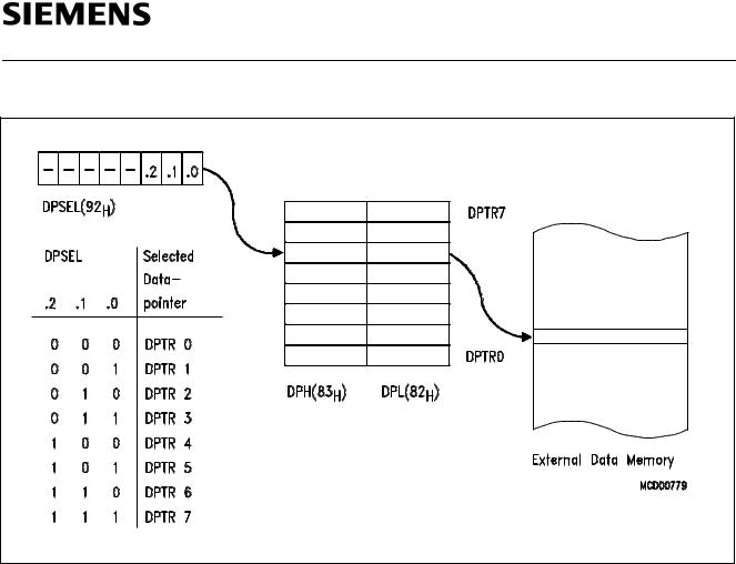
Multiple Datapointers
As a functional enhancement to standard 8051 controllers, the SAB 80C517 contains eight 16-bit datapointers. The instruction set uses just one of these datapointers at a time. The selection of the actual datapointers is done in special function register DPSEL (data pointer select, addr. 92H). Figure 3 illustrates the addressing mechanism.
Internal Data Memory
The internal data memory is divided into three physically distinct blocks:
–the lower 128 bytes of RAM including four banks of eight registers each
–the upper 128 byte of RAM
–the 128 byte special function register area.
A mapping of the internal data memory is also shown in figure 2. The overlapping address spaces are accessed by different addressing modes. The stack can be located anywhere in the internal data memory.
Semiconductor Group |
17 |
SAB 80C517/80C537
Figure 3
Addressing of External Data Memory
Semiconductor Group |
18 |
 Loading...