


C16x-Family of |
SAB 80C166W/ |
High-Performance CMOS 16-Bit Microcontrollers |
83C166W/ |
83C166W
Preliminary
SAB 80C166W/83C166W / 83C166W 16-Bit Microcontroller
●High Performance 16-bit CPU with 4-Stage Pipeline
●100 ns Instruction Cycle Time at 20 MHz CPU Clock
●500 ns Multiplication (16 × 16 bits), 1 μs Division (32 / 16 bit)
●Enhanced Boolean Bit Manipulation Facilities
●Register-Based Design with Multiple Variable Register Banks
●Single-Cycle Context Switching Support
●Up to 256 KBytes Linear Address Space for Code and Data
●1 KByte On-Chip RAM
●32 KBytes On-Chip ROM (SAB 83C166W only)
●Programmable External Bus Characteristics for Different Address Ranges
●8-Bit or 16-Bit External Data Bus
●Multiplexed or Demultiplexed External Address/Data Buses
●Hold and Hold-Acknowledge Bus Arbitration Support
●512 Bytes On-Chip Special Function Register Area
●Idle and Power Down Modes
●8-Channel Interrupt-Driven Single-Cycle Data Transfer Facilities via Peripheral Event Controller (PEC)
●16-Priority-Level Interrupt System
●10-Channel 10-bit A/D Converter with 9.7 μs Conversion Time
●16-Channel Capture/Compare Unit
●Two Multi-Functional General Purpose Timer Units with 5 Timers
●Two Serial Channels (USARTs)
●Programmable Watchdog Timer
●Up to 76 General Purpose I/O Lines
●Direct clock input without prescaler
●Supported by a Wealth of Development Tools like C-Compilers, Macro-Assembler Packages, Emulators, Evaluation Boards, HLL-Debuggers, Simulators, Logic Analyzer Disassemblers, Programming Boards
●On-Chip Bootstrap Loader
●100-Pin Plastic MQFP Package (EIAJ)
Semiconductor Group |
1 |
10.94 |
SAB 80C166W/83C166W
Introduction
The SAB 80C166W/83C166W is a representative of the Siemens SAB 80C166 family of full featured single-chip CMOS microcontrollers. It combines high CPU performance (up to 10 million instructions per second) with high peripheral functionality and enhanced IO-capabilities. These devices derive the CPU clock signal (operating clock) directly from the on-chip oscillator without using a prescaler. This reduces the device’s EME.
SAB 80C166W
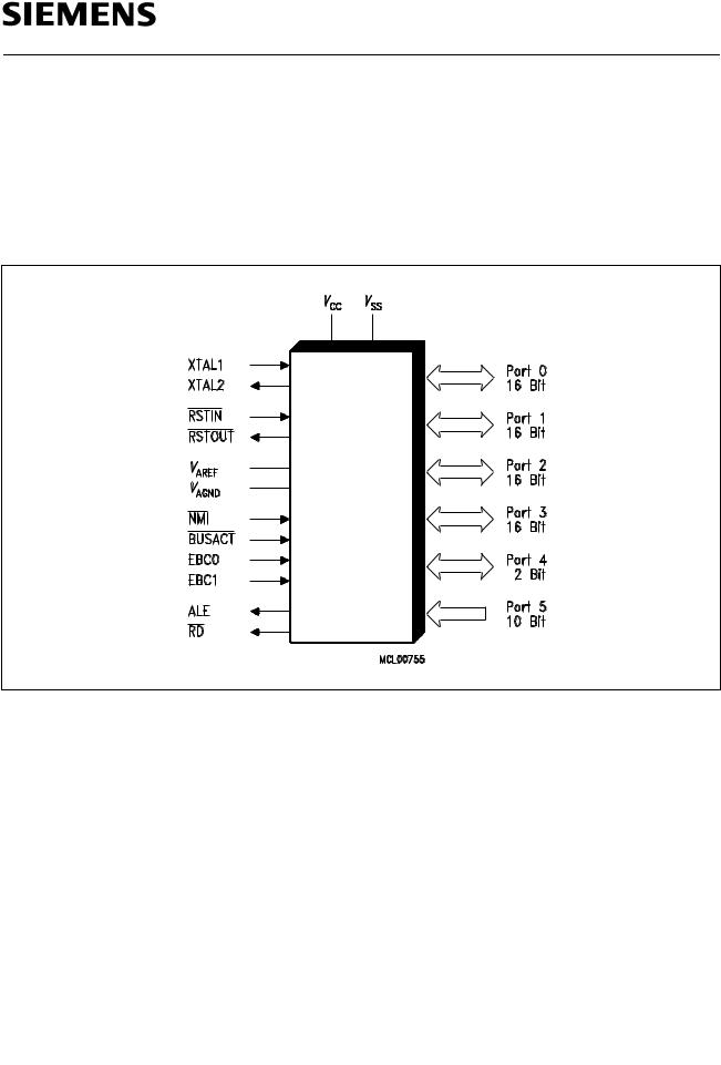
Figure 1
Logic Symbol
Ordering Information
Type |
Ordering Code |
Package |
Function |
|
|
|
|
SAB 83C166W-5M |
On Request |
P-MQFP-100-2 |
16-bit microcontroller, 0 ˚C to +70 ˚C, |
|
|
|
1 KByte RAM and 32 KByte ROM |
|
|
|
|
SAB 83C166W-5M- |
Q67120-D... |
P-MQFP-100-2 |
16-bit microcontroller, -40 ˚C to +85 ˚C, |
T3 |
|
|
1 KByte RAM and 32 KByte ROM |
|
|
|
|
SAB 83C166W-5M- |
Q67120-D... |
P-MQFP-100-2 |
16-bit microcontroller, -40 ˚C to +110 ˚C |
T4 |
|
|
1 KByte RAM and 32 KByte ROM |
|
|
|
|
SAB 80C166W/ |
On Request |
P-MQFP-100-2 |
16-bit microcontroller, 0 ˚C to +70 ˚C |
83C166W-M |
|
|
1 KByte RAM |
|
|
|
|
Semiconductor Group |
2 |
SAB 80C166W/83C166W
Type |
Ordering Code |
Package |
Function |
|
|
|
|
SAB 80C166W/ |
Q67120-C864 |
P-MQFP-100-2 |
16-bit microcontroller, -40 ˚C to +85 ˚C |
83C166W-M-T3 |
|
|
1 KByte RAM |
|
|
|
|
SAB 80C166W/ |
Q67120-C917 |
P-MQFP-100-2 |
16-bit microcontroller, -40 ˚C to +110 ˚C |
83C166W-M-T4 |
|
|
1 KByte RAM |
|
|
|
|
Note: The ordering codes (Q67120-D...) for the Mask-ROM versions are defined for each product after verification of the respective ROM code.
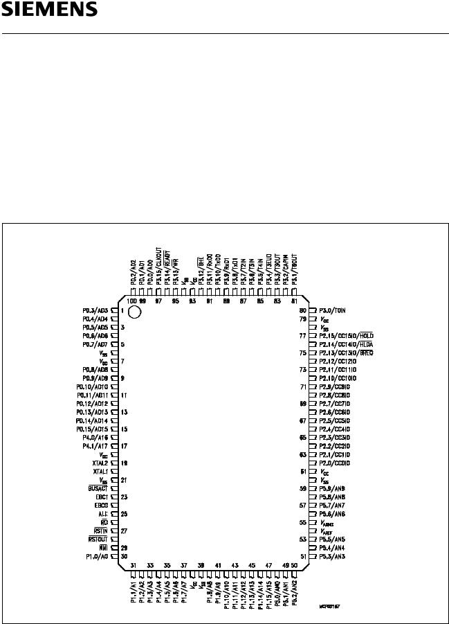
Pin Configuration Rectangular P-MQFP-100-2
(top view)
SAB 80C166W/
Figure 2
Semiconductor Group |
3 |

SAB 80C166W/83C166W
Pin Definitions and Functions
Pin |
|
Symbol |
Input (I) |
|
Function |
|
|
|
|
|
|
|
||||
No. |
|
|
|
|
|
Output (O) |
|
|
|
|
|
|
|
|
|
|
|
|
|
|
|
|
|
|
|||||||||
16 - 17 |
|
P4.0 – |
I/O |
|
Port 4 |
is a 2-bit |
bidirectional I/O port. It is bit-wise |
|||||||||
|
|
P4.1 |
|
|
programmable for input or output via direction bits. For a pin |
|||||||||||
|
|
|
|
|
|
|
|
configured as input, the output driver is put into high- |
||||||||
|
|
|
|
|
|
|
|
impedance state. |
|
|
|
|
|
|
||
|
|
|
|
|
|
|
|
In case of an external bus configuration, Port 4 can be used to |
||||||||
|
|
|
|
|
|
|
|
output the segment address lines: |
||||||||
16 |
|
|
|
|
|
O |
|
P4.0 |
A16 |
|
Least Significant Segment Addr. Line |
|||||
17 |
|
|
|
|
|
O |
|
P4.1 |
A17 |
|
Most Significant Segment Addr. Line |
|||||
|
|
|
|
|
|
|
||||||||||
20 |
|
XTAL1 |
I |
|
XTAL1: |
Input to the oscillator amplifier and input to the |
||||||||||
|
|
|
|
|
|
|
|
|
|
internal clock generator |
||||||
19 |
|
XTAL2 |
O |
|
XTAL2: |
Output of the oscillator amplifier circuit. |
||||||||||
|
|
|
|
|
|
|
|
To clock the device from an external source, drive XTAL1, |
||||||||
|
|
|
|
|
|
|
|
while leaving XTAL2 unconnected. Minimum and maximum |
||||||||
|
|
|
|
|
|
|
|
high/low and rise/fall times specified in the AC Characteristics |
||||||||
|
|
|
|
|
|
|
|
must be observed. |
|
|
|
|
|
|
||
|
|
|
|
|
|
|
||||||||||
22 |
|
|
|
|
|
I |
|
External Bus Configuration selection inputs. These pins are |
||||||||
|
BUSACT, |
|
|
|
||||||||||||
23 |
EBC1, |
I |
|
sampled during reset and select either the single chip mode or |
||||||||||||
24 |
EBC0 |
I |
|
one of the four external bus configurations: |
||||||||||||
|
|
|
|
|
|
|
|
|
EBC1 |
EBC0 Mode/Bus Configuration |
||||||
|
|
|
|
|
|
|
|
BUSACT |
|
|||||||
|
|
|
|
|
|
|
|
0 |
|
0 |
0 |
8-bit demultiplexed bus |
||||
|
|
|
|
|
|
|
|
0 |
|
0 |
1 |
8-bit multiplexed bus |
||||
|
|
|
|
|
|
|
|
0 |
|
1 |
0 |
16-bit muliplexed bus |
||||
|
|
|
|
|
|
|
|
0 |
|
1 |
1 |
16-bit demultiplexed bus |
||||
|
|
|
|
|
|
|
|
1 |
|
0 |
0 |
Single chip mode |
||||
|
|
|
|
|
|
|
|
1 |
|
0 |
1 |
Reserved. |
||||
|
|
|
|
|
|
|
|
1 |
|
1 |
0 |
Reserved. |
||||
|
|
|
|
|
|
|
|
1 |
|
1 |
1 |
Reserved. |
||||
|
|
|
|
|
|
|
|
|
|
|
||||||
|
|
|
|
|
|
|
|
ROMless versions must have pin |
BUSACT |
tied to ‘0’. |
||||||
|
|
|
|
|
|
|||||||||||
27 |
|
|
|
|
|
I |
|
Reset Input with Schmitt-Trigger characteristics. A low level |
||||||||
|
RSTIN |
|
|
|
||||||||||||
|
|
|
|
|
|
|
|
at this pin for a specified duration while the oscillator is running |
||||||||
|
|
|
|
|
|
|
|
resets the SAB 80C166W/83C166W. An internal pullup |
||||||||
|
|
|
|
|
|
|
|
resistor permits power-on reset using only a capacitor |
||||||||
|
|
|
|
|
|
|
|
connected to VSS. |
|
|
|
|
|
|
||
|
|
|
|
|
||||||||||||
28 |
|
|
|
|
|
O |
|
Internal Reset Indication Output. This pin is set to a low |
||||||||
|
RSTOUT |
|
|
|||||||||||||
|
|
|
|
|
|
|
|
level when the part is executing either a hardware-, a |
||||||||
|
|
|
|
|
|
|
|
softwareor a watchdog timer reset. |
RSTOUT |
remains low |
||||||
|
|
|
|
|
|
|
|
until the EINIT (end of initialization) instruction is executed. |
||||||||
|
|
|
|
|
|
|
|
|
|
|
|
|
|
|
|
|
Semiconductor Group |
4 |

SAB 80C166W/83C166W
Pin Definitions and Functions (cont’d)
Pin |
|
Symbol |
Input (I) |
Function |
|
|
|
|
|
|
|
|
|
|
|
|
||
No. |
|
|
|
|
Output (O) |
|
|
|
|
|
|
|
|
|
|
|
|
|
|
|
|
|
|
||||||||||||||
29 |
|
|
|
|
I |
Non-Maskable Interrupt Input. A high to low transition at this |
||||||||||||
|
NMI |
|
||||||||||||||||
|
|
|
|
|
|
pin causes the CPU to vector to the NMI trap routine. When |
||||||||||||
|
|
|
|
|
|
|
|
|
|
|
|
|
|
|
||||
|
|
|
|
|
|
the PWRDN (power down) instruction is executed, the |
NMI |
pin |
||||||||||
|
|
|
|
|
|
must be low in order to force the SAB 80C166W/83C166W to |
||||||||||||
|
|
|
|
|
|
go into power down mode. If |
NMI |
|
is high, when PWRDN is |
|||||||||
|
|
|
|
|
|
executed, the part will continue to run in normal mode. |
||||||||||||
|
|
|
|
|
|
If not used, pull |
NMI |
high externally. |
||||||||||
|
|
|
|
|
||||||||||||||
29 |
|
ALE |
O |
Address Latch Enable Output. Can be used for latching the |
||||||||||||||
|
|
|
|
|
|
address into external memory or an address latch in the |
||||||||||||
|
|
|
|
|
|
multiplexed bus modes. |
||||||||||||
|
|
|
|
|
|
|||||||||||||
26 |
|
|
|
|
O |
External Memory Read Strobe. |
|
is activated for every |
||||||||||
|
RD |
|
RD |
|||||||||||||||
|
|
|
|
|
|
external instruction or data read access. |
||||||||||||
|
|
|
|
|||||||||||||||
30 - 37 |
P1.0 – |
I/O |
Port 1 is a 16-bit bidirectional I/O port. It is bit-wise |
|||||||||||||||
40 - 47 |
P1.15 |
|
programmable for input or output via direction bits. For a pin |
|||||||||||||||
|
|
|
|
|
|
configured as input, the output driver is put into high- |
||||||||||||
|
|
|
|
|
|
impedance state. Port 1 is used as the 16-bit address bus (A) |
||||||||||||
|
|
|
|
|
|
in demultiplexed bus modes and also after switching from a |
||||||||||||
|
|
|
|
|
|
demultiplexed bus mode to a multiplexed bus mode.. |
||||||||||||
|
|
|
|
|||||||||||||||
48 - 53 |
P5.0 – |
I |
Port 5 is a 10-bit input-only port with Schmitt-Trigger |
|||||||||||||||
56 - 59 |
P5.9 |
I |
characteristics. The pins of Port 5 also serve as the (up to 10) |
|||||||||||||||
|
|
|
|
|
|
analog input channels for the A/D converter, where P5.x |
||||||||||||
|
|
|
|
|
|
equals ANx (Analog input channel x). |
||||||||||||
|
|
|
|
|||||||||||||||
62 - 77 |
P2.0 – |
I/O |
Port 2 is a 16-bit bidirectional I/O port. It is bit-wise |
|||||||||||||||
|
P2.15 |
|
programmable for input or output via direction bits. For a pin |
|||||||||||||||
|
|
|
|
|
|
configured as input, the output driver is put into high- |
||||||||||||
|
|
|
|
|
|
impedance state. |
|
|
|
|
|
|
|
|||||
|
|
|
|
|
|
The following Port 2 pins also serve for alternate functions: |
||||||||||||
62 |
|
|
|
|
I/O |
P2.0 |
CC0IO |
CAPCOM: CC0 Cap.-In/Comp.Out |
||||||||||
|
|
|
|
|
|
... |
... |
|
|
|
|
... |
|
|
|
|
|
|
75 |
|
|
|
|
I/O |
P2.13 |
CC13IO |
CAPCOM: CC13 Cap.-In/Comp.Out, |
||||||||||
|
|
|
|
|
O |
|
BREQ |
|
External Bus Request Output |
|||||||||
76 |
|
|
|
|
I/O |
P2.14 |
CC14IO |
CAPCOM: CC14 Cap.-In/Comp.Out, |
||||||||||
|
|
|
|
|
O |
|
|
|
External Bus Hold Acknowl. Output |
|||||||||
|
|
|
|
|
|
HLDA |
|
|
||||||||||
77 |
|
|
|
|
I/O |
P2.15 |
CC15IO |
CAPCOM: CC15 Cap.-In/Comp.Out, |
||||||||||
|
|
|
|
|
I |
|
|
External Bus Hold Request Input |
||||||||||
|
|
|
|
|
|
HOLD |
|
|||||||||||
|
|
|
|
|
|
|
|
|
|
|
|
|
|
|
|
|
|
|
Semiconductor Group |
5 |

SAB 80C166W/83C166W
Pin Definitions and Functions (cont’d)
Pin |
Symbol |
Input (I) |
Function |
|
|
|
|
|
|
||
No. |
|
Output (O) |
|
|
|
|
|
|
|
|
|
|
|
|
|
|
|
|
|||||
80 |
- 92, |
P3.0 – |
I/O |
Port 3 is a 16-bit |
bidirectional |
I/O port. It is bit-wise |
|||||
95 |
- 97 |
P3.15 |
I/O |
programmable for input or output via direction bits. For a pin |
|||||||
|
|
|
|
configured as input, the output driver is put into high- |
|||||||
|
|
|
|
impedance state. |
|
|
|||||
|
|
|
|
The following Port 3 pins also serve for alternate functions: |
|||||||
80 |
|
|
I |
P3.0 |
|
T0IN |
CAPCOM Timer T0 Count Input |
||||
81 |
|
|
O |
P3.1 |
|
T6OUT |
GPT2 Timer T6 Toggle Latch Output |
||||
82 |
|
|
I |
P3.2 |
|
CAPIN |
GPT2 Register CAPREL Capture Input |
||||
83 |
|
|
O |
P3.3 |
|
T3OUT |
GPT1 Timer T3 Toggle Latch Output |
||||
84 |
|
|
I |
P3.4 |
|
T3EUD |
GPT1 Timer T3 Ext.Up/Down Ctrl.Input |
||||
85 |
|
|
I |
P3.5 |
|
T4IN |
GPT1 Timer T4 Input for |
||||
|
|
|
|
|
|
|
|
|
|
Count/Gate/Reload/Capture |
|
86 |
|
|
I |
P3.6 |
|
T3IN |
GPT1 Timer T3 Count/Gate Input |
||||
87 |
|
|
I |
P3.7 |
|
T2IN |
GPT1 Timer T2 Input for |
||||
|
|
|
|
|
|
|
|
|
|
Count/Gate/Reload/Capture |
|
88 |
|
|
O |
P3.8 |
|
TxD1 |
ASC1 Clock/Data Output (Asyn./Syn.) |
||||
89 |
|
|
I/O |
P3.9 |
|
RxD1 |
ASC1 Data Input (Asyn.) or I/O (Syn.) |
||||
90 |
|
|
O |
P3.10 |
T×D0 |
ASC0 Clock/Data Output (Asyn./Syn.) |
|||||
91 |
|
|
I/O |
P3.11 |
R×D0 |
ASC0 Data Input (Asyn.) or I/O (Syn.) |
|||||
92 |
|
|
O |
P3.12 |
BHE |
|
|
Ext. Memory High Byte Enable Signal, |
|||
95 |
|
|
O |
P3.13 |
WR |
|
|
External Memory Write Strobe |
|||
96 |
|
|
I |
P3.14 |
READY |
|
Ready Signal Input |
||||
97 |
|
|
O |
P3.15 |
CLKOUT |
System Clock Output (=CPU Clock) |
|||||
|
|
|
|
|
|||||||
98 |
– 5 |
P0.0 – |
I/O |
Port 0 is a 16-bit bidirectional IO port. It is bit-wise |
|||||||
8 – 15 |
P0.15 |
|
programmable for input or output via direction bits. For a pin |
||||||||
|
|
|
|
configured as input, the output driver is put into high- |
|||||||
|
|
|
|
impedance state. |
|
|
|||||
|
|
|
|
In case of an external bus configuration, Port 0 serves as the |
|||||||
|
|
|
|
address (A) and address/data (AD) bus in multiplexed bus |
|||||||
|
|
|
|
modes and as the data (D) bus in demultiplexed bus modes. |
|||||||
|
|
|
|
Demultiplexed bus modes: |
|
||||||
|
|
|
|
Data Path Width: |
8-bit |
16-bit |
|||||
|
|
|
|
P0.0 |
– P0.7: |
D0 – D7 |
D0 - D7 |
||||
|
|
|
|
P0.8 |
– P0.15: |
output! |
D8 - D15 |
||||
|
|
|
|
Multiplexed bus modes: |
|
||||||
|
|
|
|
Data Path Width: |
8-bit |
16-bit |
|||||
|
|
|
|
P0.0 |
– P0.7: |
AD0 – AD7 |
AD0 - AD7 |
||||
|
|
|
|
P0.8 |
– P0.15: |
A8 - A15 |
AD8 - AD15 |
||||
|
|
|
|
|
|||||||
54 |
|
VAREF |
- |
Reference voltage for the A/D converter. |
|||||||
55 |
|
VAGND |
- |
Reference ground for the A/D converter. |
|||||||
Semiconductor Group |
6 |

SAB 80C166W/83C166W
Pin Definitions and Functions (cont’d)
Pin |
Symbol |
Input (I) |
Function |
No. |
|
Output (O) |
|
|
|
|
|
7, 18, |
VCC |
- |
Digital Supply Voltage: |
38, 61, |
|
|
+ 5 V during normal operation and idle mode. |
79, 93 |
|
|
³ 2.5 V during power down mode |
|
|
|
|
6, 21, |
VSS |
- |
Digital Ground. |
39, 60, |
|
|
|
78, 94 |
|
|
|
|
|
|
|
Semiconductor Group |
7 |

SAB 80C166W/83C166W
Functional Description
The architecture of the SAB 80C166W/83C166W combines advantages of both RISC and CISC processors and of advanced peripheral subsystems in a very well-balanced way. The following block diagram gives an overview of the different on-chip components and of the advanced, high bandwidth internal bus structure of the SAB 80C166W/83C166W.
Note: All time specifications refer to a CPU clock of 20 MHz (see definition in the AC Characteristics section).
Figure 3
Block Diagram
Semiconductor Group |
8 |

SAB 80C166W/83C166W
Memory Organization
The memory space of the SAB 80C166W/83C166W is configured in a Von Neumann architecture which means that code memory, data memory, registers and I/O ports are organized within the same linear address space which includes 256 KBytes. Address space expansion to 16 MBytes is provided for future versions. The entire memory space can be accessed bytewise or wordwise. Particular portions of the on-chip memory have additionally been made directly bit addressable.
The SAB 83C166W contains 32 KBytes of on-chip mask-programmable ROM for code or constant data. The ROM can be mapped to either segment 0 or segment 1.
1 KByte of on-chip RAM is provided as a storage for user defined variables, for the system stack, general purpose register banks and even for code. A register bank can consist of up to 16 wordwide (R0 to R15) and/or bytewide (RL0, RH0, …, RL7, RH7) so-called General Purpose Registers (GPRs).
512 bytes of the address space are reserved for the Special Function Register area. SFRs are wordwide registers which are used for controlling and monitoring functions of the different on-chip units. 98 SFRs are currently implemented. Unused SFR addresses are reserved for future members of the SAB 80C166 family.
In order to meet the needs of designs where more memory is required than is provided on chip, up to 256 KBytes of external RAM and/or ROM can be connected to the microcontroller.
External Bus Controller
All of the external memory accesses are performed by a particular on-chip External Bus Controller (EBC). It can be programmed either to Single Chip Mode when no external memory is required, or to one of four different external memory access modes, which are as follows:
–16-/18-bit Addresses, 16-bit Data, Demultiplexed
–16-/18-bit Addresses, 16-bit Data, Multiplexed
–16-/18-bit Addresses, 8-bit Data, Multiplexed
–16-/18-bit Addresses, 8-bit Data, Demultiplexed
In the demultiplexed bus modes, addresses are output on Port 1 and data is input/output on Port 0. In the multiplexed bus modes both addresses and data use Port 0 for input/output.
Important timing characteristics of the external bus interface (Memory Cycle Time, Memory TriState Time, Read/Write Delay and Length of ALE, ie. address setup/hold time with respect to ALE) have been made programmable to allow the user the adaption of a wide range of different types of memories. In addition, different address ranges may be accessed with different bus characteristics. Access to very slow memories is supported via a particular ‘Ready’ function. A HOLD/HLDA protocol is available for bus arbitration.
For applications which require less than 64 KBytes of external memory space, a non-segmented memory model can be selected. In this case all memory locations can be addressed by 16 bits and Port 4 is not required to output the additional segment address lines.
Semiconductor Group |
9 |

SAB 80C166W/83C166W
Central Processing Unit (CPU)
The main core of the CPU consists of a 4-stage instruction pipeline, a 16-bit arithmetic and logic unit (ALU) and dedicated SFRs. Additional hardware has been spent for a separate multiply and divide unit, a bit-mask generator and a barrel shifter.
Based on these hardware provisions, most of the SAB 80C166W/83C166W’s instructions can be executed in just one machine cycle which requires 100 ns at 20-MHz CPU clock. For example, shift and rotate instructions are always processed during one machine cycle independent of the number of bits to be shifted. All multiple-cycle instructions have been optimized so that they can be executed very fast as well: branches in 2 cycles, a 16 × 16 bit multiplication in 5 cycles and a 32-/16 bit division in 10 cycles. Another pipeline optimization, the so-called ‘Jump Cache’, allows reducing the execution time of repeatedly performed jumps in a loop from 2 cycles to 1 cycle.
The CPU disposes of an actual register context consisting of up to 16 wordwide GPRs which are physically allocated within the on-chip RAM area. A Context Pointer (CP) register determines the base address of the active register bank to be accessed by the CPU at a time. The number of register banks is only restricted by the available internal RAM space. For easy parameter passing, a register banks may overlap others.
32 KByte in the |
1 KByte |
SAB 83C166W |
|
Figure 4
CPU Block Diagram
Semiconductor Group |
10 |
SAB 80C166W/83C166W
A system stack of up to 512 bytes is provided as a storage for temporary data. The system stack is allocated in the on-chip RAM area, and it is accessed by the CPU via the stack pointer (SP) register. Two separate SFRs, STKOV and STKUN, are implicitly compared against the stack pointer value upon each stack access for the detection of a stack overflow or underflow.
The high performance offered by the hardware implementation of the CPU can efficiently be utilized by a programmer via the highly efficient SAB 80C166W/83C166W instruction set which includes the following instruction classes:
–Arithmetic Instructions
–Logical Instructions
–Boolean Bit Manipulation Instructions
–Compare and Loop Control Instructions
–Shift and Rotate Instructions
–Prioritize Instruction
–Data Movement Instructions
–System Stack Instructions
–Jump and Call Instructions
–Return Instructions
–System Control Instructions
–Miscellaneous Instructions
The basic instruction length is either 2 or 4 bytes. Possible operand types are bits, bytes and words. A variety of direct, indirect or immediate addressing modes are provided to specify the required operands.
Semiconductor Group |
11 |

SAB 80C166W/83C166W
Interrupt System
With an interrupt response time within a range from just 250 ns to 600 ns (in case of internal program execution), the SAB 80C166W/83C166W is capable of reacting very fast to the occurence of non-deterministic events.
The architecture of the SAB 80C166W/83C166W supports several mechanisms for fast and flexible response to service requests that can be generated from various sources internal or external to the microcontroller. Any of these interrupt requests can be programmed to being serviced by the Interrupt Controller or by the Peripheral Event Controller (PEC).
In contrast to a standard interrupt service where the current program execution is suspended and a branch to the interrupt vector table is performed, just one cycle is ‘stolen’ from the current CPU activity to perform a PEC service. A PEC service implies a single byte or word data transfer between any two memory locations with an additional increment of either the PEC source or the destination pointer. An individual PEC transfer counter is implicity decremented for each PEC service except when performing in the continuous transfer mode. When this counter reaches zero, a standard interrupt is performed to the corresponding source related vector location. PEC services are very well suited, for example, for supporting the transmission or reception of blocks of data, or for transferring A/D converted results to a memory table. The SAB 80C166W/83C166W has 8 PEC channels each of which offers such fast interrupt-driven data transfer capabilities.
A separate control register which contains an interrupt request flag, an interrupt enable flag and an interrupt priority bitfield exists for each of the possible interrupt sources. Via its related register, each source can be programmed to one of sixteen interrupt priority levels. Once having been accepted by the CPU, an interrupt service can only be interrupted by a higher prioritized service request. For the standard interrupt processing, each of the possible interrupt sources has a dedicated vector location.
Software interrupts are supported by means of the ‘TRAP’ instruction in combination with an individual trap (interrupt) number.
The following table shows all of the possible SAB 80C166W/83C166W interrupt sources and the corresponding hardware-related interrupt flags, vectors, vector locations and trap (interrupt) numbers:
Semiconductor Group |
12 |

SAB 80C166W/83C166W
Source of Interrupt or |
Request |
Enable |
Interrupt |
Vector |
Trap |
PEC Service Request |
Flag |
Flag |
Vector |
Location |
Number |
|
|
|
|
|
|
CAPCOM Register 0 |
CC0IR |
CC0IE |
CC0INT |
40H |
10H |
CAPCOM Register 1 |
CC1IR |
CC1IE |
CC1INT |
44H |
11H |
CAPCOM Register 2 |
CC2IR |
CC2IE |
CC2INT |
48H |
12H |
CAPCOM Register 3 |
CC3IR |
CC3IE |
CC3INT |
4CH |
13H |
CAPCOM Register 4 |
CC4IR |
CC4IE |
CC4INT |
50H |
14H |
CAPCOM Register 5 |
CC5IR |
CC5IE |
CC5INT |
54H |
15H |
CAPCOM Register 6 |
CC6IR |
CC6IE |
CC6INT |
58H |
16H |
CAPCOM Register 7 |
CC7IR |
CC7IE |
CC7INT |
5CH |
17H |
CAPCOM Register 8 |
CC8IR |
CC8IE |
CC8INT |
60H |
18H |
CAPCOM Register 9 |
CC9IR |
CC9IE |
CC9INT |
64H |
19H |
CAPCOM Register 10 |
CC10IR |
CC10IE |
CC10INT |
68H |
1AH |
CAPCOM Register 11 |
CC11IR |
CC11IE |
CC11INT |
6CH |
1BH |
CAPCOM Register 12 |
CC12IR |
CC12IE |
CC12INT |
70H |
1CH |
CAPCOM Register 13 |
CC13IR |
CC13IE |
CC13INT |
74H |
1DH |
CAPCOM Register 14 |
CC14IR |
CC14IE |
CC14INT |
78H |
1EH |
CAPCOM Register 15 |
CC15IR |
CC15IE |
CC15INT |
7CH |
1FH |
CAPCOM Timer 0 |
T0IR |
T0IE |
T0INT |
80H |
20H |
CAPCOM Timer 1 |
T1IR |
T1IE |
T1INT |
84H |
21H |
GPT1 Timer 2 |
T2IR |
T2IE |
T2INT |
88H |
22H |
GPT1 Timer 3 |
T3IR |
T3IE |
T3INT |
8CH |
23H |
GPT1 Timer 4 |
T4IR |
T4IE |
T4INT |
90H |
24H |
GPT2 Timer 5 |
T5IR |
T5IE |
T5INT |
94H |
25H |
GPT2 Timer 6 |
T6IR |
T6IE |
T6INT |
98H |
26H |
GPT2 CAPREL Register |
CRIR |
CRIE |
CRINT |
9CH |
27H |
A/D Conversion Complete |
ADCIR |
ADCIE |
ADCINT |
A0H |
28H |
A/D Overrun Error |
ADEIR |
ADEIE |
ADEINT |
A4H |
29H |
ASC0 Transmit |
S0TIR |
S0TIE |
S0TINT |
A8H |
2AH |
ASC0 Receive |
S0RIR |
S0RIE |
S0RINT |
ACH |
2BH |
ASC0 Error |
S0EIR |
S0EIE |
S0EINT |
B0H |
2CH |
ASC1 Transmit |
S1TIR |
S1TIE |
S1TINT |
B4H |
2DH |
ASC1 Receive |
S1RIR |
S1RIE |
S1RINT |
B8H |
2EH |
ASC1 Error |
S1EIR |
S1EIE |
S1EINT |
BCH |
2FH |
Semiconductor Group |
13 |

SAB 80C166W/83C166W
The SAB 80C166W/83C166W also provides an excellent mechanism to identify and to process exceptions or error conditions that arise during run-time, so-called ‘Hardware Traps’. Hardware traps cause immediate non-maskable system reaction which is similar to a standard interrupt service (branching to a dedicated vector table location). The occurence of a hardware trap is additionally signified by an individual bit in the trap flag register (TFR). Except when another higher prioritized trap service is in progress, a hardware trap will interrupt any actual program execution. In turn, hardware trap services can normally not be interrupted by standard or PEC interrupts.
The following table shows all of the possible exceptions or error conditions that can arise during runtime:
Exception Condition |
Trap |
Trap |
Vector |
Trap |
Trap |
|
Flag |
Vector |
Location |
Number |
Priority |
|
|
|
|
|
|
Reset Functions: |
|
|
|
|
|
Hardware Reset |
|
RESET |
0000H |
00H |
III |
Software Reset |
|
RESET |
0000H |
00H |
III |
Watchdog Timer Overflow |
|
RESET |
0000H |
00H |
III |
Class A Hardware Traps: |
|
|
|
|
|
Non-Maskable Interrupt |
NMI |
NMITRAP |
0008H |
02H |
II |
Stack Overflow |
STKOF |
STOTRAP |
0010H |
04H |
II |
Stack Underflow |
STKUF |
STUTRAP |
0018H |
06H |
II |
Class B Hardware Traps: |
|
|
|
|
|
Undefined Opcode |
UNDOPC |
BTRAP |
0028H |
0AH |
I |
Protected Instruction |
PRTFLT |
BTRAP |
0028H |
0AH |
I |
Fault |
|
|
|
|
|
Illegal Word Operand |
ILLOPA |
BTRAP |
0028H |
0AH |
I |
Access |
|
|
|
|
|
Illegal Instruction Access |
ILLINA |
BTRAP |
0028H |
0AH |
I |
Illegal External Bus |
ILLBUS |
BTRAP |
0028H |
0AH |
I |
Access |
|
|
|
|
|
|
|
|
|
|
|
Reserved |
|
|
[002CH – |
[0BH – 0FH] |
|
|
|
|
003CH] |
|
|
Software Traps |
|
|
Any |
Any |
Current |
TRAP Instruction |
|
|
[0000H – |
[00H – 7FH] |
CPU |
|
|
|
01FCH] |
|
Priority |
|
|
|
in steps |
|
|
|
|
|
of 04H |
|
|
Semiconductor Group |
14 |

SAB 80C166W/83C166W
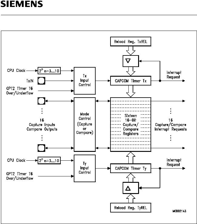
Capture/Compare (CAPCOM) Unit
The CAPCOM unit supports generation and control of timing sequences on up to 16 channels with a maximum resolution of 400 ns (@ 20 MHz CPU clock). The CAPCOM unit is typically used to handle high speed I/O tasks such as pulse and waveform generation, pulse width modulation (PMW), Digital to Analog (D/A) conversion, software timing, or time recording relative to external events.
Two 16-bit timers (T0/T1) with reload registers provide two independent time bases for the capture/ compare register array.
The input clock for the timers is programmable to several prescaled values of the CPU clock, or may be derived from an overflow/underflow of timer T6 in module GPT2. This provides a wide range of variation for the timer period and resolution and allows precise adjustments to the application specific requirements. In addition, an external count input for CAPCOM timer T0 allows event scheduling for the capture/compare registers relative to external events.
The capture/compare register array contains 16 dual purpose capture/compare registers, each of which may be individually allocated to either CAPCOM timer T0 or T1, and programmed for capture or compare function. Each register has one port pin associated with it which serves as an input pin for triggering the capture function, or as an output pin to indicate the occurence of a compare event.
When a capture/compare register has been selected for capture mode, the current contents of the allocated timer will be latched (captured) into the capture/compare register in response to an external event at the port pin which is associated with this register. In addition, a specific interrupt request for this capture/compare register is generated. Either a positive, a negative, or both a positive and a negative external signal transition at the pin can be selected as the triggering event. The contents of all registers which have been selected for one of the five compare modes are continuously compared with the contents of the allocated timers. When a match occurs between the timer value and the value in a capture/compare register, specific actions will be taken based on the selected compare mode.
Compare Modes |
Function |
|
|
Mode 0 |
Interrupt-only compare mode; |
|
several compare interrupts per timer period are possible |
|
|
Mode 1 |
Pin toggles on each compare match; |
|
several compare events per timer period are possible |
|
|
Mode 2 |
Interrupt-only compare mode; |
|
only one compare interrupt per timer period is generated |
|
|
Mode 3 |
Pin set ‘1’ on match; pin reset ‘0’ on compare time overflow; |
|
only one compare event per timer period is generated |
|
|
Double |
Two registers operate on one pin; pin toggles on each compare match; |
Register Mode |
several compare events per timer period are possible. |
|
|
Semiconductor Group |
15 |
SAB 80C166W/83C166W
x = 0 |
y = 1 |
Figure 5
CAPCOM-Unit Block Diagram
Semiconductor Group |
16 |
SAB 80C166W/83C166W
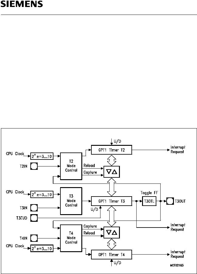
General Purpose Timer (GPT) Unit
The GPT unit represents a very flexible multifunctional timer/counter structure which may be used for many different time related tasks such as event timing and counting, pulse width and duty cycle measurements, pulse generation, or pulse multiplication.
The GPT unit incorporates five 16-bit timers which are organized in two separate modules, GPT1 and GPT2. Each timer in each module may operate independently in a number of different modes, or may be concatenated with another timer of the same module.
Each of the three timers T2, T3, T4 of module GPT1 can be configured individually for one of three basic modes of operation, which are Timer, Gated Timer, and Counter Mode. In Timer Mode, the input clock for a timer is derived from the CPU clock, divided by a programmable prescaler, while Counter Mode allows a timer to be clocked in reference to external events.
Pulse width or duty cycle measurement is supported in Gated Timer Mode, where the operation of a timer is controlled by the ‘gate’ level on an external input pin. For these purposes, each timer has one associated port pin (TxIN) which serves as gate or clock input. The maximum resolution of the timers in module GPT1 is 400 ns (@ 20 MHz CPU clock).
Figure 6
Block Diagram of GPT1
Semiconductor Group |
17 |
SAB 80C166W/83C166W
The count direction (up/down) for each timer is programmable by software. For timer T3 the count direction may additionally be altered dynamically by an external signal on a port pin (T3EUD) to facilitate e. g. position tracking.
Timer T3 has an output toggle latch (T3OTL) which changes its state on each timer overflow/ underflow. The state of this latch may be output on a port pin (T3OUT) e.g. for timeout monitoring of external hardware components, or may be used internally to clock timers T2 and T4 for measuring long time periods with high resolution.
In addition to their basic operating modes, timers T2 and T4 may be configured as reload or capture registers for timer T3. When used as capture or reload registers, timers T2 and T4 are stopped. The contents of timer T3 is captured into T2 or T4 in response to a signal at their associated input pins (TxIN). Timer T3 is reloaded with the contents of T2 or T4 triggered either by an external signal or by a selectable state transition of its toggle latch T3OTL. When both T2 and T4 are configured to alternately reload T3 on opposite state transitions of T3OTL with the low and high times of a PWM signal, this signal can be constantly generated without software intervention.
Figure 7
Block Diagram of GPT2
Semiconductor Group |
18 |

SAB 80C166W/83C166W
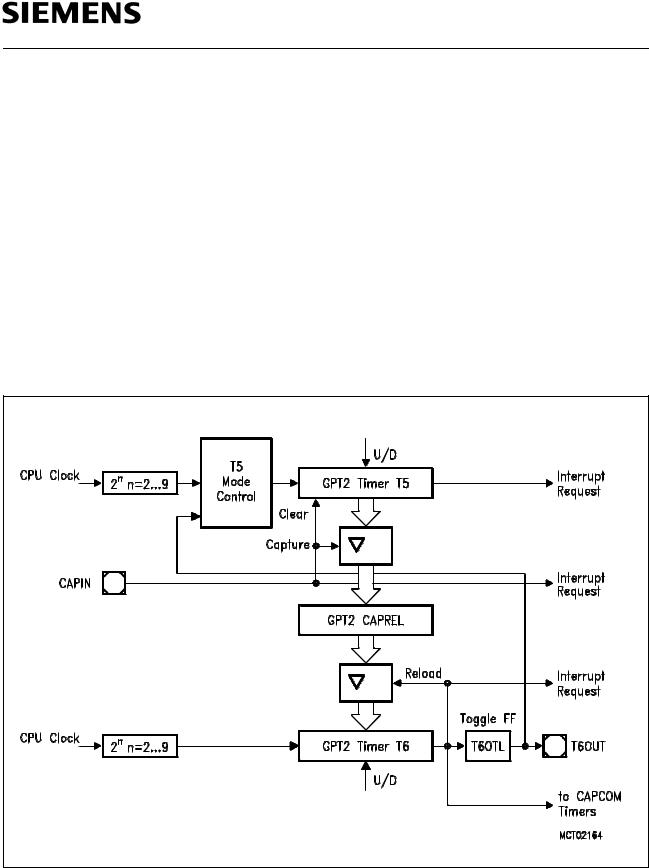
With its maximum resolution of 200 ns (@ 20 MHz), the GPT2 module provides precise event control and time measurement. It includes two timers (T5, T6) and a capture/reload register (CAPREL). Both timers can be clocked with an input clock which is derived from the CPU clock via a programmable prescaler. The count direction (up/down) for each timer is programmable by software. Concatenation of the timers is supported via the output toggle latch (T6OTL) of timer T6, which changes its state on each timer overflow/underflow.
The state of this latch may be used to clock timer T5, or it may be output on a port pin (T6OUT). The overflows/underflows of timer T6 can additionally be used to clock the CAPCOM timers T0 or T1, and to cause a reload from the CAPREL register. The CAPREL register may capture the contents of timer T5 based on an external signal transition on the corresponding port pin (CAPIN), and timer T5 may optionally be cleared after the capture procedure. This allows absolute time differences to be measured or pulse multiplication to be performed without software overhead.
A/D Converter
For analog signal measurement, a 10-bit A/D converter with 10 multiplexed input channels and a sample and hold circuit has been integrated on-chip. It uses the method of successive approximation. The sample time (for loading the capacitors) and the conversion time adds up to 9.7 us @ 20 MHz CPU clock.
Overrun error detection/protection is provided for the conversion result register (ADDAT): an interrupt request will be generated when the result of a previous conversion has not been read from the result register at the time the next conversion is complete.
For applications which require less than 10 analog input channels, the remaining channel inputs can be used as digital input port pins.
The A/D converter of the SAB 80C166W/83C166W supports four different conversion modes. In the standard Single Channel conversion mode, the analog level on a specified channel is sampled once and converted to a digital result. In the Single Channel Continuous mode, the analog level on a specified channel is repeatedly sampled and converted without software intervention. In the Auto Scan mode, the analog levels on a prespecified number of channels are sequentially sampled and converted. In the Auto Scan Continuous mode, the number of prespecified channels is repeatedly sampled and converted.
The Peripheral Event Controller (PEC) may be used to automatically store the conversion results into a table in memory for later evaluation, without requiring the overhead of entering and exiting interrupt routines for each data transfer.
Semiconductor Group |
19 |

SAB 80C166W/83C166W
Parallel Ports
The SAB 80C166W/83C166W provides up to 76 I/O lines which are organized into five input/output ports and one input port. All port lines are bit-addressable, and all input/output lines are individually (bit-wise) programmable as inputs or outputs via direction registers. The I/O ports are true bidirectional ports which are switched to high impedance state when configured as inputs. During the internal reset, all port pins are configured as inputs.
All port lines have programmable alternate input or output functions associated with them. Port 0 and Port 1 may be used as address and data lines when accessing external memory, while Port 4 outputs the additional segment address bits A17/A16 in systems where segmentation is enabled to access more than 64 KBytes of memory. Port 2 is associated with the capture inputs or compare outputs of the CAPCOM unit and/or with optional bus arbitration signals (BREQ, HLDA, HOLD). Port 3 includes alternate functions of timers, serial interfaces, optional bus control signals (WR, BHE, READY) and the system clock output (CLKOUT). Port 5 is used for the analog input channels to the A/D converter. All port lines that are not used for these alternate functions may be used as general purpose I/O lines.
Serial Channels
Serial communication with other microcontrollers, processors, terminals or external peripheral components is provided by two serial interfaces with identical functionality, Asynchronous/ Synchronous Serial Channels ASC0 and ASC1.
They are upward compatible with the serial ports of the Siemens SAB 8051x microcontroller family and support full-duplex asynchronous communication up to 625 Kbaud and half-duplex synchronous communication up to 2.5 Mbaud @ 20 MHz CPU clock.
Two dedicated baud rate generators allow to set up all standard baud rates without oscillator tuning. For transmission, reception, and erroneous reception 3 separate interrupt vectors are provided for each serial channel.
In asynchronous mode, 8- or 9-bit data frames are transmitted or received, preceded by a start bit and terminated by one or two stop bits. For multiprocessor communication, a mechanism to distinguish address from data bytes has been included (8-bit data + wake up bit mode).
In synchronous mode one data byte is transmitted or received synchronously to a shift clock which is generated by the SAB 80C166W/83C166W.
A loop back option is available for testing purposes.
A number of optional hardware error detection capabilities has been included to increase the reliability of data transfers. A parity bit can automatically be generated on transmission or be checked on reception. Framing error detection allows to recognize data frames with missing stop bits. An overrun error will be generated, if the last character received has not been read out of the receive buffer register at the time the reception of a new character is complete.
Semiconductor Group |
20 |
SAB 80C166W/83C166W
Watchdog Timer
The Watchdog Timer represents one of the fail-safe mechanisms which have been implemented to prevent the controller from malfunctioning for longer periods of time.
The Watchdog Timer is always enabled after a reset of the chip, and can only be disabled in the time interval until the EINIT (end of initialization) instruction has been executed. Thus, the chip’s start-up procedure is always monitored. The software has to be designed to service the Watchdog Timer before it overflows. If, due to hardware or software related failures, the software fails to do so, the Watchdog Timer overflows and generates an internal hardware reset and pulls the RSTOUT pin low in order to allow external hardware components to be reset.
The Watchdog Timer is a 16-bit timer, clocked with the CPU clock divided either by 2 or by 128. The high byte of the Watchdog Timer register can be set to a prespecified reload value (stored in WDTREL) in order to allow further variation of the monitored time interval. Each time it is serviced by the application software, the high byte of the Watchdog Timer is reloaded. Thus, time intervals between 25 μs and 420 ms can be monitored (@ 20 MHz CPU clock). The default Watchdog Timer interval after reset is 6.55 ms (@ 20 MHz CPU clock).
Bootstrap Loader
The SAB 80C166W/83C166W provides a built-in bootstrap loader (BSL), which allows to start program execution out of the SAB 80C166W/83C166W’s internal RAM. This start program is loaded via the serial interface ASC0 and does not require external memory or an internal ROM.
The SAB 80C166W/83C166W enters BSL mode, when ALE is sampled high at the end of a hardware reset and if NMI becomes active directly after the end of the internal reset sequence. BSL mode is entered independent of the bus mode selected via EBC0, EBC1 and BUSACT.
After entering BSL mode the SAB 80C166W/83C166W scans the RXD0 line to receive a zero byte, ie. one start bit, eight ‘0’ data bits and one stop bit. From the duration of this zero byte it calculates the corresponding baudrate factor with respect to the current CPU clock and initializes ASC0 accordingly. Using this baudrate, an acknowledge byte is returned to the host that provides the loaded data. The SAB 80C166W/83C166W returns the value <55H>.
The next 32 bytes received via ASC0 are stored sequentially into locations 0FA40H through 0FA5FH of the internal RAM. To execute the loaded code the BSL then jumps to location 0FA40H. The loaded program may load additional code / data, change modes, etc.
The SAB 80C166W/83C166W exits BSL mode upon a software reset (ignores the ALE level) or a hardware reset (remove conditions for entering BSL mode before).
Instruction Set Summary
The summary on the following pages lists the instructions of the SAB 80C166W/83C166W ordered into logical groups.
Semiconductor Group |
21 |
 Loading...