


Siemens SAB-C515A-4R24M, SAB-C515A-4RM, SAB-C515A-L24M, SAB-C515A-LM, SAF-C515A-4R24M Datasheet
...Microcomputer Components
8-Bit CMOS Microcontroller
C515A
Data Sheet 10.97
C515A Data Sheet |
|
|
Revision History: |
Current Version: 10.97 |
|
|
|
|
Previous Version: |
none |
|
|
|
|
Page |
Page |
Subjects (major changes since last revision) |
(in previous |
(in current |
|
Version) |
Version) |
|
|
|
|
|
|
|
|
|
|
Edition 10.97
Published by Siemens AG, Bereich Halbleiter, MarketingKommunikation, Balanstraße 73, 81541 München
© Siemens AG 1997.
All Rights Reserved.
Attention please!
As far as patents or other rights of third parties are concerned, liability is only assumed for components, not for applications, processes and circuits implemented within components or assemblies.
The information describes the type of component and shall not be considered as assured characteristics. Terms of delivery and rights to change design reserved.
For questions on technology, delivery and prices please contact the Semiconductor Group Offices in Germany or the Siemens Companies and Representatives worldwide (see address list).
Due to technical requirements components may contain dangerous substances. For information on the types in question please contact your nearest Siemens Office, Semiconductor Group.
Siemens AG is an approved CECC manufacturer.
Packing
Please use the recycling operators known to you. We can also help you – get in touch with your nearest sales office. By agreement we will take packing material back, if it is sorted. You must bear the costs of transport.
For packing material that is returned to us unsorted or which we are not obliged to accept, we shall have to invoice you for any costs incurred.
Components used in life-support devices or systems must be expressly authorized for such purpose!
Critical components1 of the Semiconductor Group of Siemens AG, may only be used in life-support devices or systems2 with the express written approval of the Semiconductor Group of Siemens AG.
1A critical component is a component used in a life-support device or system whose failure can reasonably be expected to cause the failure of that life-support device or system, or to affect its safety or effectiveness of that device or system.
2Life support devices or systems are intended (a) to be implanted in the human body, or (b) to support and/or maintain and sustain human life. If they fail, it is reasonable to assume that the health of the user may be endangered.
8-Bit CMOS Microcontroller |
C515A |
Advance Information
•Full upward compatibility with SAB 80C515A/83C515A-5
•Up to 24 MHz external operating frequency
–500 ns instruction cycle at 24 MHz operation
•32K byte on-chip ROM (with optional ROM protection)
–alternatively up to 64K byte external program memory
•Up to 64K byte external data memory
•256 byte on-chip RAM
•1K byte on-chip RAM (XRAM)
•Six 8-bit parallel I/O ports
•One input port for analog/digital input
•Full duplex serial interface (USART)
–4 operating modes, fixed or variable baud rates
•Three 16-bit timer/counters
–Timer 0 / 1 (C501 compatible)
–Timer 2 for 16-bit reload, compare, or capture functions
(further features are on next page)
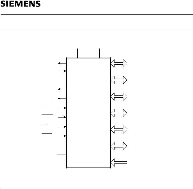
Support Module
On-Chip Emulation
Oscillator |
|
Watchdog |
XRAM |
|
|
RAM |
Port 0 |
I / O |
|||||
Watchdog |
|
Timer |
|
1 K x 8 |
|
|
256 x 8 |
||||||
|
|
|
|
|
|
||||||||
|
|
|
|
|
|
|
|
|
|
|
|
|
I / O |
|
|
|
|
|
|
T 0 |
|
|
|
|
|
Port 1 |
|
|
10-Bit |
|
|
T 2 |
|
|
CPU |
|
USART |
|
|
||
Power |
A / D Converter |
|
|
|
|
|
I / O |
||||||
|
|
|
|
|
|
|
|
|
|||||
Saving |
|
|
|
|
|
T 1 |
|
|
|
|
|
Port 2 |
|
Modes |
|
|
|
|
|
|
|
|
|
|
|
|
|
|
Port 6 |
Port 5 |
Port 4 |
|
|
ROM |
|
|
Port 3 |
I / O |
|||
|
|
|
32 k x 8 |
||||||||||
|
|
|
|
|
|
|
|
|
|
||||
|
|
|
|
|
|
|
|
|
|
|
|
|
|
Analog / I / O |
I / O |
Digital |
|
Input |
MCA03239 |
Figure 1
C515A Functional Units
Semiconductor Group |
3 |
1997-10-01 |

C515A
Features (cont’d):
•10-bit A/D converter
–8 multiplexed analog inputs
–Built-in self calibration
•16-bit watchdog timer
•Power saving modes
–Slow down mode
–Idle mode (can be combined with slow down mode)
–Software power down mode with wake-up capability through INT0 pin
–Hardware power down mode
•12 interrupt sources (7 external, 5 internal) selectable at 4 priority levels
•ALE switch-off capability
•On-chip emulation support logic (Enhanced Hooks Technology TM)
•P-MQFP-80-1 package
•Temperature Ranges: SAB-C515A TA = 0 to 70 °C
SAF-C515A SAH-C515A SAK-C515
TA = – 40 to 85 °C TA = – 40 to 85 °C
TA = – 40 to 110 °C (max. operating frequency: 18 MHz)
The C515A is an upward compatible version of the SAB 80C515A/83C515A-5 8-bit microcontroller which additionally provides an improved 10-bit A/D converter, ALE switch-off capability, on-chip emulation support, ROM protection, and enhanced power saving mode capabilities. With a maximum external clock rate of 24 MHz it achieves a 500 ns instruction cycle time (1 s at 12 MHz). The C515A is mounted in a P-MQFP-80 package.
Ordering Information
Type |
Ordering Code |
Package |
Description |
|
|
|
(8-Bit CMOS microcontroller) |
|
|
|
|
SAB-C515A-4RM |
Q67121-DXXXX |
P-MQFP-80-1 |
with mask programmable ROM (18 MHz) |
|
|
|
|
SAF-C515A-4RM |
Q67121-DXXXX |
P-MQFP-80-1 |
with mask programmable ROM (18 MHz) |
|
|
|
ext. temp. – 40 °C to 85 °C |
SAB-C515A-4R24M |
Q67121-DXXXX |
P-MQFP-80-1 |
with mask programmable ROM (24 MHz) |
|
|
|
|
SAF-C515A-4R24M |
Q67121-DXXXX |
P-MQFP-80-1 |
with mask programmable ROM (24 MHz) |
|
|
|
ext. temp. – 40 °C to 85 °C |
SAB-C515A-LM |
Q67121-C1068 |
P-MQFP-80-1 |
for external memory (18 MHz) |
|
|
|
|
SAF-C515A-LM |
Q67121-C1069 |
P-MQFP-80-1 |
for external memory (18 MHz) |
|
|
|
ext. temp. – 40 °C to 85 °C |
SAB-C515A-L24M |
Q67121-C1070 |
P-MQFP-80-1 |
for external memory (24 MHz) |
|
|
|
|
SAF-C515A-L24M |
Q67127-C2020 |
P-MQFP-80-1 |
for external memory (24 MHz) |
|
|
|
ext. temp. – 40 °C to 85 °C |
Note: Versions for extended temperature ranges – 40 °C to 110 °C and – 40 °C to 125 °C (SAH-C515A and SAK-C515A) are available on request. The ordering number of ROM types (DXXXX extensions) is defined after program release (verification) of the customer.
Semiconductor Group |
4 |
1997-10-01 |
C515A
V CC |
|
V SS |
|
XTAL1 |
|
Port 0 |
|
|
8-Bit Digit. I / O |
||
|
|
||
XTAL2 |
|
|
|
|
|
Port 1 |
|
|
|
8-Bit Digit. I / O |
|
ALE |
|
|
|
PSEN |
|
Port 2 |
|
|
8-Bit Digit. I / O |
||
EA |
C515A |
Port 3 |
|
|
|||
RESET |
8-Bit Digit. I / O |
||
|
|||
|
|
||
PE / SWD |
|
Port 4 |
|
HWPD |
|
8-Bit Digit. I / O |
|
|
|
||
|
|
Port 5 |
|
|
|
8-Bit Digit. I / O |
|
V AREF |
|
Port 6 |
|
V AGND |
|
8-Bit Analog / |
|
|
|
Digital Input |
|
|
|
MCL03240 |
Figure 2
Logic Symbol
Additional Literature
For further information about the C515A the following literature is available:
Title |
|
Ordering Number |
|
|
|
C515A 8-Bit CMOS Microcontroller User’s Manual |
B158-H7051-X-X-7600 |
|
|
|
|
C500 |
Microcontroller Family |
B158-H6987-X-X-7600 |
Architecture and Instruction Set User’s Manual |
|
|
|
|
|
C500 |
Microcontroller Family - Pocket Guide |
B158-H6986-X-X-7600 |
|
|
|
Semiconductor Group |
5 |
1997-10-01 |
C515A
|
|
|
|
|
|
|
|
P5.7 |
P0.7 / AD7 |
P0.6 / AD6 |
P0.5 / AD5 |
P0.4 / AD4 |
P0.3 / AD3 |
P0.2 / AD2 |
P0.1 / AD1 |
P0.0 / AD0 |
N.C. N.C. |
|
EA ALE |
|
PSEN N.C. P2.7 / A15 P2.6 / A14 P2.5 / A13 P2.4 / A12 P2.3 / A11 |
|
|
|
|
|
|
|
|
|
|
|
|
|
|
|
|
|
|
|
|
|
|
|
|
|
|
||||||||||||
|
|
|
|
|
|
|
|
|
|
|
|
|
|
|
|
|
|||||||||||||
|
|
|
|
P5.6 |
60 59 58 57 56 55 54 53 52 51 50 49 48 47 46 45 44 43 42 41 |
|
|
P2.2 |
/ A10 |
||||||||||||||||||||
|
|
|
|
|
|
61 |
|
|
|
|
|
|
|
|
|
|
|
|
|
40 |
|
|
|||||||
|
|
|
|
|
|
|
|
|
|
|
|
|
|
|
|
|
|||||||||||||
|
|
|
|
|
|
|
|
|
|
|
|
|
|
|
|
|
|||||||||||||
|
|
|
|
P5.5 |
|
62 |
|
|
|
|
|
|
|
|
|
|
|
|
|
39 |
|
|
P2.1 |
/ A9 |
|||||
|
|
|
|
|
|
|
|
|
|
|
|
|
|
|
|
|
|||||||||||||
|
|
|
|
|
|
|
|
|
|
|
|
|
|
|
|
||||||||||||||
|
|
|
|
P5.4 |
|
63 |
|
|
|
|
|
|
|
|
|
|
|
|
|
38 |
|
|
P2.0 |
/ A8 |
|||||
|
|
|
|
|
|
|
|
|
|
|
|
|
|
|
|
|
|||||||||||||
|
|
|
|
|
|
|
|
|
|
|
|
|
|
|
|
||||||||||||||
|
|
|
|
P5.3 |
|
64 |
|
|
|
|
|
|
|
|
|
|
|
|
|
37 |
|
|
XTAL1 |
||||||
|
|
|
|
|
|
|
|
|
|
|
|
|
|
|
|
|
|||||||||||||
|
|
|
|
|
|
|
|
|
|
|
|
|
|
|
|
||||||||||||||
|
|
|
|
P5.2 |
|
65 |
|
|
|
|
|
|
|
|
|
|
|
|
|
36 |
|
|
XTAL2 |
||||||
|
|
|
|
|
|
|
|
|
|
|
|
|
|
|
|
|
|||||||||||||
|
|
|
|
|
|
|
|
|
|
|
|
|
|
|
|
||||||||||||||
|
|
|
|
P5.1 |
|
66 |
|
|
|
|
|
|
|
|
|
|
|
|
|
35 |
|
|
VSS |
|
|
|
|
||
|
|
|
|
|
|
|
|
|
|
|
|
|
|
|
|
|
|
|
|
|
|||||||||
|
|
|
|
|
|
|
|
|
|
|
|
|
|
|
|
|
|
|
|
||||||||||
|
|
|
|
P5.0 |
|
67 |
|
|
|
|
|
|
|
|
|
|
|
|
|
34 |
|
|
VSS |
|
|
|
|
||
|
|
|
|
|
|
|
|
|
|
|
|
|
|
|
|
|
|
|
|
|
|||||||||
|
|
|
|
|
|
|
|
|
|
|
|
|
|
|
|
|
|
|
|
||||||||||
|
|
|
|
N.C. |
|
|
68 |
|
|
|
|
|
|
|
|
|
|
|
|
|
33 |
|
|
VCC |
|
|
|
|
|
|
|
|
|
|
|
|
|
|
|
|
|
|
|
|
|
|
|
|
|
|
|||||||||
|
|
|
|
|
|
|
|
|
|
|
|
|
|
|
|
|
|
|
|
||||||||||
|
|
HWPD |
|
69 |
|
|
|
|
|
|
|
|
|
|
|
|
|
32 |
|
|
VCC |
|
|
|
|
||||
|
|
|
|
|
|
|
|
|
|
|
|
|
|
|
|
|
|
|
|
|
|||||||||
|
|
|
|
|
|
|
|
|
|
|
|
|
|
|
|
|
|
|
|
||||||||||
|
|
|
|
N.C. |
|
|
70 |
|
|
|
|
|
|
|
|
C515A |
31 |
|
|
P1.0 |
/ |
INT3 |
/ CC0 |
||||||
|
|
|
|
|
|
|
|
|
|
|
|
||||||||||||||||||
|
|
|
|
|
|
|
|
|
|
|
|||||||||||||||||||
|
|
|
|
N.C. |
|
|
|
71 |
|
|
|
|
|
|
|
|
30 |
|
|
P1.1 |
/ INT4 / CC1 |
||||||||
|
|
|
|
|
|
|
|
|
|
|
|
|
|
|
|
|
|
|
|
|
|||||||||
P4.0 / ADST |
|
|
72 |
|
|
|
|
|
|
|
|
|
|
|
|
|
29 |
|
|
P1.2 |
/ INT5 / CC2 |
||||||||
|
|
|
|
|
|
|
|
|
|
|
|
|
|
|
|
|
|||||||||||||
|
|
|
|
|
|
|
|
|
|
|
|
|
|
|
|
||||||||||||||
|
|
|
|
P4.1 |
|
73 |
|
|
|
|
|
|
|
|
|
|
|
|
|
28 |
|
|
P1.3 |
/ INT6 / CC3 |
|||||
|
|
|
|
|
|
|
|
|
|
|
|
|
|
|
|
|
|||||||||||||
|
|
|
|
|
|
|
|
|
|
|
|
|
|
|
|
||||||||||||||
|
|
|
|
P4.2 |
|
74 |
|
|
|
|
|
|
|
|
|
|
|
|
|
27 |
|
|
P1.4 |
/ INT2 |
|||||
|
|
|
|
|
|
|
|
|
|
|
|
|
|
|
|
||||||||||||||
|
|
|
|
|
|
|
|
|
|
|
|
|
|
|
|
||||||||||||||
PE / SWD |
|
|
75 |
|
|
|
|
|
|
|
|
|
|
|
|
|
26 |
|
|
P1.5 |
/ T2EX |
||||||||
|
|
|
|
|
|
|
|
|
|
|
|
|
|
|
|
||||||||||||||
|
|
|
|
|
|
|
|
|
|
|
|
|
|
|
|
||||||||||||||
|
|
|
|
P4.3 |
|
76 |
|
|
|
|
|
|
|
|
|
|
|
|
|
25 |
|
|
P1.6 |
/ CLKOUT |
|||||
|
|
|
|
|
|
|
|
|
|
|
|
|
|
|
|
||||||||||||||
|
|
|
|
|
|
|
|
|
|
|
|
|
|
|
|
||||||||||||||
|
|
|
|
P4.4 |
|
77 |
|
|
|
|
|
|
|
|
|
|
|
|
|
24 |
|
|
P1.7 |
/ T2 |
|||||
|
|
|
|
|
|
|
|
|
|
|
|
|
|
|
|
|
|||||||||||||
|
|
|
|
|
|
|
|
|
|
|
|
|
|
|
|
||||||||||||||
|
|
|
|
P4.5 |
|
78 |
|
|
|
|
|
|
|
|
|
|
|
|
|
23 |
|
|
N.C. |
|
|
|
|
||
|
|
|
|
|
|
|
|
|
|
|
|
|
|
|
|
|
|
|
|
|
|||||||||
|
|
|
|
|
|
|
|
|
|
|
|
|
|
|
|
|
|
|
|
||||||||||
|
|
|
|
P4.6 |
|
|
79 |
|
|
|
|
|
|
|
|
|
|
|
|
|
22 |
|
|
P3.7 |
/ |
RD |
|
|
|
|
|
|
|
|
|
|
|
|
|
|
|
|
|
|
|
|
|||||||||||||
|
|
|
|
|
|
|
|
|
|
|
|
|
|
|
|
||||||||||||||
|
|
|
|
P4.7 |
|
80 |
2 |
3 |
4 |
5 |
6 |
7 |
8 |
9 |
|
|
|
|
|
21 |
|
|
P3.6 |
/ WR |
|||||
|
|
|
|
|
|
|
|
|
|||||||||||||||||||||
|
|
|
|
|
|
1 |
10 11 12 13 14 15 16 17 18 19 20 |
|
|
|
|
|
|
|
|||||||||||||||
RESET N.C. V V |
/P6.7AIN7 |
/P6.6AIN6 /P6.5AIN5 /P6.4AIN4 /P6.3AIN3 /P6.2AIN2 |
/P6.1AIN1 /P6.0AIN0 N.C. N.C. P3.0/ RxD P3.1/ TxD /P3.2INT0 P3.3/ INT1 P3.4/ T0 P3.5/ T1 |
||||
AREF AGND |
|
|
|
|
|
|
|
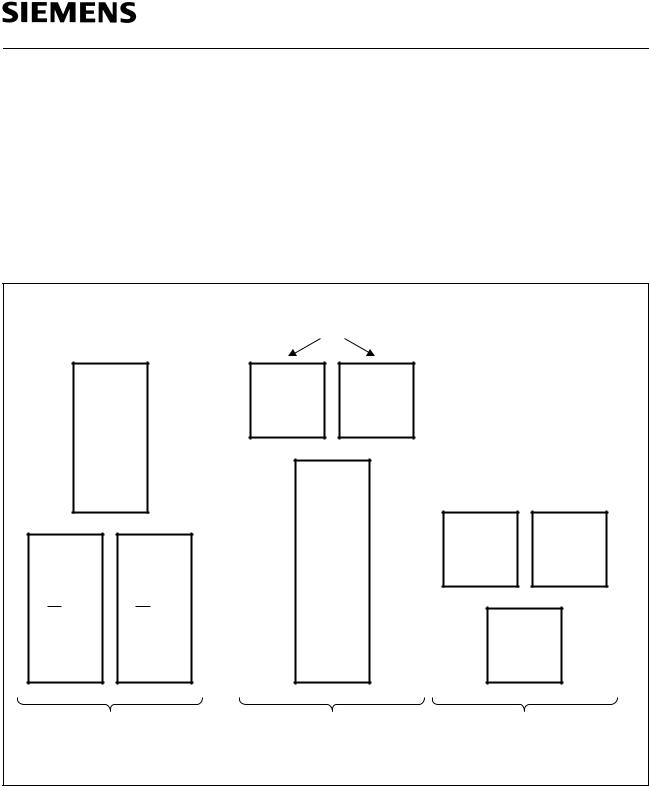
MCP03241
Figure 3
Pin Configuration P-MQFP-80 Package (top view)
Semiconductor Group |
6 |
1997-10-01 |

C515A
Table 1
Pin Definitions and Functions
Symbol |
Pin Number |
I/O*) |
|
Function |
|
|
||||||
|
|
|
(P-MQFP-80) |
|
|
|
|
|
|
|
|
|
|
|
|
|
|
|
|
||||||
P4.0-P4.7 |
72-74, |
I/O |
|
Port 4 |
|
|
||||||
|
|
|
76-80 |
|
|
is an 8-bit quasi-bidirectional I/O port with internal pull- |
||||||
|
|
|
|
|
|
up resistors. Port 4 pins that have 1’s written to them are |
||||||
|
|
|
|
|
|
pulled high by the internal pull-up resistors, and in that |
||||||
|
|
|
|
|
|
state can be used as inputs. As inputs, port 4 pins being |
||||||
|
|
|
|
|
|
externally pulled low will source current (I IL, in the DC |
||||||
|
|
|
|
|
|
characteristics) because of the internal pull-up resistors. |
||||||
|
|
|
|
|
|
P4 also contains the external A/D converter control pin. |
||||||
|
|
|
|
|
|
The output latch corresponding to a secondary function |
||||||
|
|
|
|
|
|
must be programmed to a one (1) for that function to |
||||||
|
|
|
|
|
|
operate. The secondary function is assigned to port 6 as |
||||||
|
|
|
|
|
|
follows: |
|
|
||||
|
|
|
72 |
|
|
P4.0 / |
|
|
|
external A/D converter start pin |
||
|
|
|
|
ADST |
||||||||
|
|
|
|
|
|
|
|
|
|
|||
|
|
|
75 |
I |
|
|
|
|
|
|
|
/ Start Watchdog Timer |
PE/SWD |
Power Saving Mode Enable |
|||||||||||
|
|
|
|
|
|
A low level on this pin allows the software to enter the |
||||||
|
|
|
|
|
|
power down, idle, and slow down mode. In case the low |
||||||
|
|
|
|
|
|
level is also seen during reset, the watchdog timer |
||||||
|
|
|
|
|
|
function is off on default. |
||||||
|
|
|
|
|
|
Use of the software controlled power saving modes is |
||||||
|
|
|
|
|
|
blocked when this pin is held on high level. A high level |
||||||
|
|
|
|
|
|
during reset performs an automatic start of the |
||||||
|
|
|
|
|
|
watchdog timer immediately after reset. |
||||||
|
|
|
|
|
|
When left unconnected this pin is pulled high by a weak |
||||||
|
|
|
|
|
|
internal pull-up resistor. |
||||||
|
|
|
|
|
Note: If |
|
|
|||||
|
|
|
|
|
PE/SWD is low and VAREF is low the oscillator |
|||||||
|
|
|
|
|
watchdog is disabled (testmode)! |
|||||||
|
|
|
|
|
|
|
|
|
||||
|
|
|
1 |
I |
|
|
|
|
|
|||
RESET |
|
RESET |
|
|
||||||||
|
|
|
|
|
|
A low level on this pin for the duration of two machine |
||||||
|
|
|
|
|
|
cycles while the oscillator is running resets the C515A. |
||||||
|
|
|
|
|
|
A small internal pullup resistor permits power-on reset |
||||||
|
|
|
|
|
|
using only a capacitor connected to VSS . |
||||||
VAREF |
3 |
– |
|
Reference Voltage for the A/D converter |
||||||||
|
|
|
|
|
||||||||
VAGND |
4 |
– |
|
Reference Ground for the A/D converter |
||||||||
|
|
|
|
|
|
|
||||||
P6.0-P6.7 |
12-5 |
I |
|
Port 6 |
|
|
||||||
|
|
|
|
|
|
is an 8-bit unidirectional input port to the A/D converter. |
||||||
|
|
|
|
|
|
Port pins can be used for digital input, if voltage levels |
||||||
|
|
|
|
|
|
simultaneously meet the specifications for high/low input |
||||||
|
|
|
|
|
|
voltages and for the eight multiplexed analog inputs. |
||||||
|
|
|
|
|
|
|
|
|
|
|
||
*) I = Input |
|
|
|
|
|
|
|
|
|
|
||
|
O = Output |
|
|
|
|
|
|
|
|
|
|
|
Semiconductor Group |
|
7 |
|
1997-10-01 |
||||||||

C515A
Table 1
Pin Definitions and Functions (cont’d)
Symbol |
Pin Number |
I/O*) |
Function |
|
|
|
|
||||
|
(P-MQFP-80) |
|
|
|
|
|
|
|
|
|
|
|
|
|
|
|
|
|
|
|
|
|
|
P3.0-P3.7 |
15-22 |
I/O |
Port 3 |
|
|
|
|
|
|
|
|
|
|
|
is an 8-bit quasi-bidirectional I/O port with internal pullup |
||||||||
|
|
|
resistors. Port 3 pins that have 1's written to them are |
||||||||
|
|
|
pulled high by the internal pullup resistors, and in that |
||||||||
|
|
|
state can be used as inputs. As inputs, port 3 pins being |
||||||||
|
|
|
externally pulled low will source current (I IL, in the DC |
||||||||
|
|
|
characteristics) because of the internal pullup resistors. |
||||||||
|
|
|
Port 3 also contains the interrupt, timer, serial port and |
||||||||
|
|
|
external memory strobe pins that are used by various |
||||||||
|
|
|
options. The output latch corresponding to a secondary |
||||||||
|
|
|
function must be programmed to a one (1) for that |
||||||||
|
|
|
function to operate. The secondary functions are |
||||||||
|
|
|
assigned to the pins of port 3, as follows: |
||||||||
|
15 |
|
P3.0 |
/ RxD |
|
Receiver data input (asynch.) |
|||||
|
|
|
|
|
|
|
|
|
or data input/output (synch.) |
||
|
|
|
|
|
|
|
|
|
of serial interface |
||
|
16 |
|
P3.1 |
/ TxD |
|
Transmitter data output |
|||||
|
|
|
|
|
|
|
|
|
(asynch.) or clock output |
||
|
|
|
|
|
|
|
|
|
(synch.) of serial interface |
||
|
17 |
|
P3.2 |
/ |
|
|
|
|
External interrupt 0 input / |
||
|
|
INT0 |
|||||||||
|
|
|
|
|
|
|
|
|
timer 0 gate control input |
||
|
18 |
|
P3.3 |
/ |
|
|
|
|
External interrupt 1 input / |
||
|
|
INT1 |
|||||||||
|
|
|
|
|
|
|
|
|
timer 1 gate control input |
||
|
19 |
|
P3.4 |
/ T0 |
|
Timer 0 counter input |
|||||
|
20 |
|
P3.5 |
/ T1 |
|
Timer 1 counter input |
|||||
|
21 |
|
P3.6 |
/ |
|
|
|
|
|
|
control output; latches |
|
|
WR |
WR |
||||||||
|
|
|
|
|
|
|
|
|
the data byte from port 0 into |
||
|
|
|
|
|
|
|
|
|
the external data memory |
||
|
22 |
|
P3.7 |
/ |
|
|
|
|
control output; enables |
||
|
|
RD |
|
RD |
|||||||
|
|
|
|
|
|
|
|
|
the external data memory |
||
|
|
|
|
|
|
|
|
|
|
|
|
*) I = Input |
|
|
|
|
|
|
|
|
|
|
|
O = Output |
|
|
|
|
|
|
|
|
|
|
|
Semiconductor Group |
8 |
1997-10-01 |

C515A
Table 1
Pin Definitions and Functions (cont’d)
Symbol |
Pin Number |
I/O*) |
Function |
|
||
|
(P-MQFP-80) |
|
|
|
|
|
|
|
|
|
|
||
P1.0 - P1.7 |
31-24 |
I/O |
Port 1 |
|
||
|
|
|
is an 8-bit quasi-bidirectional I/O port with internal pullup |
|||
|
|
|
resistors. Port 1 pins that have 1's written to them are |
|||
|
|
|
pulled high by the internal pullup resistors, and in that |
|||
|
|
|
state can be used as inputs. As inputs, port 1 pins being |
|||
|
|
|
externally pulled low will source current (I IL, in the DC |
|||
|
|
|
characteristics) because of the internal pullup resistors. |
|||
|
|
|
The port is used for the low-order address byte during |
|||
|
|
|
program verification. Port 1 also contains the interrupt, |
|||
|
|
|
timer, clock, capture and compare pins that are used by |
|||
|
|
|
various options. The output latch corresponding to a |
|||
|
|
|
secondary function must be programmed to a one (1) for |
|||
|
|
|
that function to operate (except when used for the |
|||
|
|
|
compare functions). The secondary functions are |
|||
|
|
|
assigned to the port 1 pins as follows: |
|||
|
31 |
|
P1.0 / |
|
/ CC0 |
Interrupt 3 input / |
|
|
INT3 |
||||
|
|
|
|
|
|
compare 0 output / |
|
|
|
|
|
|
capture 0 input |
|
30 |
|
P1.1 / INT4 / CC1 |
Interrupt 4 input / |
||
|
|
|
|
|
|
compare 1 output / |
|
|
|
|
|
|
capture 1 input |
|
29 |
|
P1.2 / INT5 / CC2 |
Interrupt 5 input / |
||
|
|
|
|
|
|
compare 2 output / |
|
|
|
|
|
|
capture 2 input |
|
28 |
|
P1.3 / INT6 / CC3 |
Interrupt 6 input / |
||
|
|
|
|
|
|
compare 3 output / |
|
|
|
|
|
|
capture 3 input |
|
27 |
|
P1.4 / |
|
|
Interrupt 2 input |
|
|
INT2 |
||||
|
26 |
|
P1.5 / T2EX |
Timer 2 external reload / |
||
|
|
|
|
|
|
trigger input |
|
25 |
|
P1.6 / CLKOUT |
System clock output |
||
|
24 |
|
P1.7 / T2 |
Counter 2 input |
||
|
|
|
|
|
||
VCC |
32, 33 |
– |
Supply Voltage |
|
||
|
|
|
during normal, idle, and power down mode. |
|||
|
|
|
|
|
||
VSS |
34, 35 |
– |
Ground (0V) |
|
||
|
|
|
during normal, idle, and power down operation. |
|||
|
|
|
|
|
|
|
*) I = Input |
|
|
|
|
|
|
O = Output |
|
|
|
|
|
|
Semiconductor Group |
9 |
1997-10-01 |

C515A
Table 1
Pin Definitions and Functions (cont’d)
Symbol |
Pin Number |
I/O*) |
Function |
|||
|
|
(P-MQFP-80) |
|
|
|
|
|
|
|
|
|||
XTAL2 |
36 |
– |
XTAL2 |
|||
|
|
|
|
Input to the inverting oscillator amplifier and input to the |
||
|
|
|
|
internal clock generator circuits. To drive the device |
||
|
|
|
|
from an external clock source, XTAL2 should be driven, |
||
|
|
|
|
while XTAL1 is left unconnected. Minimum and |
||
|
|
|
|
maximum high and low times as well as rise/fall times |
||
|
|
|
|
specified in the AC characteristics must be observed. |
||
|
|
|
|
|||
XTAL1 |
37 |
– |
XTAL1 |
|||
|
|
|
|
Output of the inverting oscillator amplifier. |
||
|
|
|
|
|||
P2.0-P2.7 |
38-45 |
I/O |
Port 2 |
|||
|
|
|
|
is an 8-bit quasi-bidirectional I/O port with internal pullup |
||
|
|
|
|
resistors. Port 2 pins that have 1's written to them are |
||
|
|
|
|
pulled high by the internal pullup resistors, and in that |
||
|
|
|
|
state can be used as inputs. As inputs, port 2 pins being |
||
|
|
|
|
externally pulled low will source current (I IL, in the DC |
||
|
|
|
|
characteristics) because of the internal pullup resistors. |
||
|
|
|
|
Port 2 emits the high-order address byte during fetches |
||
|
|
|
|
from external program memory and during accesses to |
||
|
|
|
|
external data memory that use 16-bit addresses |
||
|
|
|
|
(MOVX @DPTR). In this application it uses strong |
||
|
|
|
|
internal pullup resistors when issuing 1's. During |
||
|
|
|
|
accesses to external data memory that use 8-bit |
||
|
|
|
|
addresses (MOVX @Ri), port 2 issues the contents of |
||
|
|
|
|
the P2 special function register. |
||
|
|
|
|
|
|
|
|
|
47 |
O |
The |
|
|
PSEN |
Program Store Enable |
|||||
|
|
|
|
output is a control signal that enables the external |
||
|
|
|
|
program memory to the bus during external fetch |
||
|
|
|
|
operations. It is activated every six oscillator periods, |
||
|
|
|
|
except during external data memory accesses. The |
||
|
|
|
|
signal remains high during internal program execution. |
||
|
|
|
|
|||
ALE |
48 |
O |
The Address Latch Enable |
|||
|
|
|
|
output is used for latching the address into external |
||
|
|
|
|
memory during normal operation. It is activated every |
||
|
|
|
|
six oscillator periods, except during an external data |
||
|
|
|
|
memory access. ALE can be switched off when the |
||
|
|
|
|
program is executed internally. |
||
|
|
|
|
|
|
|
*) I = Input |
|
|
|
|
|
|
O = Output |
|
|
|
|
|
|
Semiconductor Group |
10 |
1997-10-01 |
C515A
Table 1
Pin Definitions and Functions (cont’d)
Symbol |
Pin Number |
I/O*) |
|
Function |
||||
|
|
|
(P-MQFP-80) |
|
|
|
|
|
|
|
|
|
|
|
|
|
|
|
|
|
49 |
I |
|
|
|
|
EA |
External Access Enable |
|||||||
|
|
|
|
|
|
When held high, the C515A executes instructions from |
||
|
|
|
|
|
|
the internal ROM (C515A-4R) as long as the PC is less |
||
|
|
|
|
|
|
than 8000H. When held low, the C515A fetches all |
||
|
|
|
|
|
|
instructions from external program memory. For the |
||
|
|
|
|
|
|
C515A-L this pin must be tied low. |
||
|
|
|
|
|
||||
P0.0-P0.7 |
52-59 |
I/O |
|
Port 0 |
||||
|
|
|
|
|
|
is an 8-bit open-drain bidirectional I/O port. Port 0 pins |
||
|
|
|
|
|
|
that have 1's written to them float, and in that state can |
||
|
|
|
|
|
|
be used as high-impedance inputs. |
||
|
|
|
|
|
|
Port 0 is also the multiplexed low-order address and |
||
|
|
|
|
|
|
data bus during accesses to external program and data |
||
|
|
|
|
|
|
memory. In this application it uses strong internal pullup |
||
|
|
|
|
|
|
resistors when issuing 1's. Port 0 also outputs the code |
||
|
|
|
|
|
|
bytes during program verification in the C515A-4R. |
||
|
|
|
|
|
|
External pullup resistors are required during program |
||
|
|
|
|
|
|
verification. |
||
|
|
|
|
|
||||
P5.0-P5.7 |
67-60 |
I/O |
|
Port 5 |
||||
|
|
|
|
|
|
is an 8-bit quasi-bidirectional I/O port with internal pullup |
||
|
|
|
|
|
|
resistors. Port 5 pins that have 1's written to them are |
||
|
|
|
|
|
|
pulled high by the internal pullup resistors, and in that |
||
|
|
|
|
|
|
state can be used as inputs. As inputs, port 5 pins being |
||
|
|
|
|
|
|
externally pulled low will source current (I IL, in the DC |
||
|
|
|
|
|
|
characteristics) because of the internal pullup resistors. |
||
|
|
|
|
|
|
|
||
|
|
|
69 |
I |
|
|
|
|
HWPD |
Hardware Power Down |
|||||||
|
|
|
|
|
|
A low level on this pin for the duration of one machine |
||
|
|
|
|
|
|
cycle while the oscillator is running resets the C515A. A |
||
|
|
|
|
|
|
low level for a longer period will force the C515A into |
||
|
|
|
|
|
|
Hardware Power Down Mode with the pins floating. |
||
|
|
|
|
|
||||
N.C. |
2, 13, 14, 23, |
– |
|
Not connected |
||||
|
|
|
46, 50, 51, 68, |
|
|
These pins of the P-MQFP-80 package need not be |
||
|
|
|
70, 71 |
|
|
connected. |
||
|
|
|
|
|
|
|
|
|
*) I = Input O = Output
Semiconductor Group |
11 |
1997-10-01 |

C515A
|
Oscillator |
RAM |
XRAM |
ROM |
|
Watchdog |
|||
|
|
256 x 8 |
1 K x 8 |
32 K x 8 |
XTAl1 |
OSC & Timing |
|
|
|
|
|
|
|
|
XTAL2 |
|
|
|
|
ALE |
|
|
|
Emulation |
|
CPU |
|
|
|
PSEN |
|
|
Support |
|
|
|
|
||
|
|
|
|
Logic |
EA |
|
|
|
|
PE / SWD |
Programmable |
|
|
|
Watchdog Timer |
|
|
Port 0 |
|
|
|
|
|
|
RESET |
|
|
|
|
HWPD |
Timer 0 |
|
|
Port 1 |
|
|
|
Timer 1
Port 2
Timer 2
|
USART |
|
Port 3 |
|
Baud Rate |
|
|
|
Generator |
|
|
|
|
Port 4 |
|
|
|
|
|
|
|
||
|
|
|
|
|
|
|
|
|
Interrupt |
|
|
|
Unit |
|
Port 5 |
V AREF |
|
|
|
|
|
|
|
A/D Converter |
|
|
|
|
Port 6 |
||
V AGND |
10-Bit |
|
|
|
|
||
|
|
S&H
Analog
MUX
C515A
Port 0
8-Bit Digit. I / O
Port 1
8-Bit Digit. I / O
Port 2
8-Bit Digit. I / O
Port 3
8-Bit Digit. I / O
Port 4
8-Bit Digit. I / O
Port 5
8-Bit Digit. I / O
Port 6
8-Bit Analog /
Digital Input
MCB03242
Figure 4
Block Diagram of the C515A
Semiconductor Group |
12 |
1997-10-01 |

C515A
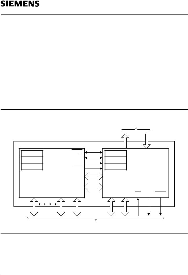
CPU
The C515A is efficient both as a controller and as an arithmetic processor. It has extensive facilities for binary and BCD arithmetic and excels in its bit-handling capabilities. Efficient use of program memory results from an instruction set consisting of 44 % one-byte, 41 % two-byte, and 15% three-byte instructions. With a 18 MHz crystal, 58% of the instructions are executed in 666 ns (24 MHz : 500 ns).
Special Function Register PSW (Address D0H) |
|
|
Reset Value : 00H |
||||||
Bit No. |
MSB |
|
|
|
|
|
|
LSB |
|
|
D7H |
D6H |
D5H |
D4H |
D3H |
D2H |
D1H |
D0H |
|
D0H |
CY |
AC |
F0 |
RS1 |
RS0 |
OV |
F1 |
P |
PSW |
Bit |
Function |
CY |
Carry Flag |
|
Used by arithmetic instruction. |
|
|
AC |
Auxiliary Carry Flag |
|
Used by instructions which execute BCD operations. |
|
|
F0 |
General Purpose Flag |
|
|
RS1 |
Register Bank select control bits |
RS0 |
These bits are used to select one of the four register banks. |
|
|
|
|
|
|
|
|
|
RS1 |
RS0 |
Function |
|
|
|
|
|
|
|
|
|
|
|
0 |
0 |
Bank 0 selected, data address 00H-07H |
|
|
|
|
0 |
1 |
Bank 1 selected, data address 08H-0FH |
|
|
|
|
1 |
0 |
Bank 2 selected, data address 10H-17H |
|
|
|
|
1 |
1 |
Bank 3 selected, data address 18H-1FH |
|
|
|
|
|
|
|
|
|
|
|
|
|
|
|
|
OV |
Overflow Flag |
|
|
|
||
|
Used by arithmetic instruction. |
|||||
|
|
|
|
|
|
|
F1 |
General Purpose Flag |
|
|
|
||
|
|
|
|
|
|
|
P |
Parity Flag |
|
|
|
|
|
|
Set/cleared by hardware after each instruction to indicate an odd/even |
|||||
|
number of “one” bits in the accumulator, i.e. even parity. |
|||||
Semiconductor Group |
13 |
1997-10-01 |
C515A
Memory Organization
The C515A CPU manipulates operands in the following five address spaces:
–up to 64 Kbyte of program memory (32K on-chip program memory for C515A-4R)
–up to 64 Kbyte of external data memory
–256 bytes of internal data memory
–1K bytes of internal XRAM data memory
–a 128 byte special function register area
Figure 5 illustrates the memory address spaces of the C515A.
|
|
Alternatively |
|
|
|
|
|
FFFF H |
|
|
FFFF H |
|
|
|
|
Ext. |
Internal |
|
|
|
|
|
Data |
XRAM |
|
|
|
|
|
Memory |
(1 KByte) |
|
|
|
|
Ext. |
|
|
FC00 H |
|
|
|
|
|
FBFF H |
|
|
|
|
|
|
|
Indirect |
Direct |
|
|
8000 H |
|
|
Addr. |
Addr. |
FF H |
|
|
|
|
|
||
|
|
7FFFH |
|
Internal |
Special |
|
|
|
Ext. |
|
RAM |
Function |
|
|
|
|
Regs. |
|
||
|
|
Data |
|
|
|
|
|
|
|
|
|
80 H |
|
Int. |
Ext. |
Memory |
|
|
|
|
|
|
|
7F H |
|
||
EA = 1) |
EA = 1) |
|
|
|
|
|
|
|
|
|
|
Internal |
|
|
|
|
|
|
RAM |
|
|
|
0000 H |
0000 H |
|
00 H |
|
"Code Space" |
"Data Space" |
"Internal Data Space" |
|
|||
|
|
|
|
|
MCB03243 |
|
Figure 5
C515A Memory Map
Semiconductor Group |
14 |
1997-10-01 |
C515A
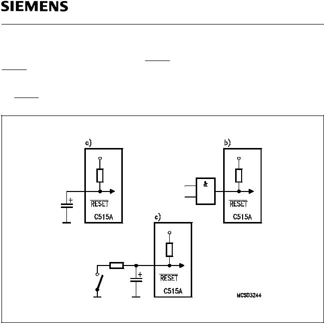
Reset and System Clock
The reset input is an active low input at pin RESET. Since the reset is synchronized internally, the RESET pin must be held low for at least two machine cycles (24 oscillator periods) while the oscillator is running. A pullup resistor is internally connected to VCC to allow a power-up reset with an external capacitor only. An automatic reset can be obtained when VCC is applied by connecting
the RESET pin to VSS via a capacitor. Figure 6 shows the possible reset circuitries.
Figure 6
Reset Circuitries
Semiconductor Group |
15 |
1997-10-01 |
C515A
Figure 7 shows the recommended oscillator circuitries for crystal and external clock operation.
|
|
Crystal Oscillator Mode |
Driving from External Source |
||||||||||||||
|
|
|
|
|
|
|
|
|
|||||||||
|
|
C |
|
N.C. |
|
||||||||||||
|
|
|
|
|
|
|
|
|
|
|
|
|
|
|
XTAL1 |
XTAL1 |
|
|
|
|
|
|
|
|
|
|
|
|
|
|
|
|
|||
|
|
|
|
|
|
|
|
|
|
|
|
|
|
|
|
||
|
|
|
|
|
|
|
|
|
|
|
|
|
|
|
|
||
|
|
3.5 - 24 |
|
|
|
|
|
|
|
|
|
|
|
|
|
||
|
|
MHz |
|
|
|
|
|
|
|
|
|
|
|
External Oscillator |
|
||
|
|
|
|
|
|
|
|
|
|
|
|
|
|
|
XTAL2 |
Signal |
XTAL2 |
|
|
|
|
|
|
|
|
|
|
|
|
|
|
|
|||
|
|
|
|
|
|
|
|
|
|
|
|
|
|
|
|
||
|
|
|
|
|
|
|
|
|
|
|
|
|
|
|
|
||
|
|
C |
|
|
|
||||||||||||
|
|
|
|
|
|
|
|
||||||||||
Crystal Mode: C = 20 pF |
|
|
|
10 pF |
|
|
|||||||||||
|
|
|
|
|
|
||||||||||||
|
|
|
|
(Incl. Stray Capacitance) |
|
MCS03245 |
|||||||||||
Figure 7
Recommended Oscillator Circuitries
Semiconductor Group |
16 |
1997-10-01 |
C515A
Enhanced Hooks Emulation Concept
The Enhanced Hooks Emulation Concept of the C500 microcontroller family is a new, innovative way to control the execution of C500 MCUs and to gain extensive information on the internal operation of the controllers. Emulation of on-chip ROM based programs is possible, too.
Each production chip has built-in logic for the support of the Enhanced Hooks Emulation Concept. Therefore, no costly bond-out chips are necessary for emulation. This also ensure that emulation and production chips are identical.
The Enhanced Hooks TechnologyTM 1), which requires embedded logic in the C500 allows the C500 together with an EH-IC to function similar to a bond-out chip. This simplifies the design and reduces costs of an ICE-system. ICE-systems using an EH-IC and a compatible C500 are able to emulate all operating modes of the different versions of the C500 microcontrollers. This includes emulation of ROM, ROM with code rollover and ROMless modes of operation. It is also able to operate in single step mode and to read the SFRs after a break.
|
|
|
ICE-System interface |
|
||
|
|
|
to emulation hardware |
|
||
SYSCON |
|
RESET |
RSYSCON |
|
|
|
|
EA |
|
|
|||
PCON |
|
RPCON |
|
EH-IC |
|
|
|
ALE |
|
|
|||
TCON |
|
RTCON |
|
|
|
|
|
PSEN |
|
|
|
||
|
|
|
|
|
|
|
|
C500 |
Port 0 |
|
Enhanced Hooks |
|
|
|
MCU |
|
|
Interface Circuit |
|
|
opt. |
|
Port 2 |
RPORT RPORT |
|
|
|
|
|
|
|
|||
I/O Ports |
Port 3 |
Port 1 |
2 |
0 |
TEA TALE |
TPSEN |
|
|
Target System Interface |
|
|
MCS03254 |
|
Figure 8
Basic C500 MCU Enhanced Hooks Concept Configuration
Port 0, port 2 and some of the control lines of the C500 based MCU are used by Enhanced Hooks Emulation Concept to control the operation of the device during emulation and to transfer informations about the program execution and data transfer between the external emulation hardware (ICE-system) and the C500 MCU.
1 “Enhanced Hooks Technology” is a trademark and patent of Metalink Corporation licensed to Siemens.
Semiconductor Group |
17 |
1997-10-01 |

C515A
Special Function Registers
The registers, except the program counter and the four general purpose register banks, reside in the special function register area. The special function register area consists of two portions: the standard special function register area and the mapped special function register area. One special function register of the C515A (PCON1) is located in the mapped special function register area. For accessing this mapped special function register, bit RMAP in special function register SYSCON must be set. All other special function registers are located in the standard special function register area which is accessed when RMAP is cleared (“0“).
Special Function Register SYSCON (Address B1H) |
|
|
Reset Value : XX10XX01B |
|||||||
Bit No. |
MSB |
|
|
|
|
|
|
|
LSB |
|
|
7 |
6 |
5 |
4 |
3 |
2 |
1 |
0 |
|
|
|
|
|
|
|
|
|
|
|
|
|
B1H |
– |
– |
EALE |
RMAP |
– |
– |
XMAP1 |
XMAP0 |
SYSCON |
|
|
The functions of the shaded bits are not described in this section. |
|||||||||
Bit |
Function |
|
|
RMAP |
Special function register map bit |
|
RMAP = 0: The access to the non-mapped (standard) special function |
|
register area is enabled. |
|
RMAP = 1: The access to the mapped special function register area (SFR |
|
PCON1) is enabled. |
|
|
– |
Reserved bits for future use. Read by CPU returns undefined values. |
|
|
As long as bit RMAP is set, the mapped special function register area (SFR PCON1) can be accessed. This bit is not cleared by hardware automatically. Thus, when non-mapped/mapped registers are to be accessed, the bit RMAP must be cleared/set respectively by software.
The 49 special function registers (SFRs) in the standard and mapped SFR area include pointers and registers that provide an interface between the CPU and the other on-chip peripherals. All SFRs with addresses where address bits 0-2 are 0 (e.g. 80H, 88H, 90H, 98H, …, F8 H, FFH) are bitaddressable. The SFRs of the C515A are listed in table 2 and table 3. In table 2 they are organized in groups which refer to the functional blocks of the C515A. Table 3 illustrates the contents of the SFRs in numeric order of their addresses.
Semiconductor Group |
18 |
1997-10-01 |
 Loading...