


Siemens SAB-C504-2R24M, SAB-C504-2R40M, SAB-C504-2RM, SAB-C504-L24M, SAB-C504-L40M Datasheet
...Microcomputer Components
8-Bit CMOS Microcontroller
C504
Data Sheet 05.96

C504 |
|
|
|
Revision History: |
|
Current Version: 05.96 |
|
|
|
|
|
Previous Version: |
|
|
|
|
|
|
|
Page |
Page |
|
Subjects (major changes since last revision) |
(in previous |
( i n |
n e w |
|
Version) |
Version) |
|
|
|
|
|
|
|
|
|
|
|
|
|
|
Edition 05.96
This edition was realized using the software system FrameMakerâ.
Published by Siemens AG, Bereich Halbleiter, MarketingKommunikation, Balanstraße 73, 81541 München
© Siemens AG 1996.
All Rights Reserved.
Attention please!
As far as patents or other rights of third parties are concerned, liability is only assumed for components, not for applications, processes and circuits implemented within components or assemblies.
The information describes the type of component and shall not be considered as assured characteristics. Terms of delivery and rights to change design reserved.
For questions on technology, delivery and prices please contact the Semiconductor Group Offices in Germany or the Siemens Companies and Representatives worldwide (see address list).
Due to technical requirements components may contain dangerous substances. For information on the types in question please contact your nearest Siemens Office, Semiconductor Group.
Siemens AG is an approved CECC manufacturer.
Packing
Please use the recycling operators known to you. We can also help you – get in touch with your nearest sales office. By agreement we will take packing material back, if it is sorted. You must bear the costs of transport.
For packing material that is returned to us unsorted or which we are not obliged to accept, we shall have to invoice you for any costs incurred.
Components used in life-support devices or systems must be expressly authorized for such purpose!
Critical components1 of the Semiconductor Group of Siemens AG, may only be used in life-support devices or systems2 with the express written approval of the Semiconductor Group of Siemens AG.
1A critical component is a component used in a life-support device or system whose failure can reasonably be expected to cause the failure of that life-support device or system, or to affect its safety or effectiveness of that device or system.
2Life support devices or systems are intended (a) to be implanted in the human body, or (b) to support and/or maintain and sustain human life. If they fail, it is reasonable to assume that the health of the user may be endangered.

8-Bit CMOS Microcontroller |
C504 |
Advance Information
• Fully compatible to standard 8051 microcontroller |
|
|||
• Up to 40 MHz operating frequency |
|
|
|
|
• 16 K×8 ROM (C504-2R only, optional ROM protection) |
|
|||
• 256×8 RAM |
|
|
|
|
• 256×8 XRAM |
|
|
|
|
• Four 8-bit ports, (2 ports with mixed analog/digital I/O capability) |
|
|||
• Three 16-bit timers/counters (timer 2 with up/down counter feature) |
|
|||
• Capture/compare unit for PWM signal generation and signal capturing |
|
|||
- |
3-channel, 16-bit capture/compare unit |
|
|
|
- |
1-channel, 10-bit compare unit |
|
|
|
• Compare unit |
|
|
|
|
• USART |
|
|
|
|
• 10-bit A/D Converter with 8 multiplexed inputs |
|
|||
• Twelve interrupt sources with two priority levels |
|
|||
• On-chip emulation support logic (Enhanced Hooks Technology TM) |
|
|||
• Programmable 15-bit Watchdog Timer |
|
|
||
• Oscillator Watchdog |
|
|
|
|
• Fast Power On Reset |
|
|
|
|
• Power Saving Modes |
|
|
|
|
• M-QFP-44 package |
|
0 to 70°C |
|
|
• Temperature ranges: SAB-C504 |
TA : |
|
||
|
SAF-C504 |
TA : – 40 to 85°C |
|
|
|
SAH-C504 |
TA : – 40 to 110°C (max. operating frequency.: TBD) |
||
|
SAK-C504 |
TA : – 40 to 125°C (max. operating frequency.: 12 MHz) |
||
Semiconductor Group |
|
3 |
05.96 |
|

C504
The C504 with its capture compare unit (CCU) especially provides a functionality, which allows to use the microcontroller in motor control applications. Further, the C504 is functionally upward compatible with the SAB 80C52/C501 microcontroller and can replace it in existing applications.
The C504-2R contains a non-volatile 16K×8 read-only program memory, a volatile on-chip 512×8 read/write data memory, four 8-bit wide ports, three 16-bit timers/counters, a 16-bit capture/ compare unit with compare timer, a 10-bit compare timer, a twelve source, two priority level interrupt structure, a serial port, versatile fail save mechanisms, on-chip emulation support logic, and a genuine 10-bit A/D converter. The C504-L is identical to the C504-2R, except that it lacks the program memory on chip. Therefore, the term C504 refers to all versions within this data sheet unless otherwise noted.
Ordering Information
Type |
Ordering Code |
Package |
Description |
|
|
|
(8-Bit CMOS microcontroller) |
|
|
|
|
SAB-C504-LM |
Q67120-C1048 |
P-MQFP-44 |
for external memory (12 MHz) |
|
|
|
|
SAB-C504-L24M |
Q67120-C1049 |
P-MQFP-44 |
for external memory (24 MHz) |
|
|
|
|
SAB-C504-L40M |
Q67120-C1050 |
P-MQFP-44 |
for external memory (40 MHz) |
|
|
|
|
SAB-C504-2RM |
Q67120-DXXXX |
P-MQFP-44 |
with mask-programmable ROM (12 MHz) |
|
|
|
|
SAB-C504-2R24M |
Q67120-DXXXX |
P-MQFP-44 |
with mask-programmable ROM (24 MHz) |
|
|
|
|
SAB-C504-2R40M |
Q67120-DXXXX |
P-MQFP-44 |
with mask-programmable ROM (40 MHz) |
|
|
|
|
Note: Versions for extended temperature ranges – 40 ˚C to 110 ˚C (SAH-C504) and – 40 ˚C to 125 ˚C (SAK-C504) are available on request.
The ordering number of ROM types (DXXXX extensions) is defined after program release (verification) of the customer.
Semiconductor Group |
4 |
C504
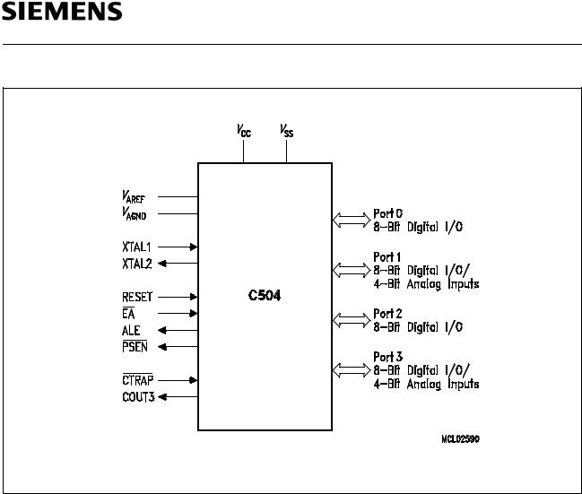
Figure 1
Logic Symbol
Semiconductor Group |
5 |

C504 |
Figure 2
Pin Configuration (top view)
Semiconductor Group |
6 |

C504
Table 1
Pin Definitions and Functions
Symbol |
Pin Number |
I/O |
Function |
|
|
|
(P-MQFP-44) |
*) |
|
|
|
|
|
|
|
|
|
P1.0-P1.7 |
40-44, |
I/O |
Port 1 |
|
|
|
1-3 |
|
is an 8-bit bidirectional port. Port pins can be used for |
||
|
|
|
digital input/output. P1.0 - P1.3 can also be used as analog |
||
|
|
|
inputs of the A/D-converter. As secondary digital functions, |
||
|
|
|
port 1 contains the timer 2 pins and the capture/compare |
||
|
|
|
inputs/outputs. Port 1 pins are assigned to be used as |
||
|
|
|
analog inputs via the register P1ANA. |
||
|
|
|
The functions are assigned to the pins of port 1 as follows: |
||
|
40 |
|
P1.0 |
/ AN0 / T2 |
Analog input channel 0 / |
|
|
|
|
|
input to counter 2 |
|
41 |
|
P1.1 |
/ AN1 / T2EX |
Analog input channel 1 / |
|
|
|
|
|
capture/reload trigger of timer 2 / |
|
|
|
|
|
up-down count |
|
42 |
|
P1.2 |
/ AN2 / CC0 |
Analog input channel 2 / |
|
|
|
|
|
input/output of capture/compare |
|
|
|
|
|
channel 0 |
|
43 |
|
P1.3 |
/ AN3 / COUT0 |
Analog input channel 3 / |
|
|
|
|
|
output of capture/compare |
|
|
|
|
|
channel 0 |
|
44 |
|
P1.4 |
/ CC1 |
Input/output of capture/compare |
|
|
|
|
|
channel 1 |
|
1 |
|
P1.5 |
/ COUT1 |
Output of capture/compare |
|
|
|
|
|
channel 1 |
|
2 |
|
P1.6 |
/ CC2 |
Input/output of capture/compare |
|
|
|
|
|
channel 2 |
|
3 |
|
P1.7 |
/ COUT2 |
Output of capture/compare |
|
|
|
|
|
channel 2 |
|
|
|
|
|
|
RESET |
4 |
I |
RESET |
|
|
|
|
|
A high level on this pin for one machine cycle while the |
||
|
|
|
oscillator is running resets the device. An internal diffused |
||
|
|
|
resistor to VSS permits power-on reset using only an |
||
|
|
|
external capacitor to VCC. |
||
|
|
|
|
|
|
*) I = Input |
|
|
|
|
|
O = Output |
|
|
|
|
|
Semiconductor Group |
7 |

C504
Table 1
Pin Definitions and Functions (cont’d)
Symbol |
Pin Number |
I/O |
|
Function |
|
|
||||||||||||
|
|
(P-MQFP-44) |
*) |
|
|
|
|
|
|
|
|
|
|
|
|
|
|
|
|
|
|
|
|
|
|
||||||||||||
P3.0-P3.7 |
5, 7-13 |
I/O |
|
Port 3 |
|
|
||||||||||||
|
|
|
|
|
is an 8-bit bidirectional port. P3.0 (R×D) and P3.1 (T×D) |
|||||||||||||
|
|
|
|
|
operate as defined for the C501. P3.2 to P3.7 contain the |
|||||||||||||
|
|
|
|
|
external interrupt inputs, timer inputs, input and as an |
|||||||||||||
|
|
|
|
|
additional optinal function four of the analog inputs of the |
|||||||||||||
|
|
|
|
|
A/D-converter. Port 3 pins are assigned to be used as |
|||||||||||||
|
|
|
|
|
analog inputs via the bits of SFR P3ANA. |
|||||||||||||
|
|
|
|
|
|
|
|
|
|
can be assigned as a third interrupt input. The |
||||||||
|
|
|
|
|
P3.6/WR |
|||||||||||||
|
|
|
|
functions are assigned to the pins of port 3 as follows: |
||||||||||||||
|
|
5 |
|
P3.0 / RxD |
Receiver data input (asynch.) or data |
|||||||||||||
|
|
|
|
|
|
|
|
|
|
|
|
|
|
|
|
|
input/output (synch.) of serial |
|
|
|
|
|
|
|
|
|
|
|
|
|
|
|
|
|
|
interface |
|
|
|
7 |
|
P3.1 / TxD |
Transmitter data output (asynch.) or |
|||||||||||||
|
|
|
|
|
|
|
|
|
|
|
|
|
|
|
|
|
clock output (synch.) of serial |
|
|
|
|
|
|
|
|
|
|
|
|
|
|
|
|
|
|
interface |
|
|
|
8 |
|
P3.2 / AN4 / |
INT0 |
|
Analog input channel 4 / external |
|||||||||||
|
|
|
|
|
|
|
|
|
|
|
|
|
|
|
|
|
interrupt 0 input / timer 0 gate control |
|
|
|
|
|
|
|
|
|
|
|
|
|
|
|
|
|
|
input |
|
|
|
9 |
|
|
P3.3 / AN5 / |
INT1 |
|
Analog input channel 5 / external |
||||||||||
|
|
|
|
|
|
|
|
|
|
|
|
|
|
|
|
|
interrupt 1 input / timer 1 gate control |
|
|
|
|
|
|
|
|
|
|
|
|
|
|
|
|
|
|
input |
|
|
|
10 |
|
|
P3.4 / AN6 / T0 |
Analog input channel 6 / timer 0 |
||||||||||||
|
|
|
|
|
|
|
|
|
|
|
|
|
|
|
|
|
counter input |
|
|
|
11 |
|
|
P3.5 / AN7 / T1 |
Analog input channel 7 / timer 1 |
||||||||||||
|
|
|
|
|
|
|
|
|
|
|
|
|
|
|
|
|
counter input |
|
|
|
|
|
|
|
|
|
|
|
|
|
|
|
|
||||
|
|
12 |
|
|
P3.6 / |
WR |
/ |
INT2 |
|
WR |
control output; latches the data |
|||||||
|
|
|
|
|
|
|
|
|
|
|
|
|
|
|
|
|
byte from port 0 into the external data |
|
|
|
|
|
|
|
|
|
|
|
|
|
|
|
|
|
|
memory / |
|
|
|
|
|
|
|
|
|
|
|
|
|
|
|
|
|
|
external interrupt 2 input |
|
|
|
13 |
|
|
P3.7 / |
RD |
|
|
|
RD |
control output; enables the |
|||||||
|
|
|
|
|
|
|
|
|
|
|
|
|
|
|
|
|
external data memory |
|
|
|
|
|
|
|
|
|
|
|
|
|
|||||||
|
|
6 |
I |
|
|
|
|
|
|
|
|
|
|
|
|
|
|
|
CTRAP |
|
CCU Trap Input |
|
|
||||||||||||||
|
|
|
|
|
With |
CTRAP |
= low the compare outputs of the CAPCOM |
|||||||||||
|
|
|
|
unit are switched to the logic level as defined in the COINI |
||||||||||||||
|
|
|
|
register (if they are enabled by the bits in SFR TRCON). |
||||||||||||||
|
|
|
|
|
CTRAP |
|
is an input pin with an internal pullup resistor. For |
|||||||||||
|
|
|
|
|
power saving reasons, the signal source which drives the |
|||||||||||||
|
|
|
|
|
CTRAP |
input should be at high or floating level during |
||||||||||||
|
|
|
|
|
power-down mode. |
|
|
|||||||||||
|
|
|
|
|
|
|
|
|
|
|
|
|
|
|
|
|
|
|
*) I = Input |
|
|
|
|
|
|
|
|
|
|
|
|
|
|
|
|
|
|
O = Output |
|
|
|
|
|
|
|
|
|
|
|
|
|
|
|
|
|
|
Semiconductor Group |
8 |

C504
Table 1
Pin Definitions and Functions (cont’d)
Symbol |
Pin Number |
I/O |
Function |
||||
|
|
(P-MQFP-44) |
*) |
|
|
|
|
|
|
|
|
||||
XTAL2 |
14 |
– |
XTAL2 |
||||
|
|
|
|
Output of the inverting oscillator amplifier. |
|||
|
|
|
|
||||
XTAL1 |
15 |
– |
XTAL1 |
||||
|
|
|
|
Input to the inverting oscillator amplifier and input to the |
|||
|
|
|
|
internal clock generator circuits. |
|||
|
|
|
|
To drive the device from an external clock source, XTAL1 |
|||
|
|
|
|
should be driven, while XTAL2 is left unconnected. There |
|||
|
|
|
|
are no requirements on the duty cycle of the external clock |
|||
|
|
|
|
signal, since the input to the internal clocking circuitry is |
|||
|
|
|
|
divided down by a divide-by-two flip-flop. Minimum and |
|||
|
|
|
|
maximum high and low times as well as rise/fall times |
|||
|
|
|
|
specified in the AC characteristics must be observed. |
|||
|
|
|
|
||||
P2.0-P2.7 |
18-25 |
I/O |
Port 2 |
||||
|
|
|
|
is a bidirectional I/O port with internal pullup resistors. Port |
|||
|
|
|
|
2 pins that have 1s written to them are pulled high by the |
|||
|
|
|
|
internal pullup resistors, and in that state can be used as |
|||
|
|
|
|
inputs. As inputs, port 2 pins being externally pulled low |
|||
|
|
|
|
will source current (IIL, in the DC characteris-tics) because |
|||
|
|
|
|
of the internal pullup resistors. Port 2 emits the high-order |
|||
|
|
|
|
address byte during fetches from external program |
|||
|
|
|
|
memory and during accesses to external data memory that |
|||
|
|
|
|
use 16-bit addresses (MOVX @DPTR). In this application |
|||
|
|
|
|
it uses strong internal pullup resistors when issuing 1s. |
|||
|
|
|
|
During accesses to external data memory that use 8-bit |
|||
|
|
|
|
addresses (MOVX @Ri), port 2 issues the contents of the |
|||
|
|
|
|
P2 special function register. |
|||
|
|
|
|
|
|
|
|
|
|
26 |
O |
The |
|
|
|
PSEN |
|
Program Store Enable |
|||||
|
|
|
|
output is a control signal that enables the external program |
|||
|
|
|
|
memory to the bus during external fetch operations. It is |
|||
|
|
|
|
activated every six oscillator periodes except during |
|||
|
|
|
|
external data memory accesses. Remains high during |
|||
|
|
|
|
internal program execution. |
|||
|
|
|
|
||||
ALE |
27 |
O |
The Address Latch Enable |
||||
|
|
|
|
output is used for latching the low-byte of the address into |
|||
|
|
|
|
external memory during normal operation. It is activated |
|||
|
|
|
|
every six oscillator periodes except during an external data |
|||
|
|
|
|
memory access. When instructions are executed from |
|||
|
|
|
|
internal ROM |
(EA=1) the ALE generation can be disabled |
||
|
|
|
|
by bit EALE in SFR SYSCON. |
|||
|
|
|
|
|
|
|
|
*) I = Input |
|
|
|
|
|
|
|
O = Output |
|
|
|
|
|
|
|
Semiconductor Group |
9 |

C504
Table 1
Pin Definitions and Functions (cont’d)
Symbol |
Pin Number |
I/O |
|
Function |
||
|
|
(P-MQFP-44) |
*) |
|
|
|
|
|
|
|
|
||
COUT3 |
28 |
O |
|
10-Bit compare channel output |
||
|
|
|
|
|
This pin is used for the output signal of the 10-bit compare |
|
|
|
|
|
|
timer 2 unit. COUT3 can be disabled and set to a high or |
|
|
|
|
|
|
low state. |
|
|
|
|
|
|
|
|
|
|
29 |
I |
|
|
Enable |
EA |
|
|
External Access |
|||
|
|
|
|
|
When held at high level, instructions are fetched from the |
|
|
|
|
|
|
internal ROM (C504-2R only) when the PC is less than |
|
|
|
|
|
|
4000H.When held at low level, the C504 fetches all |
|
|
|
|
|
|
instructions from external program memory. |
|
|
|
|
|
|
For the C504-L this pin must be tied low. |
|
|
|
|
|
|
||
P0.0-P0.7 |
37-30 |
I/O |
|
Port 0 |
||
|
|
|
|
|
is an 8-bit open-drain bidirectional I/O port. Port 0 pins that |
|
|
|
|
|
|
have 1s written to them float, and in that state can be used |
|
|
|
|
|
|
as high-impendance inputs.Port 0 is also the multiplexed |
|
|
|
|
|
|
low-order address and data bus during accesses to |
|
|
|
|
|
|
external program or data memory. In this application it |
|
|
|
|
|
|
uses strong internal pullup resistors when issuing 1 s. |
|
|
|
|
|
|
Port 0 also outputs the code bytes during program |
|
|
|
|
|
|
verification in the C504-2R. External pullup resistors are |
|
|
|
|
|
|
required during program (ROM) verification. |
|
|
|
|
|
|
||
VAREF |
38 |
– |
|
Reference voltage for the A/D converter. |
||
VAGND |
39 |
– |
|
Reference ground for the A/D converter. |
||
VSS |
16 |
– |
|
Ground (0V) |
||
VCC |
17 |
– |
|
Power Supply (+5V) |
||
*) I = Input |
|
|
|
|
|
|
|
O = Output |
|
|
|
|
|
Semiconductor Group |
10 |

C504
Functional Description
The C504 basic architecture is fully compatible to the standard 8051 microcontroller family. While maintaining all architectural and operational characteristics of the SAB 80C52 / C501, the C504 incorporates some enhancements such as on-chip XRAM, A/D converter, fail save mechanisms, and a versatile capture/compare unit.
Figure 3 shows a block diagram of the C504.
Figure 3
Block Diagram of the C504
Semiconductor Group |
11 |

C504
CPU
The C504 is efficient both as a controller and as an arithmetic processor. It has extensive facilities for binary and BCD arithmetic and excels in its bit-handling capabilities. Efficient use of program memory results from an instruction set consisting of 44 % one-byte, 41 % two-byte, and 15 % threebyte instructions. With a 12 MHz crystal, 58 % of the instructions are executed in 1.0μs (24 MHz: 500 ns, 40 MHz : 300 ns).
Special Function Register PSW (Address D0H) |
|
|
Reset Value : 00H |
||||||
Bit No. |
MSB |
|
|
|
|
|
|
LSB |
|
|
D7H |
D6H |
D5H |
D4H |
D3H |
D2H |
D1H |
D0H |
|
D0H |
CY |
AC |
F0 |
RS1 |
RS0 |
OV |
F1 |
P |
PSW |
Bit |
Function |
CY |
Carry Flag |
|
Used by arithmetic instruction. |
|
|
AC |
Auxiliary Carry Flag |
|
Used by instructions which execute BCD operations. |
|
|
F0 |
General Purpose Flag |
|
|
RS1 |
Register Bank select control bits |
RS0 |
These bits are used to select one of the four register banks. |
|
|
RS1 |
RS0 |
Function |
|
|
|
|
|
|
|
|
|
0 |
0 |
Bank 0 selected, data address 00H-07H |
|
|
|
0 |
1 |
Bank 1 selected, data address 08H-0FH |
|
|
|
1 |
0 |
Bank 2 selected, data address 10H-17H |
|
|
1 |
1 |
Bank 3 selected, data address 18H-1FH |
||
|
|
|
|
|
|
OV |
Overflow Flag |
|
|
||
|
Used by arithmetic instruction. |
||||
|
|
|
|
|
|
F1 |
General Purpose Flag |
|
|
||
|
|
|
|
|
|
P |
Parity Flag |
|
|
|
|
|
Set/cleared by hardware after each instruction to indicate an odd/even |
||||
|
number of "one" bits in the accumulator, i.e. even parity. |
||||
Semiconductor Group |
12 |

C504
Memory Organization
The C504 CPU manipulates operands in the following four address spaces:
–up to 64 Kbyte of external program memory
–up to 64 Kbyte of external data memory
–256 bytes of internal data memory
–256 bytes of internal XRAM data memory
–a 128 byte special function register area
Figure 4 illustrates the memory address spaces of the C504.
Figure 4
C504 Memory Map
The XRAM in the C504 is a memory area that is logically located at the upper end of the external memory space, but is integrated on the chip. Because the XRAM is used in the same way as external data memory the same instruction types (MOVX instructions) must be used for accessing the XRAM. The XRAM can be enabled and disabled by the XMAP bit in the SYSCON register.
ROM Protection
The C504-2R ROM version allows to protect the content of the internal ROM against read out by non authorized people. The type of ROM protection (protected or unprotected) is fixed with the ROM mask. Therefore, the customer of a C504-2R ROM version has to define whether ROM protection has to be selected or not.
Semiconductor Group |
13 |

C504
Special Function Registers
All registers, except the program counter and the four general purpose register banks, reside in the special function register area.
The 63 special function register (SFR) include pointers and registers that provide an interface between the CPU and the other on-chip peripherals. There are also 128 directly addressable bits within the SFR area.
The SFRs of the C504 are listed in table 2 and table 3. In table 2 they are organized in groups which refer to the functional blocks of the C504. Table 3 illustrates the contents of the SFRs in numeric order of their addresses.
Semiconductor Group |
14 |

C504
Table 2
Special Function Registers - Functional Blocks
Block |
Symbol |
Name |
Address |
Contents after |
||||||||
|
|
|
|
|
|
Reset |
|
|
|
|
||
|
|
|
|
|
|
|
|
|
|
|||
CPU |
ACC |
Accumulator |
E0H 1) |
00H |
|
|
|
|
|
|||
|
B |
B-Register |
F0H 1) |
00H |
|
|
|
|
|
|||
|
DPH |
Data Pointer, High Byte |
83H |
|
00H |
|
|
|
|
|
||
|
DPL |
Data Pointer, Low Byte |
82H |
|
00H |
|
|
|
|
|
||
|
PSW |
Program Status Word Register |
D0H 1) |
00H |
|
|
|
|
|
|||
|
SP |
Stack Pointer |
81H |
|
07H |
|
|
|
|
|
||
|
SYSCON |
System Control Register |
B1 |
|
|
XX10XXX0 |
|
3) |
||||
|
|
|
H |
|
|
|
|
|
B |
|
||
Interrupt |
IEN0 |
Interrupt Enable Register 0 |
A8H1) |
0X000000B 3) |
||||||||
System |
IEN1 |
Interrupt Enable Register 1 |
A9 |
|
|
XX000000 |
B |
3) |
||||
|
|
|
H |
|
|
|
|
|
|
|
||
|
CCIE 2) |
Capture/Compare Interrupt Enable Reg. |
D6 |
H |
|
00 |
|
|
|
|
|
|
|
|
|
|
|
H |
|
|
|
|
|
||
|
IP0 |
Interrupt Priority Register 0 |
B8H 1) |
XX000000B 3) |
||||||||
|
IP1 |
Interrupt Priority Register 1 |
B9 |
|
|
XX000000 |
B |
3) |
||||
|
|
|
H |
|
|
|
|
|
|
|
||
|
ITCON |
Interrupt Trigger Condition Register |
9AH |
|
00101010B |
|
|
|||||
Ports |
P0 |
Port 0 |
80H 1) |
FFH |
|
|
|
|
|
|||
|
P1 |
Port 1 |
90H 1) |
FFH |
|
|
|
|
|
|||
|
P1ANA 2) |
Port 1 Analog Input Selection Register |
90 |
|
1) 4) |
XXXX1111 |
|
3) |
||||
|
|
|
H |
|
|
|
|
|
B |
|
||
|
P2 |
Port 2 |
A0H 1) |
FFH |
|
|
|
|
|
|||
|
P3 |
Port 3 |
B0H 1) |
FFH |
|
|
|
|
|
|||
|
P3ANA 2) |
Port 3 Analog Input Selection Register |
B0 |
H |
1) 4) |
XX1111XX |
|
3) |
||||
|
|
|
|
|
|
|
|
|
B |
|
||
A/D- |
ADCON0 |
A/D Converter Control Register 0 |
D8H 1 |
XX000000B 3) |
||||||||
Converter |
ADCON1 |
A/D Converter Control Register 1 |
DCH |
01XXX000B 3) |
||||||||
|
ADDATH |
A/D Converter Data Register High Byte |
D9H |
|
00H |
|
|
|
|
|
||
|
ADDATL |
A/D Converter Data Register Low Byte |
DAH |
00XXXXXXB 3) |
||||||||
|
P1ANA 2) |
Port 1 Analog Input Selection Register |
90 |
|
4) |
XXXX1111 |
|
3) |
||||
|
|
|
H |
|
|
|
|
|
B |
|
||
|
P3ANA 2) |
Port 3 Analog Input Selection Register |
B0 |
|
4) |
XX1111XX |
|
3) |
||||
|
|
|
H |
|
|
|
|
|
B |
|
||
Serial |
PCON 2) |
Power Control Register |
87 |
|
|
000X0000 |
B |
|
|
|||
|
|
|
H |
|
|
|
|
|
|
|||
Channels |
SBUF |
Serial Channel Buffer Register |
99 |
|
|
XX |
H |
3) |
|
|
|
|
|
|
|
H |
|
|
|
|
|
|
|
||
|
SCON |
Serial Channel Control Register |
98H 1) |
00H |
|
|
|
|
|
|||
Timer 0/ |
TCON |
Timer 0/1 Control Register |
88H 1) |
00H |
|
|
|
|
|
|||
Timer 1 |
TH0 |
Timer 0, High Byte |
8CH |
|
00H |
|
|
|
|
|
||
|
TH1 |
Timer 1, High Byte |
8DH |
|
00H |
|
|
|
|
|
||
|
TL0 |
Timer 0, Low Byte |
8AH |
|
00H |
|
|
|
|
|
||
|
TL1 |
Timer 1, Low Byte |
8BH |
|
00H |
|
|
|
|
|
||
|
TMOD |
Timer Mode Register |
89H |
|
00H |
|
|
|
|
|
||
1)Bit-addressable special function registers
2)This special function register is listed repeatedly since some bits of it also belong to other functional blocks.
3)X means that the value is undefined and the location is reserved
4)SFR is located in the mapped SFR area. For accessing this SFR, bit RMAP in SFR SYSCON must be set.
Semiconductor Group |
15 |
 Loading...