


SAB-C513-1RN
Siemens SAB-C513-1RN, SAB-C513A-2RM, SAB-C513A-2RN, SAB-C513A-LM, SAB-C513A-LN Datasheet
...
Data Sheet 06.96
Microcomputer Components
C51 1/C511A
C51 3/C51 3A
C51 3A-H
8-Bit CMOS Microcontroller

Data Sheet C511/C511A/C513/C513A/C513A-H
Revision History : Current Version : 06.96
Previous Releases : 02.96, 05.95
Page Subjects (changes since last revision)
Several
41
Corrections of text
Figure 22: external clock configuration corrected
8-Bit CMOS Microcontroller Family
Preliminary
C511
C511A
C513
C513A
C513A-H
●
Fully software compatible to standard 8051/8052 microcontrollers
●
Up to 12 MHz operating frequency
● Up to 12 K×8 ROM / EEPROM
●
Up to 256×8 RAM
●
Up to 256 x 8 XRAM
●
Four 8-bit ports
●
Up to three 16-bit Timers / Counters (Timer 2 with Up/Down and 16-bit Autoreload Feature)
●
Synchronous Serial Channel (SSC)
●
Optional USART
● Up to seven interrupt sources, two priority levels
●
Power Saving Modes
●
P-LCC-44 package (C513A also in P-MQFP-44 package)
●
Temperature Ranges : SAB-C511 / 511A / 513 / 513A / C513A-H
T
A
: 0 ˚C to 70 ˚C
SAF-C513A
T
A
: -40 ˚C to 85 ˚C
Semiconductor Group 3 06.96
Semiconductor Group 4
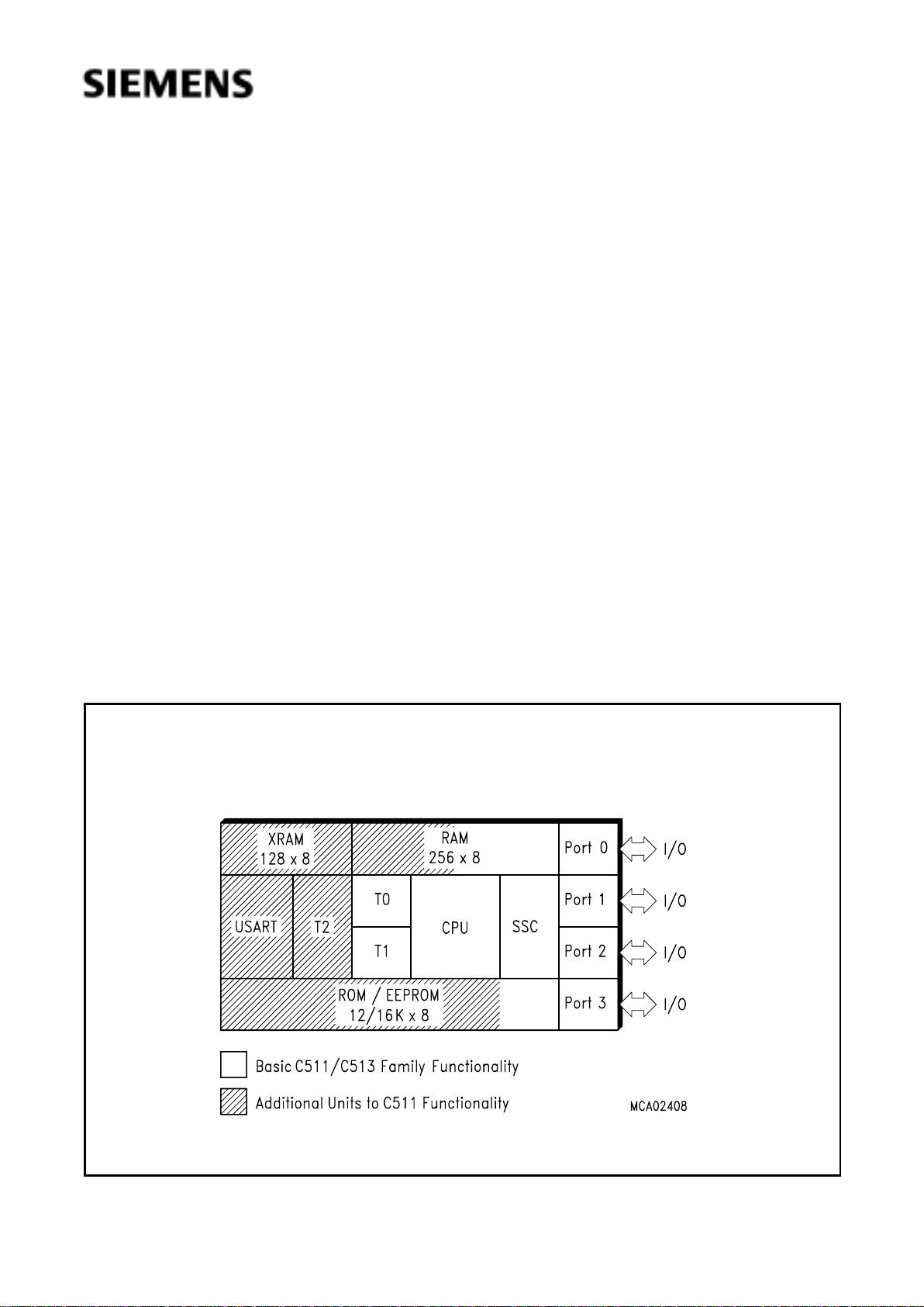
C511 / C513
The C511, C511A, C513, C513A, and C513A-H are members of a family of low cost microcontrollers, which are software compatible with the components of the SAB 8051, SAB 80C51 and
C500 families.
The first four versions contains a non-volatile read-only (ROM) program memory. The C513A-H is
a version with a 12 Kbyte EEPROM instead of ROM. This device can be used for prototype designs
which have a demand for reprogrammable on-chip code memory.
The members of the microcontroller family differ in functionality according table 1. They offer
different ROM sizes, different RAM/XRAM sizes and a different timer/USART configuration.
Common to all devices is an advanced SSC serial port, a second synchronous serial interface,
which is compatible to the SPI serial bus industry standard. The functionality of the C513A-H is a
superset of all ROM versions of the C511/C513 family.
Table 1
Functionality of the C511/C513 MCUs
1)
T0/T1 refers to the standard 8051 timer 0/1 units, T2 refers to the 8052 timer 2 unit.
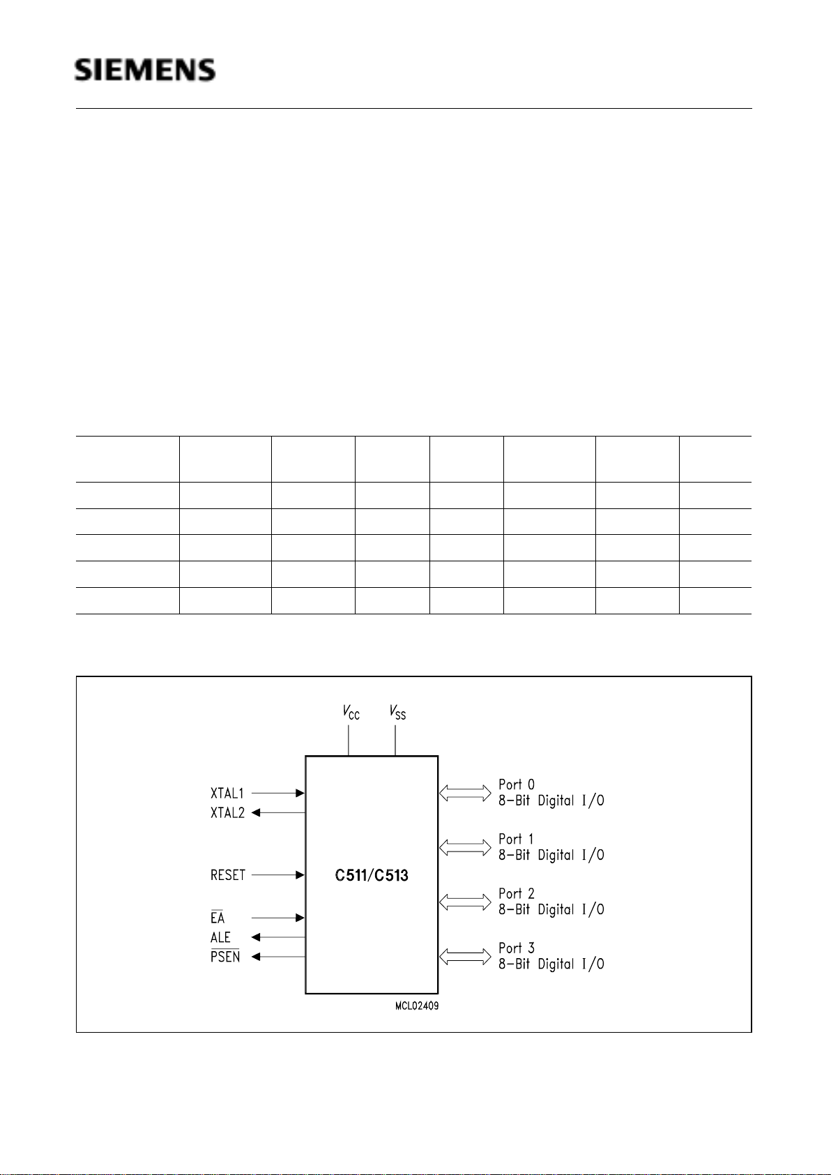
Figure 1
C511/513 Logic Symbol
Device ROM Size EEPROM
Size
RAM
Size
XRAM
Size
Timers
1)
USART SSC
C511 2.5 KB – 128 B – T0, T1 – ✓
C511A 4 KB – 256 B – T0, T1 – ✓
C513 8 KB – 256 B – T0, T1, T2 ✓✓
C513A 12, 16 KB – 256 B 256 B T0, T1, T2 ✓✓
C513A-H – 12 KB 256 B 256 B T0, T1, T2 ✓✓
C511 / C513
Semiconductor Group 5
Table 2
Ordering Information
Note : The ordering number of the ROM types (DXXXX extension) is defined after program release
(verification) of the customer.
Type Ordering
Code
Package Description
(8-Bit CMOS microcontroller)
C511-RN Q67120-DXXXX P-LCC-44 with mask-programmable ROM (2.5K), 12 MHz
C511A-RN Q67120-DXXXX P-LCC-44 with mask-programmable ROM (4K), 12 MHz
C513-1RN Q67120-DXXXX P-LCC-44 with mask-programmable ROM (8K), 12 MHz
C513A-RN Q67120-DXXXX P-LCC-44 with mask-programmable ROM (12K), 12 MHz
Q67120-DXXXX P-LCC-44 with mask-programmable ROM (12K), 12 MHz,
ext. temp. – 40 ˚C to 85 ˚C
C513A-2RN Q67120-DXXXX P-LCC-44 with mask-programmable ROM (16K), 12 MHz
Q67120-DXXXX P-LCC-44 with mask-programmable ROM (16K), 12 MHz,
ext. temp. – 40 ˚C to 85 ˚C
C513A-2RM Q67120-DXXXX P-MQFP-44 with mask-programmable ROM (16K), 12 MHz
Q67120-DXXXX P-MQFP-44 with mask-programmable ROM (16K), 12 MHz,
ext. temp. – 40 ˚C to 85 ˚C
C513A-LN Q67120-C1017 P-LCC-44 for external memory (12 MHz)
Q67120-C1035 P-LCC-44 for external memory (12 MHz),
ext. temp. – 40 ˚C to 85 ˚C
C513A-LM Q67120-C1026 P-MQFP-44 for external memory (12 MHz)
Q67120-C1036 P-MQFP-44 for external memory (12 MHz),
ext. temp. – 40 ˚C to 85 ˚C
C513A-HN Q67120-C0989 P-LCC-44 with reprogrammable EEPROM (12K), 12 MHz,
ext. temp. – 40 ˚C to 85 ˚C
Semiconductor Group 6
C511 / C513
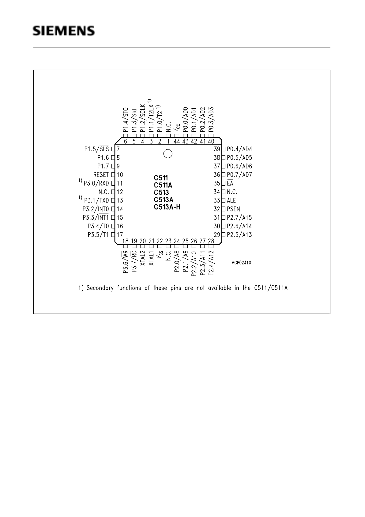
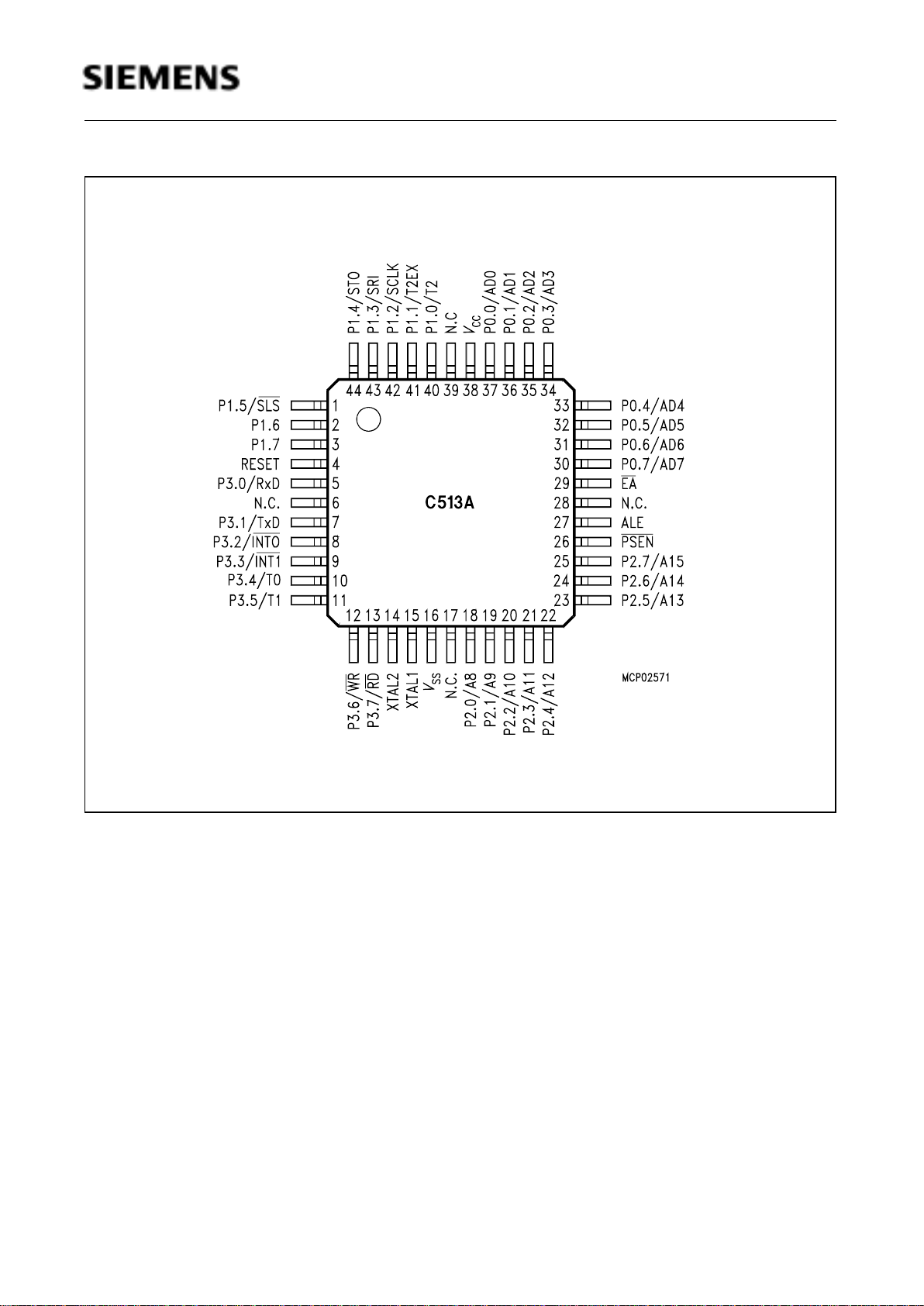
Figure 2
P-LCC-44 Package Pin Configuration (Top View)
If the C513A-H is used in programming mode, the pin configuration is different to figure 2 and 3 (see
figure 5).
C511 / C513
Semiconductor Group 7
Figure 3
P-MQFP-44 Package Pin Configuration of the C513A (Top View)
Semiconductor Group 8
C511 / C513
Table 3
Pin Definitions and Functions
Symbol Pin Number I/O*) Function
P-LCC-44P-MQFP-
44
P1.7-P1.0 9-2
2
3
4
5
6
7
3-1,
44-40
40
41
42
43
44
1
I/O Port 1
is a bidirectional I/O port with internal pull-up resistors.
Port 1 pins that have 1s written to them are pulled high by
the internal pullup resistors, and in that state can be used
as inputs. As inputs, port 1 pins being externally pulled
low will source current (
I
IL
, in the DC characteristics)
because of the internal pullup resistors. Port 1 also
contains the timer 2 and SSC pins as secondary function.
In general the output latch corresponding to a secondary
function must be programmed to a one (1) for that
function to operate.
For the outputs of the SSC (SCLK, STO) special circuitry
is implemented, providing true push-pull capability. The
STO output in addition will have true tristate capability.
When used for SSC inputs, the pull-up resistors will be
switched off and the inputs will float (high ohmic inputs).
The alternate functions are assigned to port 1, as follows:
P1.0 T2 Input to counter 2
1)
P1.1 T2EX Capture -Reload trigger of timer 2
1)
Up-Down count
P1.2 SCLK SSC Master Clock Output
SSC Slave Clock Input
P1.3 SRI SSC Receive Input
P1.4 STO SSC Transmit Output
P1.5 SLS
Slave Select Input
1
)
not available in the C511/511A
*) I = Input
O = Output
C511 / C513
Semiconductor Group 9
P3.0-P3.7 11,
13-19
11
13
14
15
16
17
18
19
5, 7-13
5
7
8
9
10
11
12
13
I/O Port 3
is a bidirectional I/O port with internal pull-up resistors.
Port 3 pins that have 1s written to them are pulled high by
the internal pullup resistors, and in that state can be used
as inputs. As inputs, port 3 pins being externally pulled
low will source current (I
IL
, in the DC characteristics)
because of the internal pullup resistors. Port 3 also
contains the interrupt, timer, serial port and external
memory strobe pins that are used by various options. The
output latch corresponding to a secondary function must
be programmed to a one (1) for that function to operate.
The secondary functions are assigned to the pins of port
3 as follows:
P3.0 RXD Receiver data input (asynchronous)
or data input/output (synchronous)
of serial interface (USART)
1)
P3.1 TXD Transmitter data output (USART)
1)
(asynchronous) or clock output
(synchronous) of serial interface
P3.2 INT0
Interrupt 0 input / timer 0 gate control
P3.3 INT1
Interrupt 1 input / timer 1 gate control
P3.4 T0 Counter 0 input
P3.5 T1 Counter 1 input
P3.6 WR Write control signal : latches the data
byte from port 0 into the external
data memory
P3.7 RD Read control signal : enables the
external data memory to port 0
1
)
not available in the C511/511A
XTAL2 20 14 – XTAL2
Output of the inverting oscillator amplifier.
*) I = Input
O = Output
Table 3
Pin Definitions and Functions (cont’d)
Symbol Pin Number I/O*) Function
P-LCC-44P-MQFP-
44

Semiconductor Group 10
C511 / C513
XTAL1 21 15 – XTAL1
Input to the inverting oscillator amplifier and input to the
internal clock generator circuits.
To drive the device from an external clock source, XTAL1
should be driven, while XTAL2 is left unconnected. There
are no requirements on the duty cycle of the external
clock signal, since the input to the internal clocking
circuitry is divided down by a divide-by-two flip-flop.
Minimum and maximum high and low times as well as
rise/fall times specified in the AC characteristics must be
observed.
P2.0-P2.7 24-31 18-25 I/O Port 2
is a bidirectional I/O port with internal pullup resistors.
Port 2 pins that have 1s written to them are pulled high by
the internal pullup resistors, and in that state can be used
as inputs. As inputs, port 2 pins being externally pulled
low will source current (
I
IL
, in the DC characteristics)
because of the internal pullup resistors. Port 2 emits the
high-order address byte during fetches from external
program memory and during accesses to external data
memory that use 16-bit addresses (MOVX @DPTR). In
this application it uses strong internal pullup resistors
when issuing 1s. During accesses to external data
memory that use 8-bit addresses (MOVX @Ri), port 2
issues the contents of the P2 special function register.
PSEN
32 26 O The Program Store
Enable
output is a control signal that enables the external
program memory to the bus during external fetch
operations. It is activated every six oscillator periodes
except during external data memory accesses. Remains
high during internal program execution.
RESET 10 4 I RESET
A high level on this pin for two machine cycles while the
oscillator is running resets the device. An internal resistor
to
V
SS
permits power-on reset using only an external
capacitor to VCC.
*) I = Input
O = Output
Table 3
Pin Definitions and Functions (cont’d)
Symbol Pin Number I/O*) Function
P-LCC-44P-MQFP-
44
C511 / C513
Semiconductor Group 11
ALE 33 27 O The Address Latch Enable
output is used for latching the low-byte of the address into
external memory during normal operation. It is activated
every six oscillator periodes except during an external
data memory access.
If no external memory is used, the ALE signal generation
can be inhibited, reducing system RFI, by clearing
register bit EALE in the SYSCON register.
EA
35 29 I External Access Enable
When held at high level, instructions are fetched from the
internal ROM when the PC is less than the size of the
internal ROM : C511 0A00
H
C511A 1000
H
C513 2000
H
C513A/A-H 3000
H
C513A-2R 4000
H
When held at low level, the microcontroller fetches all
instructions from external program memory.
P0.0-P0.7 43-36 37-30 I/O Port 0
is an 8-bit open-drain bidirectional I/O port. Port 0 pins
that have 1s written to them float, and in that state can be
used as high-impendance inputs. Port 0 is also the
multiplexed low-order address and data bus during
accesses to external program or data memory. In this
application it uses strong internal pullup transistors when
issuing 1s. External pullup resistors are required during
program verification.
V
SS
22 16 – Circuit ground potential
V
CC
44 38 – Power Supply terminal for all operating modes
N.C. 1, 12,
23, 34
6, 17,
28, 39
– No connection, do not connect externally
*) I = Input
O = Output
Table 3
Pin Definitions and Functions (cont’d)
Symbol Pin Number I/O*) Function
P-LCC-44P-MQFP-
44
Semiconductor Group 12
C511 / C513
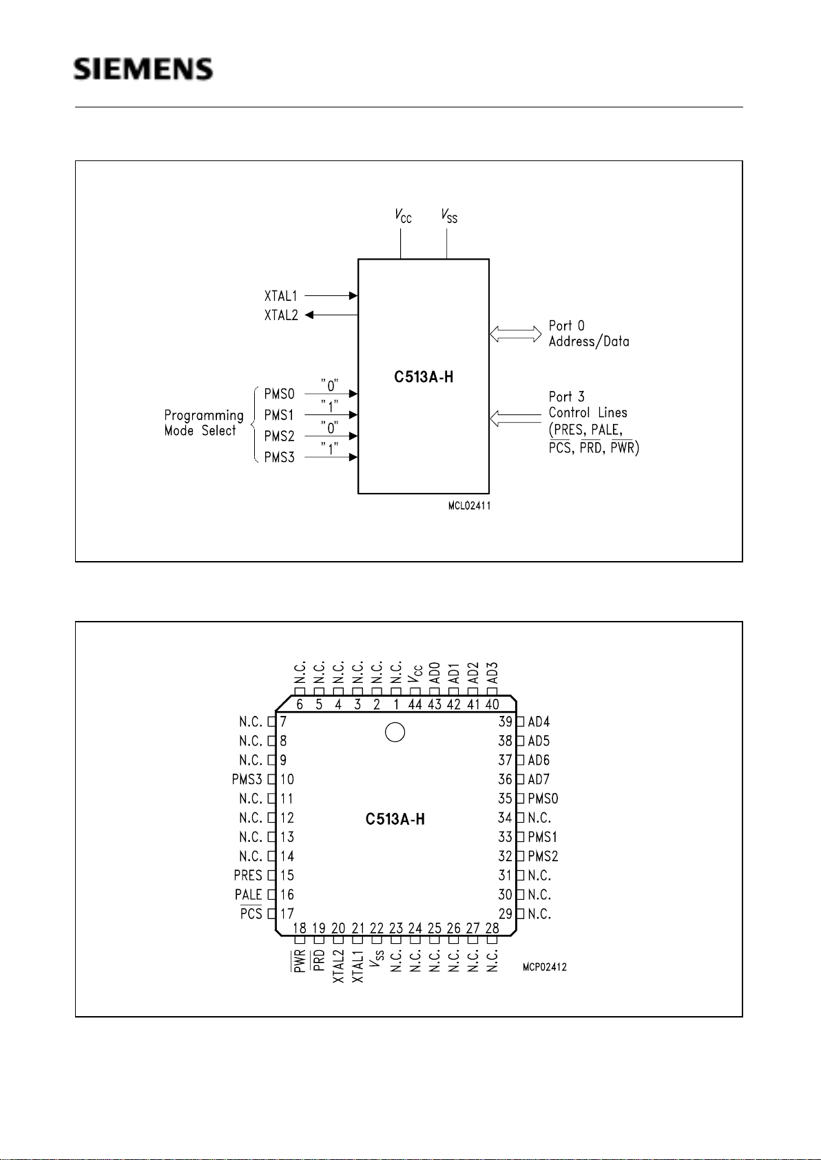
Figure 4
C513A-H Logic Symbol in Programming Mode
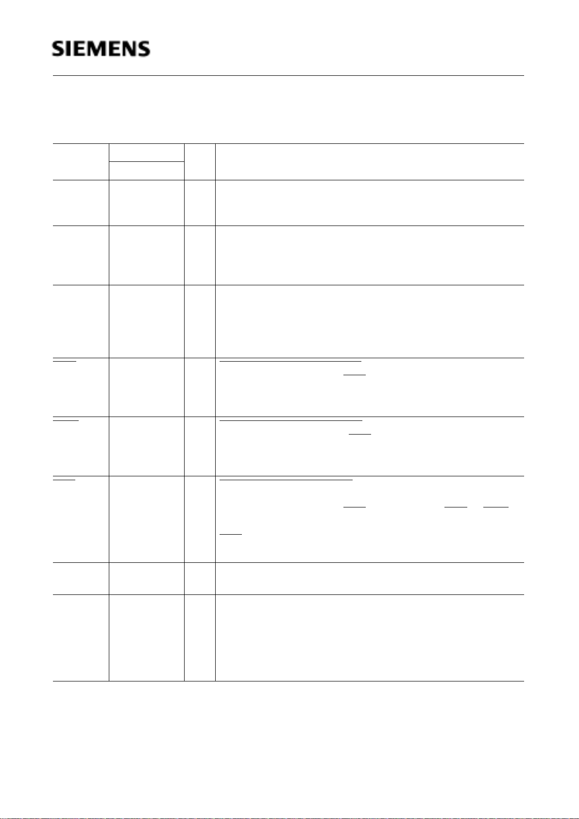
Figure 5
C513A-H Pin Configuration in Programming Mode (P-LCC-44)
C511 / C513
Semiconductor Group 13
Table 4
Pin Definitions and Functions in Programming Mode (C513A-H only)
Symbol Pin Number I/O*) Function
P-LCC-44
PRES 15 I Programming Interface Reset
A high level on this input resets the programming interface and
its registers to their initial state.
AD0 - AD7 43 - 36 I/O Bidirectional Address/Data Bus
AD0-7 is used to transfer data to and from the registers of the
programming interface and to read the data of the memory field
during EEPROM verification.
PALE 16 I Programming Address Latch Enable
This input is used to latch address information at AD0-7. The
trailing edge of PALE is used to latch the register addresses.
Each read or write access in programming mode must be
initiated by a PALE high pulse.
PRD
18 I Programming Read Control
A low level at this pin (and PCS
=low) enables the AD0-7 buffers
for reading of the data or control registers of the programming
interface.
PWR
19 I Programming Write Control
A low level at this pin (and PCS
=low) causes the data at AD07 to be written into the data or control registers of the
programming interface.
PCS
17 I Programming Chip Select
A low level at this pin enables the access to the registers of the
programming interface. If PCS
is active, either PRD or PWR
control whether data is read or written into the registers.
PCS
should be always deactivated between subsequent
accesses to the programming interface.
XTAL2 20 – XTAL2
Output of the inverting oscillator amplifier.
XTAL1 21 – XTAL1
Input to the inverting oscillator amplifier and input to the internal
clock generator circuits.
To drive the device from an external clock source, XTAL1
should be driven, while XTAL2 is left unconnected.
During the
device programming a clock must be always supplied.
*) I = Input
O = Output
 Loading...