


PLL with I2C Bus for AM/FM Receivers |
SDA 4331X |
1 |
|
Overview |
|
1.1 |
Features |
|
|
• 155 MHz FM and 40 MHz AM input frequency |
|
||
• 30 mVeff AM and 50 mVeff FM sensitivity |
|
||
• Additional open drain ports controlled by I2C Bus |
|
||
• 2-pin quartz oscillator |
|
||
• |
Fast phase detector with short anti-backlash pulses |
P-DSO-24-1 |
|
|
and polarity reversal |
|
|
•Charge pump current programmable in four steps up to 4.5 mA
•Frequency resolution of 1, 5 and 10 kHz AM and 12.5, 25 and 50 kHz FM
•P-DSO-24 package
Type |
Ordering Code |
Package |
|
|
|
SDA 4331X |
Q67100-H5139 |
P-DSO-24-1 |
|
|
|
1.2Application
The SDA 4331X provides separated input and output ports for AM and FM and is well suited for extremely fast loop settling times in the FM mode.
Semiconductor Group |
1 |
04.96 |
SDA 4331X
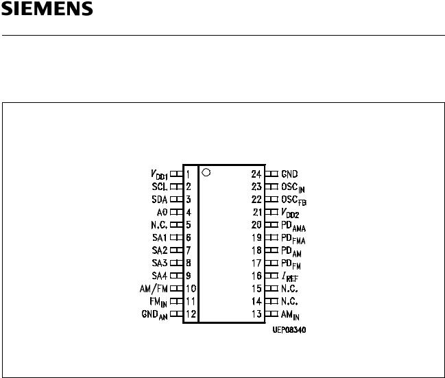
1.3Pin Configuration
(top view)
P-DSO-24-1
Figure 1
Semiconductor Group |
2 |
04.96 |

SDA 4331X
1.4Pin Definitions and Functions
Pin No. |
Symbol |
Input (I) |
Function |
|
|
Output (O) |
|
|
|
|
|
1 |
VDD1 |
|
Supply voltage digital (5 V) |
2 |
SCL |
I |
Clock I2C Bus |
|
|
|
|
3 |
SDA |
I/O |
Data I2C Bus |
|
|
|
|
4 |
A0 |
I |
Address selection, sets the LSB of the IC-address |
|
|
|
|
5 |
N.C. |
|
|
|
|
|
|
6 … 9 |
SA1 … SA4 |
O |
10 V open drain output, controlled via I2C Bus |
|
|
|
|
10 |
AM/FM |
O |
10 V open drain output, indicating the operation |
|
|
|
mode (H = AM) |
|
|
|
|
11 |
FMIN |
I |
Input for the FM signal from VCO |
12 |
GNDAN |
|
Ground analog |
|
|
|
|
13 |
AMIN |
I |
Input for the AM signal from VCO |
|
|
|
|
14 |
N.C. |
|
|
|
|
|
|
15 |
N.C. |
|
|
|
|
|
|
16 |
IREF |
I |
Reference current, setting the base current level |
|
|
|
for the charge pumps |
|
|
|
|
17 |
PDFM |
O |
FM charge pump output |
|
|
|
|
18 |
PDAM |
O |
AM charge pump output |
|
|
|
|
19 |
PDFMA |
O |
Source follower output FM |
20 |
PDAMA |
O |
Source follower output AM |
21 |
VDD2 |
|
Supply voltage digital for charge pump and source |
|
|
|
followers (up to 10 V) |
|
|
|
|
22 |
OSCFB |
I/O |
Oscillator feedback, quartz terminal |
|
|
|
|
23 |
OSCIN |
I |
Oscillator input, quartz terminal, optionally input |
|
|
|
for external reference |
|
|
|
|
24 |
GND |
|
Ground digital |
|
|
|
|
Semiconductor Group |
3 |
04.96 |

SDA 4331X
1.5Functional Block Diagram
Figure 2
Block Diagram
Semiconductor Group |
4 |
04.96 |
 Loading...