


Siemens SAB80C517A-M18, SAB80C517A-N18, SAB80C517A-N18-T3, SAB83C517A-N18-T4, SAB83C517A-5N18 Datasheet
...Microcomputer Components
8-Bit CMOS Single-Chip Microcontroller
SAB 80C517A/83C517A-5
Data Sheet 05.94

High-Performance |
SAB 80C517A/83C517A-5 |
8-Bit CMOS Single-Chip Microcontroller |
|
Preliminary |
|
SAB 83C517A-5 |
Microcontroller with factory mask-programmable ROM |
SAB 80C517A |
Microcontroller for external ROM |
●SAB 80C517A/83C517A-5, up to 18 MHz operation
●32 K × 8 ROM (SAB 83C517A-5 only, ROM-Protection available)
●256 × 8 on-chip RAM
●2 K × 8 on-chip RAM (XRAM)
●Superset of SAB 80C51 architecture:
–1 µs instruction cycle time at 12 MHz
–666 ns instruction cycle time at 18 MHz
–256 directly addressable bits
–Boolean processor
–64 Kbyte external data and program memory addressing
●Four 16-bit timer/counters
●Powerful 16-bit compare/capture unit
(CCU) with up to 21 high-speed or PWM output channels and 5 capture inputs
●Versatile "fail-safe" provisions
●Fast 32-bit division, 16-bit multiplication,
32-bit normalize and shift by peripheral MUL/DIV unit (MDU)
●Eight data pointers for external memory addressing
●Seventeen interrupt vectors, four priority levels selectable
●Genuine 10-bit A/D converter with 12 multiplexed inputs
●Two full duplex serial interfaces with programmable Baudrate-Generators
●Fully upward compatible with SAB 80C515,
SAB 80C517, SAB 80C515A
●Extended power saving mode
●Fast Power-On Reset
●Nine ports: 56 I/O lines, 12 input lines
●Three temperature ranges available:
0 to 70 oC (T1)
–40 to 85oC (T3)
–40 to 110oC (T4)
●Plastic packages: P-LCC-84,
P-MQFP-100-2
The SAB 80C517A/83C517A-5 is a high-end member of the Siemens SAB 8051 family of microcontrollers. It is designed in Siemens ACMOS technology and based on SAB 8051 architecture. ACMOS is a technology which combines high-speed and density characteristics with low-power consumption or dissipation.
While maintaining all the SAB 80C517 features and operating characteristics the SAB 80C517A is expanded in its "fail-safe" characteristics and timer capabilities.The
SAB 80C517A is identical with the SAB 83C517A-5 except that it lacks the on-chip program memory. The SAB 80C517A/83C517A-5 is supplied in a 84-pin plastic leaded chip carrier package (P-LCC-84) and in a 100-pin plastic quad flat package (P-MQFP-100-2).
Semiconductor Group |
1 |
1994-05-01 |

SAB 80C517A/83C517A-5
SAB 80C517A/83C517A-5 |
|
|
|
|||
Revision History |
05.94 |
|
|
|||
|
|
|||||
Previous Releases |
01.94/08.93/11.92/10.91/04.91 |
|||||
|
|
|||||
Page |
Subjects (changes since last revision 04.91) |
|||||
|
|
|||||
6 |
– Pin configuration P-MQFP-100-2 added |
|||||
4 |
– Pin differences updated |
|||||
7-15 |
– Pin numbers for P-MQFP-100-2 package added |
|||||
several |
– Correction of P-MRFP-100 into P-MQFP-100-2 |
|||||
3 |
– Ordering information for -40 to +110°C versions |
|||||
26, 27, 31 |
– Correction of register names S0RELL, SCON, ADCON, ICRON, |
|||||
|
and SBUF |
|||||
34 |
– Figure 4 corrected |
|||||
41 |
– Figure 8 corrected |
|||||
49 |
– |
|
|
|
|
|
PE/SWD function description completed |
||||||
60 |
– Correct ordering numbers |
|||||
62 |
– Test condition for VOH, VOH1 corrected |
|||||
65 |
– tPXIZ name corrected |
|||||
|
tAVIV, tAZPL values corrected |
|||||
several |
– Minimum clock frequence is now 3.5 MHz |
|||||
66 |
– tQVWH (data setup before |
WR |
) corrected and added |
|||
66 |
– tLLAX2 corrected |
|||||
Page |
Subjects (changes since last revision 08.93) |
|||||
|
|
|||||
26 |
– Corrected SFR name S0RELL |
|||||
51 |
– Below "Termination of HWPD Mode": 4th paragraph with ident |
|||||
|
|
corrected |
|
|
|
|
65 |
– Description of tLLIV corrected |
|||||
65 |
– Program Memory Read Cycle: tPXAV added |
|||||
74 |
– Oscillator circuit drawings: MQFP-100-2 pin numbers added. |
|||||
|
|
|||||
Page |
Subjects (changes since last revision 01.94) |
|||||
|
|
|||||
|
– Minor changes on several pages |
|||||
47 |
– Table 6 corrected |
|||||
|
|
|
|
|
|
|
Semiconductor Group |
2 |
1994-05-01 |
SAB 80C517A/83C517A-5
Ordering Information
Type |
Ordering |
Package |
Description |
|
|
Code |
|
8-bit CMOS Microcontroller |
|
|
|
|
|
|
SAB 80C517A-N18 |
Q67120-C583 |
P-LCC-84 |
for external memory,18 MHz |
|
|
|
|
||
SAB 80C517A-M18 |
TBD |
P-MQFP-100-2 |
||
|
||||
|
|
|
|
|
SAB 83C517A-5N18 |
Q67120-C582 |
P-LCC-84 |
with mask-programmable ROM, |
|
|
|
|
18 MHz |
|
|
|
|
|
|
SAB 80C517A-N18-T3 |
Q67120-C769 |
P-LCC-84 |
for external memory,18 MHz |
|
|
|
|
ext. temperature – 40 to 85 oC |
|
|
|
|
|
|
SAB 83C517A-5N18- |
Q67120-C771 |
P-LCC-84 |
with mask-programmable ROM, |
|
T3 |
|
|
18 MHz |
|
|
|
|
ext. temperature – 40 to 85 oC |
|
|
|
|
|
|
SAB 83C517A-N18-T4 |
TBD |
P-LCC-84 |
for external memory, 18 MHz |
|
|
|
|
ext. temperature -40 to +110oC |
|
|
|
|
|
|
SAB 83C517A-5N18- |
TBD |
P-LCC-84 |
with mask-programmable ROM, |
|
T4 |
|
|
18 MHz |
|
|
|
|
ext. temperature -40 to +110oC |
|
|
|
|
|
Semiconductor Group |
3 |
1994-05-01 |
SAB 80C517A/83C517A-5
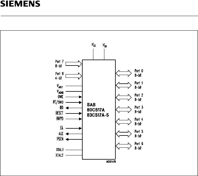
Logic Symbol
Semiconductor Group |
4 |
1994-05-01 |
SAB 80C517A/83C517A-5
The pin functions of the SAB 80C517A are identical with those of the SAB 80C517/80C537 with one exception:
Typ |
|
SAB 80C517A |
SAB 80C517/80C537 |
||||
|
|
|
|
|
|
|
|
P-LCC-84, Pin 60 |
|
|
|
|
|
|
|
|
|
|
HWPD |
|
|
N.C. |
|
P-MQFP-100-2, Pin 36 |
|
|
|
||||
|
|
|
|
|
|
||
|
|
|
|
|
|
|
|
|
|
|
|
|
|
|
|
|
|
|
|
|
|
|
|
|
|
|
|
|
|
|
|
|
|
|
|
|
|
|
|
|
|
|
|
|
|
|
|
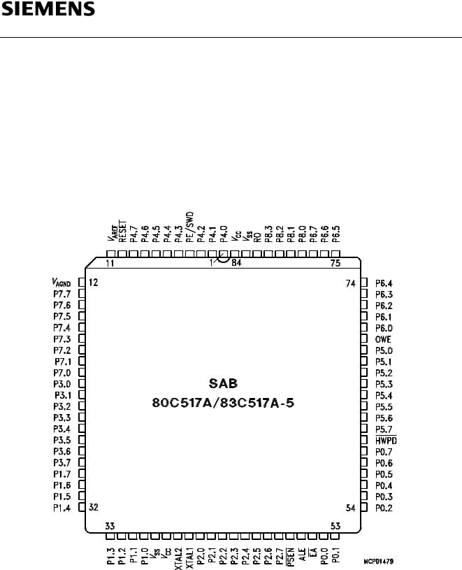
Pin Configuration
(P-LCC-84)
Semiconductor Group |
5 |
1994-05-01 |
|
|
SAB 80C517A/83C517A-5 |
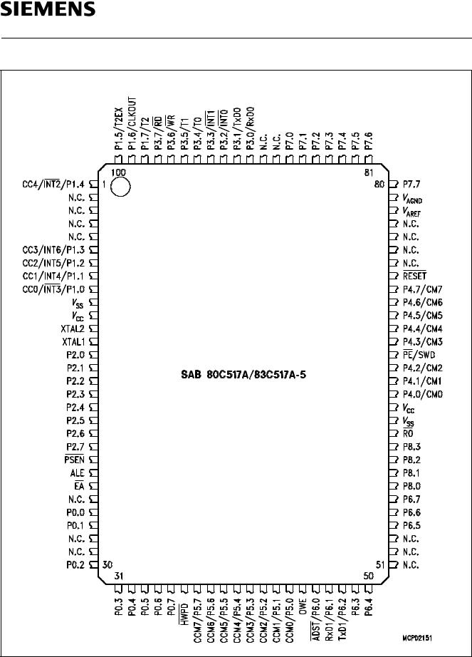
Pin Configuration |
|
|
(P-MQFP-100-2) |
|
|
Semiconductor Group |
6 |
1994-05-01 |

SAB 80C517A/83C517A-5
Pin Definitions and Functions
|
Symbol |
Pin Number |
I/O *) |
Function |
||||
|
|
|
|
|
|
|
|
|
|
|
|
P-LCC-84 |
P-MQFP-100-2 |
|
|
|
|
|
|
|
|
|
|
|||
|
P4.0 – P4.7 |
1– 3, 5 – 9 |
64 - 66, |
I/O |
Port 4 |
|||
|
|
|
|
68 - 72 |
|
is a bidirectional I/O port with internal |
||
|
|
|
|
|
|
pull-up resistors. Port 4 pins that have 1 |
||
|
|
|
|
|
|
s written to them are pulled high by the |
||
|
|
|
|
|
|
internal pull-up resistors, and in that |
||
|
|
|
|
|
|
state can be used as inputs. As inputs, |
||
|
|
|
|
|
|
port 4 pins being externally pulled low |
||
|
|
|
|
|
|
will source current (IIL, in the DC char- |
||
|
|
|
|
|
|
acteristics) because of the internal pull- |
||
|
|
|
|
|
|
up resistors. |
||
|
|
|
|
|
|
This port also serves alternate compare |
||
|
|
|
|
|
|
functions. The secondary functions are |
||
|
|
|
|
|
|
assigned to the pins of port 4 as follows: |
||
|
|
|
|
|
|
– CM0 (P4.0): Compare Channel 0 |
||
|
|
|
|
|
|
– CM1 (P4.1): Compare Channel 1 |
||
|
|
|
|
|
|
– CM2 (P4.2): Compare Channel 2 |
||
|
|
|
|
|
|
– CM3 (P4.3): Compare Channel 3 |
||
|
|
|
|
|
|
– CM4 (P4.4): Compare Channel 4 |
||
|
|
|
|
|
|
– CM5 (P4.5): Compare Channel 5 |
||
|
|
|
|
|
|
– CM6 (P4.6): Compare Channel 6 |
||
|
|
|
|
|
|
– CM7 (P4.7): Compare Channel 7 |
||
|
|
|
|
|
|
|
|
|
|
|
/SWD |
4 |
67 |
I |
Power saving modes |
|
Start |
PE |
enable |
|||||||
|
|
|
|
|
|
Watchdog Timer |
||
|
|
|
|
|
|
A low level on this pin allows the soft- |
||
|
|
|
|
|
|
ware to enter the power down, idle and |
||
|
|
|
|
|
|
slow down mode. In case the low level |
||
|
|
|
|
|
|
is also seen during reset, the watchdog |
||
|
|
|
|
|
|
timer function is off on default. |
||
|
|
|
|
|
|
Use of the software controlled power |
||
|
|
|
|
|
|
saving modes is blocked, when this pin |
||
|
|
|
|
|
|
is held on high level. A high level during |
||
|
|
|
|
|
|
reset performs an automatic start of the |
||
|
|
|
|
|
|
watchdog timer immediately after reset. |
||
|
|
|
|
|
|
When left unconnected this pin is pulled |
||
|
|
|
|
|
|
high by a weak internal pull-up resistor. |
||
|
|
|
|
|
|
|
|
|
*I = Input O = Output
Semiconductor Group |
7 |
1994-05-01 |

SAB 80C517A/83C517A-5
Pin Definitions and Functions (cont’d)
|
Symbol |
Pin Number |
I/O *) |
|
Function |
|||
|
|
|
P-LCC-84 |
P-MQFP-100-2 |
|
|
|
|
|
|
|
|
|
|
|
|
|
|
|
|
10 |
73 |
I |
|
|
|
RESET |
RESET |
|||||||
|
|
|
|
|
|
|
A low level on this pin for the duration of |
|
|
|
|
|
|
|
|
one machine cycle while the oscillator is |
|
|
|
|
|
|
|
|
running resets the SAB 80C517A. A |
|
|
|
|
|
|
|
|
small internal pull-up resistor permits |
|
|
|
|
|
|
|
|
power-on reset using only a capacitor |
|
|
|
|
|
|
|
|
connected to VSS. |
|
V AREF |
11 |
78 |
|
|
Reference voltage for the A/D con- |
|||
|
|
|
|
|
|
|
verter. |
|
|
|
|
|
|
|
|
||
|
V AGND |
12 |
79 |
|
|
Reference ground for the A/D |
||
|
|
|
|
|
|
|
converter. |
|
|
|
|
|
|
|
|
||
|
P7.7 -P7.0 |
13 - 20 |
80 - 87 |
I |
|
Port 7 |
||
|
|
|
|
|
|
|
is an 8-bit unidirectional input port. Port |
|
|
|
|
|
|
|
|
pins can be used for digital input, if |
|
|
|
|
|
|
|
|
voltage levels meet the specified input |
|
|
|
|
|
|
|
|
high/low voltages, and for the lower 8- |
|
|
|
|
|
|
|
|
bit of the multiplexed analog inputs of |
|
|
|
|
|
|
|
|
the A/D converter, simultaneously. |
|
|
|
|
|
|
|
|
|
|
* I = Input |
|
|
|
|
|
|
||
|
O = Output |
|
|
|
|
|
|
|
Semiconductor Group |
8 |
1994-05-01 |

SAB 80C517A/83C517A-5
Pin Definitions and Functions (cont’d)
Symbol |
|
Pin Number |
I/O *) |
Function |
|
|
|
|||||||
|
P-LCC-84 |
P-MQFP-100-2 |
|
|
|
|
|
|
|
|
|
|
|
|
|
|
|
|
|
|
|
|
|
||||||
P3.0 - P3.7 |
21 - 28 |
|
90 - 97 |
I/O |
Port 3 |
|
|
|
||||||
|
|
|
|
|
is a bidirectional I/O port with internal pull- |
|||||||||
|
|
|
|
|
up resistors. Port 3 pins that have 1 s |
|||||||||
|
|
|
|
|
written to them are pulled high by the |
|||||||||
|
|
|
|
|
internal pull-up resistors, and in that state |
|||||||||
|
|
|
|
|
can be used as inputs. As inputs, port 3 |
|||||||||
|
|
|
|
|
pins being externally pulled low will source |
|||||||||
|
|
|
|
|
current (IIL, in the DC characteristics) |
|||||||||
|
|
|
|
|
because of the internal pull-up resistors. |
|||||||||
|
|
|
|
|
Port 3 also contains the interrupt, timer, |
|||||||||
|
|
|
|
|
serial port 0 and external memory strobe |
|||||||||
|
|
|
|
|
pins that are used by various options. The |
|||||||||
|
|
|
|
|
output latch corresponding to a secondary |
|||||||||
|
|
|
|
|
function must be programmed to a one (1) |
|||||||||
|
|
|
|
|
for that function to operate. |
|||||||||
|
|
|
|
|
The secondary functions are assigned to |
|||||||||
|
|
|
|
|
the pins of port 3, as follows: |
|||||||||
|
|
|
|
|
– R × D0 (P3.0): receiver data input |
|||||||||
|
|
|
|
|
|
(asynchronous) or data input/output |
||||||||
|
|
|
|
|
|
(synchronous) of serial interface |
||||||||
|
|
|
|
|
– |
T × D0 (P3.1): transmitter data output |
||||||||
|
|
|
|
|
|
(asynchronous) or clock output |
||||||||
|
|
|
|
|
|
(synchronous) of serial interface 0 |
||||||||
|
|
|
|
|
– |
|
|
|
(P3.2): |
|
|
|
||
|
|
|
|
|
INT0 |
interrupt 0 input/timer 0 |
||||||||
|
|
|
|
|
|
gate control |
|
|
|
|||||
|
|
|
|
|
– |
|
|
|
(P3.3): |
|
|
|
|
|
|
|
|
|
|
INT1 |
|
interrupt 1 input/timer 1 |
|||||||
|
|
|
|
|
|
gate control |
|
|
|
|||||
|
|
|
|
|
– |
T0 (P3.4): |
counter 0 input |
|||||||
|
|
|
|
|
– |
T1 (P3.5): |
counter 1 input |
|||||||
|
|
|
|
|
– |
|
|
(P3.6): |
the write control signal |
|||||
|
|
|
|
|
WR |
|||||||||
|
|
|
|
|
|
latches the data byte from port 0 into the |
||||||||
|
|
|
|
|
|
external data memory |
||||||||
|
|
|
|
|
– |
|
(P3.7): |
the read control signal |
||||||
|
|
|
|
|
RD |
|||||||||
|
|
|
|
|
|
enables the external data memory to |
||||||||
|
|
|
|
|
|
port 0 |
|
|
|
|||||
|
|
|
|
|
|
|
|
|
|
|
|
|
|
|
*I = Input O = Output
Semiconductor Group |
9 |
1994-05-01 |
SAB 80C517A/83C517A-5
Pin Definitions and Functions (cont’d)
Symbol |
|
Pin Number |
I/O *) |
Function |
|
|
|
|
||||
|
P-LCC-84 |
P-MQFP-100-2 |
|
|
|
|
|
|
|
|
|
|
|
|
|
|
|
|
|
|
|
|
|||
P1.7 - P1.0 |
29 - 36 |
|
98 - 100, |
I/O |
Port 1 |
|
|
|
|
|||
|
|
|
1, 6 - 9 |
|
is a bidirectional I/O port with internal |
|||||||
|
|
|
|
|
pull-up resistors. Port 1 pins that have |
|||||||
|
|
|
|
|
1 s written to them are pulled high by the |
|||||||
|
|
|
|
|
internal pull-up resistors, and in that state |
|||||||
|
|
|
|
|
can be used as inputs. As inputs, port 1 |
|||||||
|
|
|
|
|
pins being externally pulled low will source |
|||||||
|
|
|
|
|
current (IIL, in the DC characteristics) |
|||||||
|
|
|
|
|
because of the internal pull-up resistors. It |
|||||||
|
|
|
|
|
is used for the low order address byte |
|||||||
|
|
|
|
|
during program verification. It also contains |
|||||||
|
|
|
|
|
the interrupt, timer, clock, capture and |
|||||||
|
|
|
|
|
compare pins that are used by various |
|||||||
|
|
|
|
|
options. The output latch must be |
|||||||
|
|
|
|
|
programmed to a one (1) for that function to |
|||||||
|
|
|
|
|
operate (except when used for the compare |
|||||||
|
|
|
|
|
functions). |
|
|
|
|
|||
|
|
|
|
|
The secondary functions are assigned to |
|||||||
|
|
|
|
|
the port 1 pins as follows: |
|||||||
|
|
|
|
|
– |
|
|
/CC0 (P1.0): |
|
|
|
|
|
|
|
|
|
INT3 |
interrupt 3 input/ |
||||||
|
|
|
|
|
|
compare 0 output /capture 0 input |
||||||
|
|
|
|
|
– |
INT4/CC1 (P1.1): |
interrupt 4 input / |
|||||
|
|
|
|
|
|
compare 1 output /capture 1 input |
||||||
|
|
|
|
|
– |
INT5/CC2 (P1.2): |
interrupt 5 input / |
|||||
|
|
|
|
|
|
compare 2 output /capture 2 input |
||||||
|
|
|
|
|
– |
INT6/CC3 (P1.3): |
interrupt 6 input / |
|||||
|
|
|
|
|
|
compare 3 output /capture 3 input |
||||||
|
|
|
|
|
– |
|
|
|
|
/ |
||
|
|
|
|
|
INT2/CC4 (P1.4): |
interrupt 2 input |
||||||
|
|
|
|
|
|
compare 4 output /capture 4 input |
||||||
|
|
|
|
|
– |
T2EX (P1.5): |
timer 2 external |
|||||
|
|
|
|
|
|
reload trigger input |
|
|
|
|
||
|
|
|
|
|
– |
CLKOUT (P1.6): |
system clock output |
|||||
|
|
|
|
|
– |
T2 (P1.7): |
counter 2 input |
|||||
|
|
|
|
|
|
|
|
|
|
|
|
|
*I = Input O = Output
Semiconductor Group |
10 |
1994-05-01 |

SAB 80C517A/83C517A-5
Pin Definitions and Functions (cont’d)
Symbol |
|
Pin Number |
I/O *) |
Function |
|
|
P-LCC-84 |
P-MQFP-100-2 |
|
|
|
|
|
|
|
|
|
XTAL2 |
39 |
|
12 |
– |
XTAL2 |
|
|
|
|
|
Input to the inverting oscillator amplifier and |
|
|
|
|
|
input to the internal clock generator circuits. |
|
|
|
|
|
|
XTAL1 |
40 |
|
13 |
– |
XTAL1 |
|
|
|
|
|
Output of the inverting oscillator amplifier. |
|
|
|
|
|
To drive the device from an external clock |
|
|
|
|
|
source, XTAL2 should be driven, while |
|
|
|
|
|
XTAL1 is left unconnected. There are no |
|
|
|
|
|
requirements on the duty cycle of the |
|
|
|
|
|
external clock signal, since the input to the |
|
|
|
|
|
internal clocking circuitry is devided down |
|
|
|
|
|
by a divide-by-two flip-flop. Minimum and |
|
|
|
|
|
maximum high and low times as well as |
|
|
|
|
|
rise/fall times specified in the AC |
|
|
|
|
|
characteristics must be observed. |
|
|
|
|
|
|
P2.0 - P2.7 |
41 - 48 |
|
14 - 21 |
I/O |
Port 2 |
|
|
|
|
|
is a bidirectional I/O port with internal pull- |
|
|
|
|
|
up resistors. Port 2 pins that have 1 s |
|
|
|
|
|
written to them are pulled high by the |
|
|
|
|
|
internal pull-up resistors, and in that state |
|
|
|
|
|
can be used as in-puts. As inputs, port 2 |
|
|
|
|
|
pins being externally pulled low will source |
|
|
|
|
|
current (IIL, in the DC characteristics) |
|
|
|
|
|
because of the internal pull-up resistors. |
|
|
|
|
|
Port 2 emits the high-order address byte |
|
|
|
|
|
during fetches from external program |
|
|
|
|
|
memory and during accesses to external |
|
|
|
|
|
data memory that use 16-bit addresses |
|
|
|
|
|
(MOVX @DPTR). In this application it uses |
|
|
|
|
|
strong internal pull-up resistors when |
|
|
|
|
|
issuing1 s. During accesses to external |
|
|
|
|
|
data memory that use 8-bit addresses |
|
|
|
|
|
(MOVX @Ri), port 2 issues the contents of |
|
|
|
|
|
the P2 special function register. |
|
|
|
|
|
|
*I = Input O = Output
Semiconductor Group |
11 |
1994-05-01 |

SAB 80C517A/83C517A-5
Pin Definitions and Functions (cont’d)
|
|
|
|
|
|
|
|
|
|
|
|
|
Symbol |
|
Pin Number |
I/O *) |
|
Function |
|||||||
|
|
|
|
P-LCC-84 |
P-MQFP-100-2 |
|
|
|
|
|
|
|
|
|
|
|
|
|
|
|
|
|
|
|
|
|
|
|
|
49 |
|
22 |
O |
|
The |
|
|
|
PSEN |
Program Store Enable |
|||||||||||
|
|
|
|
|
|
|
|
|
output is a control signal that enables the |
|||
|
|
|
|
|
|
|
|
|
external program memory to the bus during |
|||
|
|
|
|
|
|
|
|
|
external fetch operations. It is activated |
|||
|
|
|
|
|
|
|
|
|
every six oscillator periodes except during |
|||
|
|
|
|
|
|
|
|
|
external data memory accesses. Remains |
|||
|
|
|
|
|
|
|
|
|
high during internal program execution. |
|||
|
|
|
|
|
|
|
|
|||||
|
ALE |
50 |
|
23 |
O |
|
The Address Latch Enable |
|||||
|
|
|
|
|
|
|
|
|
output is used for latching the address into |
|||
|
|
|
|
|
|
|
|
|
external memory during normal operation. |
|||
|
|
|
|
|
|
|
|
|
It is activated every six oscillator periodes |
|||
|
|
|
|
|
|
|
|
|
except during an external data memory |
|||
|
|
|
|
|
|
|
|
|
access |
|||
|
|
|
|
|
|
|
|
|
|
|||
|
|
|
51 |
|
24 |
I |
|
|
|
|
||
|
EA |
External Access Enable |
||||||||||
|
|
|
|
|
|
|
|
|
When held at high level, instructions are |
|||
|
|
|
|
|
|
|
|
|
fetched from the internal ROM (SAB |
|||
|
|
|
|
|
|
|
|
|
83C517A-5 only) when the PC is less than |
|||
|
|
|
|
|
|
|
|
|
8000H. When held at low level, the SAB |
|||
|
|
|
|
|
|
|
|
|
80C517A fetches all instructions from ex- |
|||
|
|
|
|
|
|
|
|
|
ternal program memory. For the SAB |
|||
|
|
|
|
|
|
|
|
|
80C517A this pin must be tied low |
|||
|
|
|
|
|
|
|
|
|||||
|
P0.0 - P0.7 |
52 - 59 |
|
26 - 27, |
I/O |
|
Port 0 |
|||||
|
|
|
|
|
|
30 - 35 |
|
|
is an 8-bit open-drain bidirectional I/O port. |
|||
|
|
|
|
|
|
|
|
|
Port 0 pins that have 1 s written to them |
|||
|
|
|
|
|
|
|
|
|
float, and in that state can be used as high- |
|||
|
|
|
|
|
|
|
|
|
impe-dance inputs. Port 0 is also the |
|||
|
|
|
|
|
|
|
|
|
multiplexed low-order address and data |
|||
|
|
|
|
|
|
|
|
|
bus during accesses to external program or |
|||
|
|
|
|
|
|
|
|
|
data memory. In this application it uses |
|||
|
|
|
|
|
|
|
|
|
strong internal pull-up resistors when |
|||
|
|
|
|
|
|
|
|
|
issuing 1 s. Port 0 also out-puts the code |
|||
|
|
|
|
|
|
|
|
|
bytes during program verification in the |
|||
|
|
|
|
|
|
|
|
|
SAB 83C517A if ROM-Protection was not |
|||
|
|
|
|
|
|
|
|
|
enabled. External pull-up resistors are |
|||
|
|
|
|
|
|
|
|
|
required during program verification. |
|||
|
|
|
|
|
|
|
|
|
|
|
|
|
*I = Input O = Output
Semiconductor Group |
12 |
1994-05-01 |

SAB 80C517A/83C517A-5
Pin Definitions and Functions (cont’d)
|
|
|
|
|
|
|
|
|
|
Symbol |
|
Pin Number |
I/O *) |
|
Function |
||||
|
|
|
P-LCC-84 |
P-MQFP-100-2 |
|
|
|
|
|
|
|
|
|
|
|
|
|
|
|
|
|
|
60 |
|
36 |
I |
|
|
|
HWPD |
Hardware Power Down |
||||||||
|
|
|
|
|
|
|
|
A low level on this pin for the duration of |
|
|
|
|
|
|
|
|
|
one machine cycle while the oscillator is |
|
|
|
|
|
|
|
|
|
running resets the SAB 80C517A. A low |
|
|
|
|
|
|
|
|
|
level for a longer period will force the part to |
|
|
|
|
|
|
|
|
|
Power Down Mode with the pins floating. |
|
|
|
|
|
|
|
|
|
(see table 7) |
|
|
|
|
|
|
|
|
|
||
|
P5.7 - P5.0 |
61 - 68 |
|
37 - 44 |
I/O |
|
Port 5 |
||
|
|
|
|
|
|
|
|
is a bidirectional I/O port with internal pull- |
|
|
|
|
|
|
|
|
|
up resistors. Port 5 pins that have 1 s |
|
|
|
|
|
|
|
|
|
written to them are pulled high by the |
|
|
|
|
|
|
|
|
|
internal pull-up resistors, and in that state |
|
|
|
|
|
|
|
|
|
can be used as inputs. As inputs, port 5 |
|
|
|
|
|
|
|
|
|
pins being externally pulled low will source |
|
|
|
|
|
|
|
|
|
current (IIL, in the DC characteristics) |
|
|
|
|
|
|
|
|
|
because of the internal pull-up resistors. |
|
|
|
|
|
|
|
|
|
This port also serves the alternate function |
|
|
|
|
|
|
|
|
|
"Concurrent Compare" and "Set/Reset |
|
|
|
|
|
|
|
|
|
Compare". The secondary functions are |
|
|
|
|
|
|
|
|
|
assigned to the port 5 pins as follows: |
|
|
|
|
|
|
|
I |
|
– CCM0 to CCM7 (P5.0 to P5.7): |
|
|
|
|
|
|
|
|
concurrent compare or Set/Reset |
||
|
|
|
|
|
|
|
|
||
|
|
|
|
|
|
|
|
||
|
OWE |
69 |
|
45 |
I/O |
|
Oscillator Watchdog Enable |
||
|
|
|
|
|
|
|
|
A high level on this pin enables the |
|
|
|
|
|
|
|
|
|
oscillator watchdog. When left |
|
|
|
|
|
|
|
|
|
unconnected this pin is pulled high by a |
|
|
|
|
|
|
|
|
|
weak internal pull-up resistor. When held at |
|
|
|
|
|
|
|
|
|
low level the oscillator watchdog function is |
|
|
|
|
|
|
|
|
|
off. |
|
|
|
|
|
|
|
|
|
|
|
*I = Input O = Output
Semiconductor Group |
13 |
1994-05-01 |

SAB 80C517A/83C517A-5
Pin Definitions and Functions (cont’d)
Symbol |
|
Pin Number |
I/O *) |
Function |
|||
|
P-LCC-84 |
P-MQFP-100-2 |
|
|
|
|
|
|
|
|
|
|
|
||
P6.0 - P6.7 |
70 - 77 |
|
46 - 50, |
I/O |
Port 6 |
||
|
|
|
54 - 56 |
|
is a bidirectional I/O port with internal pull- |
||
|
|
|
|
|
up resistors. Port 6 pins that have 1 s |
||
|
|
|
|
|
written to them are pulled high by the |
||
|
|
|
|
|
internal pull-up resistors, and in that state |
||
|
|
|
|
|
can be used as inputs. As inputs, port 6 |
||
|
|
|
|
|
pins being externally pulled low will source |
||
|
|
|
|
|
current (I IL, in the DC characteristics) |
||
|
|
|
|
|
because of the internal pull-up resistors. |
||
|
|
|
|
|
Port 6 also contains the external A/D |
||
|
|
|
|
|
converter control pin and the transmit and |
||
|
|
|
|
|
receive pins for serial channel 1. The |
||
|
|
|
|
|
output latch corresponding to a secondary |
||
|
|
|
|
|
function must be programmed to a one (1) |
||
|
|
|
|
|
for that function to operate. |
||
|
|
|
|
|
The secondary functions are assigned to |
||
|
|
|
|
|
the pins of port 6, as follows: |
||
|
|
|
|
|
– |
|
(P6.0): external A/D converter |
|
|
|
|
|
ADST |
||
|
|
|
|
|
|
start pin |
|
|
|
|
|
|
– |
R × D1 (P6.1): receiver data input |
|
|
|
|
|
|
|
of serial interface 1 |
|
|
|
|
|
|
– |
T × D1 (P6.2): transmitter data output |
|
|
|
|
|
|
|
of serial interface 1 |
|
|
|
|
|
|
|
||
P8.0 - P8.3 |
78 - 81 |
|
57 - 60 |
I |
Port 8 |
||
|
|
|
|
|
is a 4-bit unidirectional input port. Port pins |
||
|
|
|
|
|
can be used for digital input, if voltage |
||
|
|
|
|
|
levels meet the specified input high/low |
||
|
|
|
|
|
voltages, and for the higher 4-bit of the |
||
|
|
|
|
|
multiplexed analog inputs of the A/D |
||
|
|
|
|
|
converter, simultaneously |
||
|
|
|
|
|
|
|
|
*I = Input O = Output
Semiconductor Group |
14 |
1994-05-01 |

SAB 80C517A/83C517A-5
Pin Definitions and Functions (cont’d)
Symbol |
Pin Number |
I/O *) |
Function |
|||||
|
|
P-LCC-84 |
P-MQFP-100-2 |
|
|
|
|
|
|
|
|
|
|
|
|
|
|
|
|
82 |
61 |
|
O |
|
|
|
RO |
|
Reset Output |
||||||
|
|
|
|
|
|
This pin outputs the internally |
||
|
|
|
|
|
|
synchronized reset request signal. This |
||
|
|
|
|
|
|
signal may be generated by an external |
||
|
|
|
|
|
|
hardware reset, a watchdog timer reset |
||
|
|
|
|
|
|
or an oscillator watch-dog reset. The |
||
|
|
|
|
|
|
reset output is active low. |
||
|
|
|
|
|
||||
VS S |
37, 83 |
10, 62 |
– |
Circuit ground potential |
||||
VCC |
38, 84 |
11, 63 |
– |
Supply Terminal for all operating |
||||
|
|
|
|
|
|
modes |
||
|
|
|
|
|
|
|||
N.C. |
– |
2 - 5, 25, |
– |
|
Not connected |
|||
|
|
|
28 |
- 29, |
|
|
|
|
|
|
|
51 |
- 53, |
|
|
|
|
|
|
|
74 |
- 77, |
|
|
|
|
|
|
|
88 |
- 89 |
|
|
|
|
|
|
|
|
|
|
|
|
|
*I = Input O = Output
Semiconductor Group |
15 |
1994-05-01 |

SAB 80C517A/83C517A-5
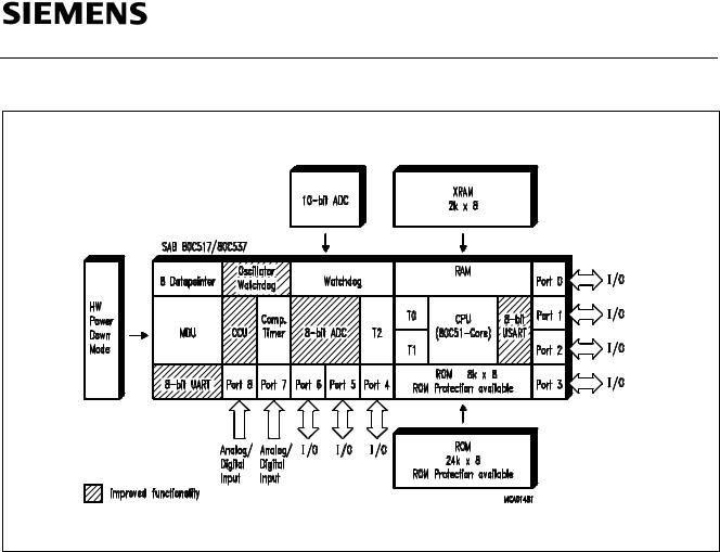
Figure 1
Block Diagram
Semiconductor Group |
16 |
1994-05-01 |
SAB 80C517A/83C517A-5
Functional Description
The SAB 80C517A is based on 8051 architecture. It is a fully compatible member of the
Siemens SAB 8051/80C51 microcontroller family being an significantly enhanced
SAB 80C517. The SAB 80C517A is therefore compatible with code written for the
SAB 80C517.
Having an 8-bit CPU with extensive facilities for bit-handling and binary BCD arithmetics the
SAB 80C517A is optimized for control applications. With a 18 MHz crystal, 58 % of the instructions are executed in 666.67 ns.
Being designed to close the performance gap to the 16-bit microcontroller world, the
SAB 80C517A’s CPU is supported by a powerful 32-/16-bit arithmetic unit and a more flexible addressing of external memory by eight 16-bit datapointers.
Memory Organisation
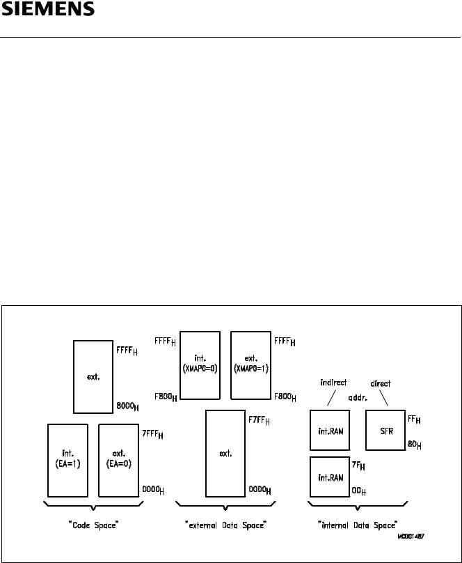
According to the SAB 8051 architecture, the SAB 80C517A has separate address spaces for program and data memory. Figure 2 illustrates the mapping of address spaces.
Figure 2
Memory Map
Semiconductor Group |
17 |
1994-05-01 |

SAB 80C517A/83C517A-5
Program Memory ('Code Space')
The SAB 83C517A-5 has 32 Kbyte of on-chip ROM, while the SAB 80C517A has no internal
ROM. The program memory can externally be expanded up to 64 Kbyte. Pin EA controls whether program fetches below address 8000H are done from internal or external memory.
As a new feature the SAB 83C517A-5 offers the possibility of protecting the internal ROM against unauthorized access. This protection is implemented in the ROM-Mask.Therefore, the decision ROM-Protection 'yes' or 'no' has to be made when delivering the ROM-Code. Once enabled, there is no way of disabling the ROM-Protection.
Effect: |
The access to internal ROM done by an externally fetched MOVC instruction |
|
is disabled. Nevertheless, an access from internal ROM to external ROM is possible. |
To verify the read protected ROM-Code a special ROM-Verify-Mode is implemented. This mode also can be used to verify unprotected internal ROM.
ROM -Protection |
ROM-Verification Mode |
Restrictions |
|
|
(see 'AC Characteristics') |
|
|
|
|
|
|
no |
ROM-Verification Mode 1 |
– |
|
|
(standard 8051 Verification Mode) |
|
|
|
ROM-Verification Mode 2 |
|
|
|
|
|
|
yes |
ROM-Verification Mode 2 |
– |
standard 8051 |
|
|
|
Verification Mode is |
|
|
|
disabled |
|
|
– |
externally applied MOVC |
|
|
|
accessing internal ROM |
|
|
|
is disabled |
|
|
|
|
Semiconductor Group |
18 |
1994-05-01 |

SAB 80C517A/83C517A-5
Data Memory ('Code Space')
The data memory space consists of an internal and an external memory space. The
SAB 80C517A contains another 2 Kbyte on On-Chip RAM above the 256-bytes internal RAM of the base type SAB 80C517. This RAM is called XRAM in this document.
External Data Memory
Up to 64 Kbyte external data memory can be addressed by instructions that use 8-bit or 16-bit indirect addressing. For 8-bit addressing MOVX instructions in combination with registers R0 and R1 can be used. A 16-bit external memory addressing is supported by eight 16-bit datapointers. Registers XPAGE and SYSCON are controlling whether data fetches at addresses F800H to FFFFH are done from internal XRAM or from external data memory.
Internal Data Memory
The internal data memory is divided into four physically distinct blocks:
–the lower 128 bytes of RAM including four banks containing eight registers each
–the upper 128 byte of RAM
–the 128 byte special function register area.
–a 2 K × 8 area which is accessed like external RAM (MOVX-instructions), implemented on
chip at the address range from F800H to FFFFH. Special Function Register SYSCON controls whether data is read or written to XRAM or external RAM.
A mapping of the internal data memory is also shown in figure 2. The overlapping address spaces are accessed by different addressing modes (see User's Manual SAB 80C517). The stack can be located anywhere in the internal data memory.
Architecture for the XRAM
The contents of the XRAM is not affected by a reset or HW Power Down. After power-up the contents is undefined, while it remains unchanged during and after a reset or HW Power Down if the power supply is not turned off.
The additional On-Chip RAM is logically located in the "external data memory" range at the upper end of the 64 Kbyte address range (F800H-FFFFH). It is possible to enable and disable (only by reset) the XRAM. If it is disabled the device shows the same behaviour as the parts without XRAM, i.e. all MOVX accesses use the external bus to physically external data memory.
Semiconductor Group |
19 |
1994-05-01 |
SAB 80C517A/83C517A-5
Accesses to XRAM
Because the XRAM is used in the same way as external data memory the same instruction types must be used for accessing the XRAM.
Note: If a reset occurs during a write operation to XRAM, the effect on XRAM depends on the cycle which the reset is detected at (MOVX is a 2-cycle instruction):
Reset detection at cycle 1: The new value will not be written to XRAM. The old value is not affected.
Reset detection at cycle 2: The old value in XRAM is overwritten by the new value.
Accesses to XRAM using the DPTR
There are a Read and a Write instruction from and to XRAM which use one of the 16-bit DPTR for indirect addressing. The instructions are:
MOVX A, |
@DPTR (Read) |
MOVX |
@DPTR, A (Write) |
Normally the use of these instructions would use a physically external memory. However, in the SAB 80C517A the XRAM is accessed if it is enabled and if the DPTR points to the XRAM
address space (DPTR  F800H).
Accesses to XRAM using the Registers R0/R1
The 8051 architecture provides also instructions for accesses to external data memory range which use only an 8-bit address (indirect addressing with registers R0 or R1). The instructions are:
MOVX A, |
@Ri (Read) |
MOVX |
@Ri, A (Write) |
In application systems, either a real 8-bit bus (with 8-bit address) is used or Port 2 serves as page register which selects pages of 256-byte. However, the distinction, whether Port 2 is used as general purpose I/O or as "page address" is made by the external system design. From the device’s point of view it cannot be decided whether the Port 2 data is used externally as address or as I/O data!
Hence, a special page register is implemented into the SAB 80C517A to provide the possibility of accessing the XRAM also with the MOVX @Ri instructions, i.e. XPAGE serves the same function for the XRAM as Port 2 for external data memory.
Semiconductor Group |
20 |
1994-05-01 |

SAB 80C517A/83C517A-5
Special Function Register XPAGE
Addr. 91H |
|
|
|
|
|
|
|
|
XPAGE |
The reset value of XPAGE is 00H.
XPAGE can be set and read by software.
The register XPAGE provides the upper address byte for accesses to XRAM with MOVX @Ri instructions. If the address formed from XPAGE and Ri is less than the XRAM address range, then an external access is performed. For the SAB 80C517A the contents of XPAGE must be greater or equal than F8H in order to use the XRAM. Of course, the XRAM must be enabled if it shall be used with MOVX @Ri instructions.
Thus, the register XPAGE is used for addressing of the XRAM; additionally its contents are used for generating the internal XRAM select. If the contents of XPAGE is less than the XRAM address range then an external bus access is performed where the upper address byte is provided by P2 and not by XPAGE!
Therefore, the software has to distinguish two cases, if the MOVX @Ri instructions with paging shall be used:
a) Access to XRAM: |
The upper address byte must be written to XPAGE |
|
or P2; both writes selects the XRAM address range. |
b) Access to external memory: The upper address byte must be written to P2; XPAGE will be loaded with the same address in order to deselect the XRAM.
Semiconductor Group |
21 |
1994-05-01 |

SAB 80C517A/83C517A-5
Control of XRAM in the SAB 80C517A
There are two control bits in register SYSCON which control the use and the bus operation during accesses to the additional On-Chip RAM (XRAM).
Special Function Register SYSCON
Addr. 0B1H |
— |
|
— |
— |
|
|
— |
|
— |
|
— |
|
XMAP1 |
XMAP0 |
SYSCON |
||||||||
|
|
|
|
|
|
|
|
|
|
|
|
|
|
|
|
|
|
|
|
|
|
|
|
Bit |
|
Function |
|
|
|
|
|
|
|
|
|
|
|
|
|
|
|
|
|
|
|
|
|
|
|
|
|
|
|
||||||||||||||||||
XMAP0 |
|
Global enable/disable bit for XRAM memory. |
|||||||||||||||||||||
|
|
XMAP0 = 0: The |
|
access |
|
to XRAM |
(= On-Chip XDATA memory) is en- |
||||||||||||||||
|
|
abled. |
|
|
|
|
|
|
|
|
|
|
|
|
|
|
|
|
|
|
|
|
|
|
|
XMAP0 = 1: The access to XRAM is disabled. All MOVX accesses are per- |
|||||||||||||||||||||
|
|
formed by the external bus (reset state). |
|
|
|
|
|||||||||||||||||
|
|
|
|
|
|
|
|
|
|
|
|
|
|
|
|
|
|
||||||
XMAP1 |
|
Control bit for |
|
|
|
|
|
|
|
|
|
|
|
|
|
|
|
|
|
|
|
||
|
RD/WR signals during accesses to XRAM; this bit has no |
||||||||||||||||||||||
|
|
effect if XRAM is disabled (XMAP0 = 1) or if addresses exceeding the |
|||||||||||||||||||||
|
|
XRAM address range are used for MOVX accesses. |
|||||||||||||||||||||
|
|
XMAP1 = 0: The signals |
|
|
|
and |
|
|
are not activated during accesses |
||||||||||||||
|
|
RD |
WR |
||||||||||||||||||||
|
|
to XRAM. |
|
|
|
|
|
|
|
|
|
|
|
|
|
|
|
|
|
|
|
|
|
|
|
XMAP1 = 1: The signals |
|
|
and |
|
|
are activated during accesses to |
|||||||||||||||
|
|
|
RD |
WR |
|||||||||||||||||||
|
|
XRAM. |
|
|
|
|
|
|
|
|
|
|
|
|
|
|
|
|
|
|
|
|
|
|
|
|
|
|
|
|
|
|
|
|
|
|
|
|
|
|
|
|
|
|
|
|
|
Reset value of SYSCON is xxxx xx01B.
The control bit XMAP0 is a global enable/disable bit for the additional On-Chip RAM (XRAM). If this bit is set, the XRAM is disabled, all MOVX accesses use external memory via the external bus. In this case the SAB 80C517A does not use the additional On-Chip RAM and is compatible with the types without XRAM.
Semiconductor Group |
22 |
1994-05-01 |
SAB 80C517A/83C517A-5
XMAP0 is hardware protected by an unsymmetric latch. An unintentional disabling of XRAM could be dangerous since indeterminate values would be read from external bus. To avoid this the XMAP-bit is forced to '1' only by reset. Additionally, during reset an internal capacitor is loaded. So after reset state XRAM is disabled. Because of the load time of the capacitor
XMAP0-bit once written to '0' (that is, discharging capacitor) cannot be set to '1' again by software. On the other hand any distortion (software hang up, noise, ...) is not able to load this capacitor, too. That is, the stable status is XRAM enabled. The only way to disable XRAM after it was enabled is a reset.
The clear instruction for XMAP0 should be integrated in the program initialization routine before XRAM is used. In extremely noisy systems the user may have redundant clear instructions.
The control bit XMAP1 is relevant only if the XRAM is accessed. In this case the externa RD and WR signals at P3.6 and P3.7 are not activated during the access, if XMAP1 is cleared. For debug purposes it might be useful to have these signals and the addresses at Ports 0.2 available. This is performed if XMAP1 is set.
The behaviour of Port 0 and P2 during a MOVX access depends on the control bits in register SYSCON and on the state of pin EA. The table 1 lists the various operating conditions. It shows the following characteristics:
a)Use of P0 and P2 pins during the MOVX access.
Bus: The pins work as external address/data bus. If (internal) XRAM is accessed, the data written to the XRAM can be seen on the bus in debug mode.
I/0: The pins work as Input/Output lines under control of their latch.
b)Activation of the RD and WR pin during the access.
c)Use of internal or external XDATA memory.
The shaded areas describe the standard operation as each 80C51 device without on-chip XRAM behaves.
Semiconductor Group |
23 |
1994-05-01 |
 Loading...