


Siemens SAB-C502-2R20N, SAB-C502-2R20P, SAB-C502-2RN, SAB-C502-2RP, SAB-C502-L20N Datasheet
...Microcomputer Components
8-Bit CMOS Microcontroller
C502
Data Sheet 08.94
|
.de/ |
|
.siemens |
|
Semiconductor/ |
ttp://www |
|
h |
|
8-Bit CMOS Microcontroller |
C502 |
Preliminary
●Fully compatible to standard 8051 microcontroller
●Versions for 12 / 20 MHz operating frequency
●16 K × 8 ROM (SAB-C502-2R only)
●256 × 8 RAM
●256 × 8 XRAM (additional on-chip RAM)
●Eight datapointers for indirect addressing of program and external data memory (including XRAM)
●Four 8-bit ports
●Three 16 -bit Timers / Counters (Timer 2 with Up/Down Counter feature)
●USART with programmable 10-bit Baudrate-Generator
●Six interrupt sources, two priority levels
●Programmable 15-bit Watchdog Timer
●Oscillator Watchdog
●Fast Power On Reset
●Power Saving Modes
●P-DIP-40 package and P-LCC-44 package
● Temperature ranges: SAB-C502 |
TA: 0 ˚C to 70 ˚C |
SAF-C502 |
TA: – 40 ˚C to 85 ˚C |
SAB-C502
Semiconductor Group |
1 |
08.94 |

C502
The SAB-C502-L/C502-2R described in this document is compatible with the SAB 80C52 and can be used for all present SAB 80C52 applications.
The SAB-C502-2R contains a non-volatile 16 K × 8 read-only program memory, a volatile 256 × 8 read/write data memory, four ports, three 16-bit timers/counters, a six source, two priority level interrupt structure, a serial port and versatile fail save mechanisms. The SAB-C502-L/C502-2R incorporates 256 × 8 additional on-chip RAM called XRAM. For higher performance eight datapointers are implemented. The SAB-C502-L is identical, except that it lacks the program memory on chip. Therefore the term SAB-C502 refers to both versions within this specification unless otherwise noted.
Semiconductor Group |
2 |

C502
Ordering Information
Type |
Ordering |
Package |
Description |
|
Code |
|
(8-Bit CMOS microcontroller) |
|
|
|
|
SAB-C502-LN |
Q67120-C838 |
P-LCC-44 |
for external memory 12 MHz |
SAB-C502-LP |
Q67120-C889 |
P-DIP-40 |
|
|
|
|
|
SAB-C502-2RN |
Q67120-C839 |
P-LCC-44 |
with mask-programmable ROM, |
SAB-C502-2RP |
Q67120-C890 |
P-DIP-40 |
12 MHz |
|
|
|
|
SAB-C502-L20N |
Q67120-C885 |
P-LCC-44 |
for external memory 20 MHz |
SAB-C502-L20P |
Q67120-C891 |
P-DIP-40 |
|
|
|
|
|
SAB-C502-2R20N |
Q67120-C884 |
P-LCC-44 |
with mask-programmable ROM, |
SAB-C502-2R20P |
Q67120-C892 |
P-DIP-40 |
20 MHz |
|
|
|
|
SAF-C502-LN |
Q67120-C883 |
P-LCC-44 |
for external ROM, 12 MHz, |
SAF-C502-LP |
Q67120-C893 |
P-DIP-40 |
ext. temp. – 40 ˚C to 85 ˚C |
|
|
|
|
SAF-C502-2RN |
Q67120-C886 |
P-LCC-44 |
with mask-programmable ROM, |
SAF-C502-2RP |
Q67120-C894 |
P-DIP-40 |
12 MHz, ext. temp. – 40 ˚C to 85 ˚C |
|
|
|
|
SAF-C502-L20N |
Q67120-C887 |
P-LCC-44 |
for external memory, 20 MHz, |
SAF-C502-L20P |
Q67120-C895 |
P-DIP-40 |
ext. temp. – 40 ˚C to 85 ˚C |
|
|
|
|
SAF-C502-2R20N |
Q67120-C888 |
P-LCC-44 |
with mask-programmable ROM, |
SAF-C502-2R20P |
Q67120-C896 |
P-DIP-40 |
20 MHz, ext. temp. – 40 ˚C to 85 ˚C |
|
|
|
|
Note: Extended temperature range – 40 ˚C to 110 ˚C (SAH-C502) on request.
Semiconductor Group |
3 |
C502
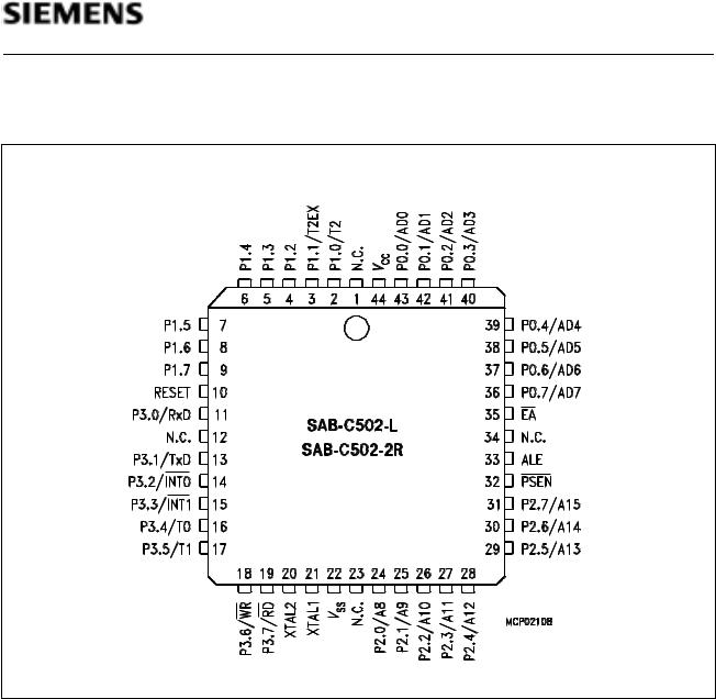
Pin Configuration
(top view)
(P-LCC-44)
Semiconductor Group |
4 |
C502
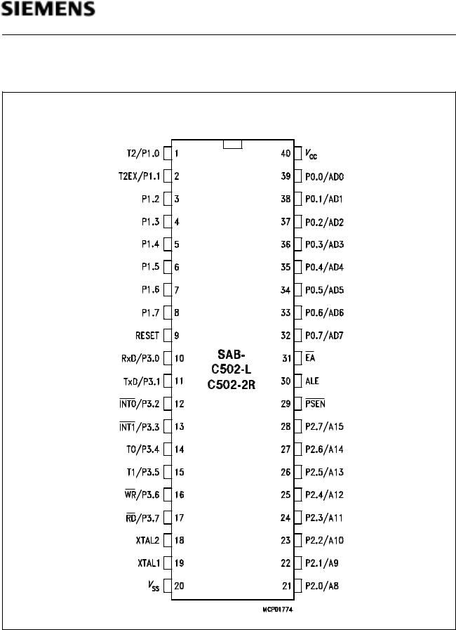
Pin Configuration
(top view)
(P-DIP-40)
Semiconductor Group |
5 |
C502
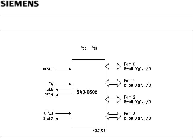
Logic Symbol
Semiconductor Group |
6 |

C502
Pin Definitions and Functions
Symbol |
|
Pin Number |
I/O*) |
Function |
|
||
|
|
|
|
|
|
||
|
P-LCC-44 |
P-DIP-40 |
|
|
|
|
|
|
|
|
|
|
|
|
|
P1.7 – P1.0 |
9–2 |
|
8–1 |
I |
Port 1 |
|
|
|
|
|
|
|
is a bidirectional I/O port with internal pull-up |
||
|
|
|
|
|
resistors. Port 1 pins that have 1s written to |
||
|
|
|
|
|
them are pulled high by the internal pull-up |
||
|
|
|
|
|
resistors, and in that state can be used as |
||
|
|
|
|
|
inputs. As inputs, port 1 pins being externally |
||
|
|
|
|
|
pulled low will source current (IIL, in the DC |
||
|
|
|
|
|
characteristics) because of the internal pull-up |
||
|
|
|
|
|
resistors. Port 1 also contains the timer 2 pins |
||
|
|
|
|
|
as secondary function. The output latch corre- |
||
|
|
|
|
|
sponding to a secondary function must be pro- |
||
|
|
|
|
|
grammed to a one (1) for that function to |
||
|
|
|
|
|
operate. |
|
|
|
|
|
|
|
The secondary functions are assigned to the |
||
|
|
|
|
|
pins of port 1, as follows: |
||
|
2 |
|
1 |
|
P1.0 |
T2 |
Input to counter 2 |
|
3 |
|
2 |
|
P1.1 |
T2EX |
Capture - Reload trigger of |
|
|
|
|
|
|
|
timer 2 / Up-Down count |
|
|
|
|
|
|
|
|
*) I = Input
O = Output
Semiconductor Group |
7 |

C502
Pin Definitions and Functions (cont’d)
Symbol |
|
Pin Number |
I/O*) |
Function |
|
|
|
|||||
|
|
|
|
|
|
|
|
|
|
|
||
|
P-LCC-44 |
P-DIP-40 |
|
|
|
|
|
|
|
|
|
|
|
|
|
|
|
|
|
|
|
|
|
|
|
P3.0 – P3.7 |
11, 13–19 |
10–17 |
I/O |
Port 3 |
|
|
|
|
|
|
|
|
|
|
|
|
|
is a bidirectional I/O port with internal pull-up |
|||||||
|
|
|
|
|
resistors. Port 3 pins that have 1s written to |
|||||||
|
|
|
|
|
them are pulled high by the internal pull-up |
|||||||
|
|
|
|
|
resistors, and in that state can be used as |
|||||||
|
|
|
|
|
inputs. As inputs, port 3 pins being externally |
|||||||
|
|
|
|
|
pulled low will source current (IIL, in the DC |
|||||||
|
|
|
|
|
characteristics) because of the internal pull-up |
|||||||
|
|
|
|
|
resistors. Port 3 also contains the interrupt, |
|||||||
|
|
|
|
|
timer, serial port 0 and external memory strobe |
|||||||
|
|
|
|
|
pins that are used by various options. The out- |
|||||||
|
|
|
|
|
put latch corresponding to a secondary func- |
|||||||
|
|
|
|
|
tion must be programmed to a one (1) for that |
|||||||
|
|
|
|
|
function to operate. |
|||||||
|
|
|
|
|
The secondary functions are assigned to the |
|||||||
|
|
|
|
|
pins of port 3, as follows: |
|||||||
|
11 |
|
10 |
|
P3.0 |
R×D |
receiver data input |
|||||
|
|
|
|
|
|
|
|
|
|
(asynchronous) or data input/ |
||
|
|
|
|
|
|
|
|
|
|
output (synchronous) of serial |
||
|
|
|
|
|
|
|
|
|
|
interface 0 |
||
|
13 |
|
11 |
|
P3.1 |
T×D |
transmitter data output |
|||||
|
|
|
|
|
|
|
|
|
|
(asynchronous) or clock output |
||
|
|
|
|
|
|
|
|
|
|
(synchronous) of the serial |
||
|
|
|
|
|
|
|
|
|
|
interface 0 |
||
|
14 |
|
12 |
|
P3.2 |
|
|
|
|
interrupt 0 |
|
|
|
|
INT0 |
input/timer 0 gate |
|||||||||
|
|
|
|
|
|
|
|
|
|
control |
||
|
15 |
|
13 |
|
P3.3 |
|
|
|
|
interrupt 1 |
|
|
|
|
INT1 |
input/timer 1 gate |
|||||||||
|
|
|
|
|
|
|
|
|
|
control |
||
|
16 |
|
14 |
|
P3.4 |
T0 |
counter 0 input |
|||||
|
17 |
|
15 |
|
P3.5 |
T1 |
counter 1 input |
|||||
|
18 |
|
16 |
|
P3.6 |
|
|
|
the write control signal latches |
|||
|
|
WR |
||||||||||
|
|
|
|
|
|
|
|
|
|
the data byte from port 0 into the |
||
|
|
|
|
|
|
|
|
|
|
external data memory |
||
|
19 |
|
17 |
|
P3.7 |
|
|
the read control signal enables |
||||
|
|
RD |
||||||||||
|
|
|
|
|
|
|
|
|
|
the external data memory to |
||
|
|
|
|
|
|
|
|
|
|
port 0 |
||
|
|
|
|
|
|
|
|
|
||||
XTAL2 |
20 |
|
18 |
– |
XTAL2 |
|
|
|
||||
|
|
|
|
|
Output of the inverting oscillator amplifier |
|||||||
|
|
|
|
|
|
|
|
|
|
|
|
|
*)I = Input O = Output
Semiconductor Group |
8 |

C502
Pin Definitions and Functions (cont’d)
Symbol |
Pin Number |
I/O*) |
Function |
||||
|
|
|
|
|
|
|
|
|
|
P-LCC-44 |
P-DIP-40 |
|
|
|
|
|
|
|
|
|
|||
XTAL1 |
21 |
19 |
– |
XTAL1 |
|||
|
|
|
|
|
Input to the inverting oscillator amplifier and |
||
|
|
|
|
|
input to the internal clock generator circuits. |
||
|
|
|
|
|
To drive the device from an external clock |
||
|
|
|
|
|
source, XTAL1 should be driven, while XTAL2 |
||
|
|
|
|
|
is left unconnected. There are no requirements |
||
|
|
|
|
|
on the duty cycle of the external clock signal, |
||
|
|
|
|
|
since the input to the internal clocking circuitry |
||
|
|
|
|
|
is divided down by a divide-by-two flip-flop. |
||
|
|
|
|
|
Minimum and maximum high and low times as |
||
|
|
|
|
|
well as rise fall times specified in the AC |
||
|
|
|
|
|
characteristics must be observed. |
||
|
|
|
|
|
|||
P2.0 – P2.7 |
24–31 |
21–28 |
I/O |
Port 2 |
|||
|
|
|
|
|
ia a bidirectional I/O port with internal pull-up |
||
|
|
|
|
|
resistors. Port 2 pins that have 1s written to |
||
|
|
|
|
|
them are pulled high by the internal pull-up |
||
|
|
|
|
|
resistors, and in that state can be used as |
||
|
|
|
|
|
inputs. As inputs, port 2 pins being externally |
||
|
|
|
|
|
pulled low will source current (IIL, in the DC |
||
|
|
|
|
|
characteristics) because of the internal pull-up |
||
|
|
|
|
|
resistors. Port 2 emits the high-order address |
||
|
|
|
|
|
byte during fetches from external program |
||
|
|
|
|
|
memory and during accesses to external data |
||
|
|
|
|
|
memory that use 16-bit addresses (MOVX |
||
|
|
|
|
|
@DPTR). In this application it uses strong |
||
|
|
|
|
|
internal pull-up resistors when issuing 1s. |
||
|
|
|
|
|
During accesses to external data memory that |
||
|
|
|
|
|
use 8-bit addresses (MOVX @Ri), port 2 |
||
|
|
|
|
|
issues the contents of the P2 special function |
||
|
|
|
|
|
register. |
||
|
|
|
|
|
|
|
|
|
|
32 |
29 |
O |
The |
|
|
PSEN |
Program Store Enable |
||||||
|
|
|
|
|
output is a control signal that enables the |
||
|
|
|
|
|
external program memory to the bus during |
||
|
|
|
|
|
external fetch operations. It is activated every |
||
|
|
|
|
|
six oscillator periodes except during external |
||
|
|
|
|
|
data memory accesses. Remains high during |
||
|
|
|
|
|
internal program execution. |
||
|
|
|
|
|
|
|
|
*) I = Input |
|
|
|
|
|
|
|
O = Output |
|
|
|
|
|
|
|
Semiconductor Group |
9 |
C502
Pin Definitions and Functions (cont’d)
Symbol |
Pin Number |
I/O*) |
|
Function |
|||
|
|
|
|
|
|
|
|
|
|
P-LCC-44 |
P-DIP-40 |
|
|
|
|
|
|
|
|
|
|||
RESET |
10 |
9 |
I |
RESET |
|||
|
|
|
|
|
A high level on this pin for two machine cycles |
||
|
|
|
|
|
while the oscillator is running resets the |
||
|
|
|
|
|
device. An internal diffused resistor to VSS |
||
|
|
|
|
|
permits power-on reset using only an external |
||
|
|
|
|
|
capacitor to VCC. |
||
|
|
|
|
|
|
||
ALE |
33 |
30 |
O |
|
The Address Latch Enable |
||
|
|
|
|
|
output is used for latching the low-byte of the |
||
|
|
|
|
|
address into external memory during normal |
||
|
|
|
|
|
operation. It is activated every six oscillator |
||
|
|
|
|
|
periodes except during an external data |
||
|
|
|
|
|
memory access. |
||
|
|
|
|
|
|
|
|
|
|
35 |
31 |
I |
|
|
|
EA |
External Access Enable |
||||||
|
|
|
|
|
When held at high level, instructions are |
||
|
|
|
|
|
fetched from the internal ROM (SAB-C502-2R |
||
|
|
|
|
|
only) when the PC is less than 4000H. When |
||
|
|
|
|
|
held at low level, the SAB-C502 fetches all |
||
|
|
|
|
|
instructions from external program memory. |
||
|
|
|
|
|
For the SAB-C502-L this pin must be tied low. |
||
|
|
|
|
|
|||
P0.0 – P0.7 |
43–36 |
39–32 |
I/O |
Port 0 |
|||
|
|
|
|
|
is an 8-bit open-drain bidirectional I/O port. |
||
|
|
|
|
|
Port 0 pins that have 1s written to them float, |
||
|
|
|
|
|
and in that state can be used as high- |
||
|
|
|
|
|
impedance inputs. Port 0 is also the |
||
|
|
|
|
|
multiplexed low-order address and data bus |
||
|
|
|
|
|
during accesses to external program or data |
||
|
|
|
|
|
memory. In this application it uses strong |
||
|
|
|
|
|
internal pull-up resistors when issuing 1s. |
||
|
|
|
|
|
Port 0 also outputs the code bytes during |
||
|
|
|
|
|
program verification in the SAB-C502-2R. |
||
|
|
|
|
|
External pull-up resistors are required during |
||
|
|
|
|
|
program verification. |
||
|
|
|
|
|
|||
VSS |
22 |
20 |
– |
Circuit ground potential |
|||
VCC |
44 |
40 |
– |
Supply terminal for all operating modes |
|||
N.C. |
1, 12, |
– |
– |
No connection |
|||
|
|
23, 34 |
|
|
|
|
|
|
|
|
|
|
|
|
|
*) I = Input |
|
|
|
|
|
|
|
O = Output |
|
|
|
|
|
|
|
Semiconductor Group |
10 |

C502
Functional Description
The SAB-C502 is fully compatible to the standard 8051 microcontroller family.
It is compatible with the SAB 80C52. While maintaining all architectural and operational characteristics of the SAB 80C52 the SAB-C502 incorporates some enhancements in the Timer2 and Fail Save Mechanism Unit.
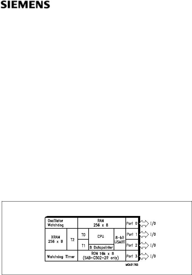
Figure 1 shows a block diagram of the SAB-C502.
Figure 1
Block Diagram of the SAB-C502
Semiconductor Group |
11 |

C502
CPU
The SAB-C502 is efficient both as a controller and as an arithmetic processor. It has extensive facilities for binary and BCD arithmetic and excels in its bit-handling capabilities. Efficient use of program memory results from an instruction set consisting of 44 % one-byte, 41 % two-byte, and 15 % three-byte instructions. With a 12 MHz crystal, 58 % of the instructions execute in 1.0 s (18 MHz : 667 ns).
Special Function Register PSW
Bit No. |
MSB |
|
|
|
|
|
|
LSB |
|
7 |
6 |
5 |
4 |
3 |
2 |
1 |
0 |
|
|
|
|
|
|
|
|
|
|
|
|
Addr. D0H |
CY |
AC |
F0 |
RS1 |
RS0 |
OV |
F1 |
P |
PSW |
Bit |
|
Function |
|
|
|
CY |
|
Carry Flag |
|
|
|
AC |
|
Auxiliary Carry Flag (for BCD operations) |
|
|
|
F0 |
|
General Purpose Flag |
|
|
|
RS1 |
RS0 |
Register Bank select control bits |
0 |
0 |
Bank 0 selected, data address 00H - 07H |
0 |
1 |
Bank 1 selected, data address 08H - 0FH |
1 |
0 |
Bank 2 selected, data address 10H - 17H |
1 |
1 |
Bank 3 selected, data address 18H - 1FH |
OV |
|
Overflow Flag |
|
|
|
F1 |
|
General Purpose Flag |
|
|
|
P |
|
Parity Flag. |
|
|
Set/cleared by hardware each instruction cycle to indicate an odd/ |
|
|
even number of “one” bits in the accumulator, i.e. even parity. |
|
|
|
Reset value of PSW is 00H.
Semiconductor Group |
12 |

C502
Special Function Registers
All registers, except the program counter and the four general purpose register banks, reside in the special function register area.
The 36 special function register (SFR) include pointers and registers that provide an interface between the CPU and the other on-chip peripherals. There are also 128 directly addressable bits within the SFR area.
All SFRs are listed in table 1, table 2 and table 3. In table 1 they are organized in numeric order of their addresses. In table 2 they are organized in groups which refer to the functional blocks of the SAB-C502. Table 3 illustrates the contents of the SFRs.
Table 1
Special Function Register in Numeric Order of their Addresses
Address |
Register |
Contents |
|
Address |
Register |
Contents |
|
||||||||||
|
|
|
after Reset |
|
|
|
|
after Reset |
|||||||||
|
|
|
|
|
|
|
|
|
|
|
|
|
|
|
|
||
80 |
H |
P0 1) |
FF |
H |
|
98 |
|
|
SCON 1) |
00 |
|
|
|
|
|||
81 |
|
|
|
|
H |
|
|
H |
|
|
|||||||
H |
SP |
07 |
|
|
|
99 |
|
|
SBUF |
XX |
H |
2) |
|
|
|||
82 |
|
|
H |
|
H |
|
|
|
|
|
|||||||
H |
DPL |
00 |
|
|
|
9A |
|
|
reserved |
XX |
H |
2) |
|
|
|||
83 |
|
|
H |
|
|
H |
|
|
|
|
|
||||||
H |
DPH |
00 |
|
|
|
9B |
|
|
reserved |
XX |
H |
2) |
|
|
|||
|
|
|
H |
|
|
H |
|
|
|
|
|
||||||
84H |
reserved |
|
|
|
|
|
9CH |
reserved |
XXH 2) |
|
|
||||||
85H |
reserved |
|
|
|
|
|
9DH |
reserved |
XXH 2) |
|
|
||||||
86 |
H |
WDTREL |
00 |
|
|
|
9E |
|
|
reserved |
XX |
H |
2) |
|
|
||
87 |
|
|
H |
|
|
H |
|
|
|
|
|
||||||
H |
PCON |
000X0000 |
2) |
9F |
H |
reserved |
XX |
H |
2) |
|
|
||||||
|
|
|
|
|
B |
|
|
|
|
|
|
|
|||||
88 |
H |
TCON 1) |
00 |
|
|
|
A0 |
H |
P2 1) |
FF |
H |
|
|
||||
|
|
|
H |
|
|
|
|
|
|
|
|||||||
89 |
H |
TMOD |
00 |
|
|
|
A1 |
|
|
reserved |
XX |
H |
2) |
|
|
||
|
|
|
H |
|
|
H |
|
|
|
|
|
||||||
8A |
|
TL0 |
00 |
|
|
|
A2 |
|
|
reserved |
XX |
H |
2) |
|
|
||
|
H |
|
|
H |
|
|
H |
|
|
|
|
|
|||||
8B |
|
TL1 |
00 |
|
|
|
A3 |
|
|
reserved |
XX |
H |
2) |
|
|
||
|
H |
|
|
H |
|
|
H |
|
|
|
|
|
|||||
8C |
H |
TH0 |
00 |
|
|
|
A4 |
|
|
reserved |
XX |
H |
2) |
|
|
||
|
|
|
H |
|
|
H |
|
|
|
|
|
||||||
8D |
H |
TH1 |
00 |
|
|
|
A5 |
|
|
reserved |
XX |
H |
2) |
|
|
||
|
|
|
H |
|
|
H |
|
|
|
|
|
||||||
8E |
|
reserved |
XX |
H |
2) |
|
A6 |
|
|
reserved |
XX |
H |
2) |
|
|
||
|
H |
|
|
|
|
|
H |
|
|
|
|
|
|||||
8F |
|
reserved |
XX |
H |
2) |
|
A7 |
|
|
reserved |
XX |
H |
2) |
|
|
||
|
H |
|
|
|
|
|
H |
|
|
|
|
|
|||||
90 |
H |
P1 1) |
FF |
H |
|
A8 |
H |
IE 1) |
0X000000 |
B |
2) |
||||||
91 |
XPAGE |
00 |
|
A9 |
reserved |
XX |
|
|
2) |
|
|||||||
H |
|
|
|
|
|
H |
|
|
|||||||||
|
|
|
H |
|
|
H |
|
|
|
|
|
||||||
92 |
H |
DPSEL |
XXXXX000 |
2) |
AA |
H |
SRELL |
D9 |
|
|
|
||||||
|
|
|
|
|
B |
|
|
|
|
H |
|
|
|||||
93H |
reserved |
XXH 2) |
|
ABH |
reserved |
XXH 2) |
|
|
|||||||||
94 |
H |
XCON |
F8 |
|
|
|
AC |
H |
reserved |
XX |
H |
2) |
|
|
|||
|
|
|
H |
|
|
|
|
|
|
|
|
||||||
95H |
reserved |
XXH 2) |
|
ADH |
reserved |
XXH 2) |
|
|
|||||||||
96H |
reserved |
XXH 2) |
|
AEH |
reserved |
XXH 2) |
|
|
|||||||||
97H |
reserved |
XXH 2) |
|
AFH |
reserved |
XXH 2) |
|
|
|||||||||
1): Bit-addressable Special Function Register
2): X means that the value is indeterminate and the location is reserved
Semiconductor Group |
13 |
 Loading...