


Siemens SAB80C535-16-N-T40-85, SAB80C535-20-N, SAB80C535-M, SAB80C535-M-T40-85, SAB80C535-N Datasheet
...Microcomputer Components
8-Bit CMOS Single-Chip Microcontroller
SAB 80C515 / SAB 80C535
Data Sheet 02.96

High-Performance |
|
8-Bit CMOS Single-Chip Microcontroller |
SAB 80C515/80C535 |
Preliminary
SAB 80C515/80C515-16 CMOS microcontroller with factory mask-programmable ROM SAB 80C535/80C535-16 CMOS microcontroller for external ROM
●8 K × 8 ROM (SAB 80C515 only)
●256 × 8 RAM
●Six 8-bit I/O ports, one input port for digital or analog input
●Three 16-bit timer/counters
●Highly flexible reload, capture, compare capabilities
●Full-duplex serial channel
●Twelve interrupt vectors, four priority levels
●8-bit A/D converter with 8 multiplexed inputs and programmable internal reference voltages
●16-bit watchdog timer
●Boolean processor
●Most instructions execute in 1 μs (750 ns)
●4 μs (3 μs) multiply and divide
●External memory expandable up to 128 Kbytes
●Backwardly compatible with SAB 8051
●Functionally compatible with SAB 80515
●Idle and power-down mode
●Plastic leaded chip carrier package: P-LCC-68
●Plastic Metric Quad Flat Package P-MQFP-80
●Two temperature ranges available:
0 to 70 |
˚C |
(for 12, |
16, 20 MHz) |
– 40 to |
85 ˚C |
(for 12, |
16 MHz) |
The SAB 80C515/80C535 is a powerful member of the Siemens SAB 8051 family
of 8-bit microcontrollers. It is designed in Siemens ACMOS technology and is functionally compatible with the SAB 80515/80535 devices designed in MYMOS technology.
The SAB 80C515/80C535 is a stand-alone, high-performance single-chip microcontroller based on the SAB 8051/80C51 architecture. While maintaining all the SAB 80C51 operating characteristics, the SAB 80C515/80C535 incorporates several enhancements which significantly increase design flexibility and overall system performance.
In addition, the low-power properties of Siemens ACMOS technology allow applications where power consumption and dissipation are critical. Furthermore, the SAB 80C515/80C535 has two software-selectable modes of reduced activity for further power reduction: idle and powerdown mode.
The SAB 80C535 is identical with the SAB 80C515 except that it lacks the on-chip program memory. The SAB 80C515/80C535 is supplied in a 68-pin plastic leaded chip carrier package (P-LCC-68) or in a plastic metric quad flat package (P-MQFP-80).
There are versions for 12, 16 and 20 MHz operation and for 16 MHz operation and for extended temperature ranges – 40 to 85 ˚C. Versions for extended temperature range – 40 to + 110 ˚C are available on request.
Semiconductor Group |
1 |
02.96 |
SAB 80C515/80C535
Semiconductor Group |
2 |

SAB 80C515/80C535
Ordering Information
Type |
Ordering |
Package |
Description |
|
Code |
|
8-Bit CMOS Microcontroller |
|
|
|
|
SAB 80C515-N |
Q67120-DXXXX |
P-LCC-68 |
with mask-programmable ROM, |
|
|
|
12 MHz |
|
|
|
|
SAB 80C535-N |
Q67120-C0508 |
P-LCC-68 |
for external memory, 12 MHz |
|
|
|
|
SAB 80C515-N-T40/85 |
Q67120-DXXXX |
P-LCC-68 |
with mask-programmable ROM, |
|
|
|
12 MHz |
|
|
|
ext. temperature – 40 to + 85 ˚C |
|
|
|
|
SAB 80C535-N-T40/85 |
Q67120-C0510 |
P-LCC-68 |
for external memory, 12 MHz |
|
|
|
ext. temperature – 40 to + 85 ˚C |
|
|
|
|
SAB 80C515-16-N |
Q67120-DXXXX |
P-LCC-68 |
with mask-programmable ROM, |
|
|
|
16 MHz |
|
|
|
|
SAB 80C535-16-N |
Q67120-C0509 |
P-LCC-68 |
for external memory, 16 MHz |
|
|
|
|
SAB 80C535-16-N- |
Q67120-C0562 |
P-LCC-68 |
for external memory, 16 MHz |
T40/85 |
|
|
ext. temperature – 40 to + 85 ˚C |
|
|
|
|
SAB 80C535-20-N |
Q67120-C0778 |
P-LCC-68 |
for external memory, 20 MHz |
|
|
|
|
SAB 80C535-M |
Q67120-C0857 |
P-MQFP-80 |
for external memory, 12 MHz |
|
|
|
|
SAB 80C515-M |
Q67120-DXXXX |
P-MQFP-80 |
with mask-programmable ROM, |
|
|
|
12 MHz |
|
|
|
|
SAB 80C535-M-T40/85 |
Q67120-C0937 |
P-MQFP-80 |
for external memory, 12 MHz |
|
|
|
ext. temperature – 40 to + 85 ˚C |
|
|
|
|
SAB 80C515-M-T40/85 |
Q67120-DXXXX |
P-MQFP-80 |
with mask-programmable ROM, |
|
|
|
12 MHz |
|
|
|
ext. temperature – 40 to + 85 ˚C |
|
|
|
|
Notes: Versions for extended temperature range – 40 to + 110 ˚C on request.
The ordering number of ROM types (DXXXX extension) is defined after program release (verification) of the customer.
Semiconductor Group |
3 |
SAB 80C515/80C535
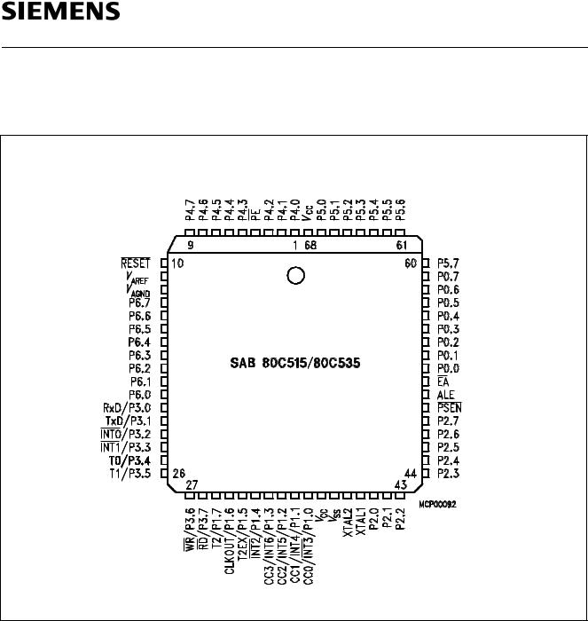
Pin Configuration
(top view)
P-LCC-68
Semiconductor Group |
4 |
SAB 80C515/80C535
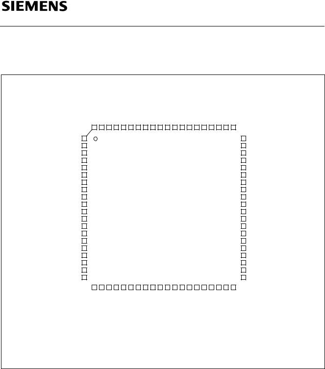
Pin Configuration
(top view)
P-MQFP-80
|
|
|
|
|
|
P4.7 |
|
P4.6 |
P4.5 |
P4.4 |
P4.3 |
|
PE |
|
P4.2 |
P4.1 |
P4.0 N.C. N.C. VCC N.C. |
P5.0 |
P5.1 |
P5.2 |
P5.3 |
P5.4 |
P5.5 |
P5.6 |
|
|
|
|
|
||
|
|
|
|
|
|
|
|
|
|
|
|
|
|
||||||||||||||||||
|
|
|
|
|
|
|
|
|
|
|
|
|
|
|
|
|
|
|
|
|
|
|
|
|
|
|
|
|
|
|
|
|
|
|
|
|
80 |
|
|
|
|
|
75 |
|
|
|
70 |
|
|
65 |
|
|
|
61 |
|
|
|
|
|
||||
|
RESET |
|
|
1 |
|
|
|
|
|
|
|
|
|
|
|
|
|
|
|
|
|
|
|
|
60 |
|
P5.7 |
|
|
||
|
|
|
|
|
|
|
|
|
|
|
|
|
|
|
|
|
|
|
|
|
|
|
|||||||||
|
|
N.C. |
|
|
|
|
|
|
|
|
|
|
|
|
|
|
|
|
|
|
|
|
|
|
|
|
P0.7 |
/ AD7 |
|||
|
VAREF |
|
|
|
|
|
|
|
|
|
|
|
|
|
|
|
|
|
|
|
|
|
|
|
|
P0.6 |
/ AD6 |
||||
VAGND |
|
|
|
|
|
|
|
|
|
|
|
|
|
|
|
|
|
|
|
|
|
|
|
|
P0.5 |
/ AD5 |
|||||
P6.7 / AIN7 |
|
5 |
|
|
|
|
|
|
|
|
|
|
|
|
|
|
|
|
|
|
|
|
|
|
P0.4 |
/ AD4 |
|||||
P6.6 / AIN6 |
|
|
|
|
|
|
|
|
|
|
|
|
|
|
|
|
|
|
|
|
|
|
55 |
|
P0.3 |
/ AD3 |
|||||
P6.5 / AIN5 |
|
|
|
|
|
|
|
|
|
|
|
|
|
|
|
|
|
|
|
|
|
|
|
|
P0.2 |
/ AD2 |
|||||
P6.4 / AIN4 |
|
|
|
|
|
|
|
|
|
SAB 80C535 / 80C515 |
|
|
|
|
|
|
P0.1 |
/ AD1 |
|||||||||||||
P6.3 / AIN3 |
|
|
|
|
|
|
|
|
|
|
|
|
|
|
|
P0.0 |
/ AD0 |
||||||||||||||
|
|
|
|
|
|
|
|
|
|
|
|
|
|
|
|
|
|
|
|
|
|
|
|
||||||||
P6.2 / AIN2 |
|
10 |
|
|
|
|
|
|
|
|
|
P-MQFP-80 |
|
|
|
|
|
|
|
|
N.C. |
|
|
||||||||
P6.1 / AIN1 |
|
|
|
|
|
|
|
|
|
|
|
|
|
|
|
|
|
|
50 |
|
N.C. |
|
|
||||||||
|
|
|
|
|
|
|
|
|
|
|
|
|
Package |
|
|
|
|
|
|
|
|
|
|||||||||
P6.0 / AIN0 |
|
|
|
|
|
|
|
|
|
|
|
|
|
|
|
|
|
|
|
|
|
EA |
|
|
|
||||||
|
|
N.C. |
|
|
|
|
|
|
|
|
|
|
|
|
|
|
|
|
|
|
|
|
|
|
|
|
ALE |
|
|
||
|
|
N.C. |
|
|
|
|
|
|
|
|
|
|
|
|
|
|
|
|
|
|
|
|
|
|
|
|
PSEN |
|
|||
P3.0 / RXD0 |
|
15 |
|
|
|
|
|
|
|
|
|
|
|
|
|
|
|
|
|
|
|
|
|
N.C. |
|
|
|||||
P3.1 / TXD0 |
|
|
|
|
|
|
|
|
|
|
|
|
|
|
|
|
|
|
|
|
|
|
45 |
|
P2.7 |
/ A15 |
|||||
P3.2 / |
INT0 |
|
|
|
|
|
|
|
|
|
|
|
|
|
|
|
|
|
|
|
|
|
|
|
|
|
P2.6 |
/ A14 |
|||
P3.3 / |
INT1 |
|
|
|
|
|
|
|
|
|
|
|
|
|
|
|
|
|
|
|
|
|
|
|
|
|
P2.5 |
/ A13 |
|||
P3.4 / T0 |
|
|
|
|
|
|
|
|
|
|
|
|
|
|
|
|
|
|
|
|
|
|
|
|
P2.4 |
/ A12 |
|||||
P3.5 / T1 |
|
20 |
|
|
|
|
25 |
|
|
|
|
|
30 |
|
|
|
35 |
|
|
|
|
41 |
|
P2.3 |
/ A11 |
||||||
|
|
|
|
|
21 |
|
|
|
|
|
|
|
|
|
|
|
|
|
|
|
|
40 |
|
|
|
|
|
||||
|
|
|
|
|
|
P3.6 / WR |
|
P3.7 / RD |
N.C. |
P1.7 / T2 |
P1.6 / CLKOUT |
|
P1.5 / T2EX |
|
P1.4 / INT2 |
P1.3 / INT6 / CC3 |
P1.2 / INT5 / CC2 P1.1 / INT4 / CC1 |
|
P1.0 / INT3 / CC0 N.C. VCC |
VSS |
N.C. |
XTAL2 |
XTAL1 |
P2.0 / A8 |
P2.1 / A9 |
P2.2 / A10 |
|
|
|
|
|
|
|
|
|
|
|
|
|
|
|
|
|
|
|
|
|||||||||||||||||
|
|
|
|
|
|
|
|
|
|
|
|
|
|||||||||||||||||||
|
|
|
|
|
|
|
|
|
|
|
|
|
|
|
|
||||||||||||||||
|
|
|
|
|
|
|
|
|
|
|
|
|
|
|
|
|
|||||||||||||||
|
|
|
|
|
|
|
|
|
|
|
|
|
|
|
|
|
|
|
|
|
|
|
|
|
|||||||
N.C. pins must not be connected.
Semiconductor Group |
5 |
SAB 80C515/80C535
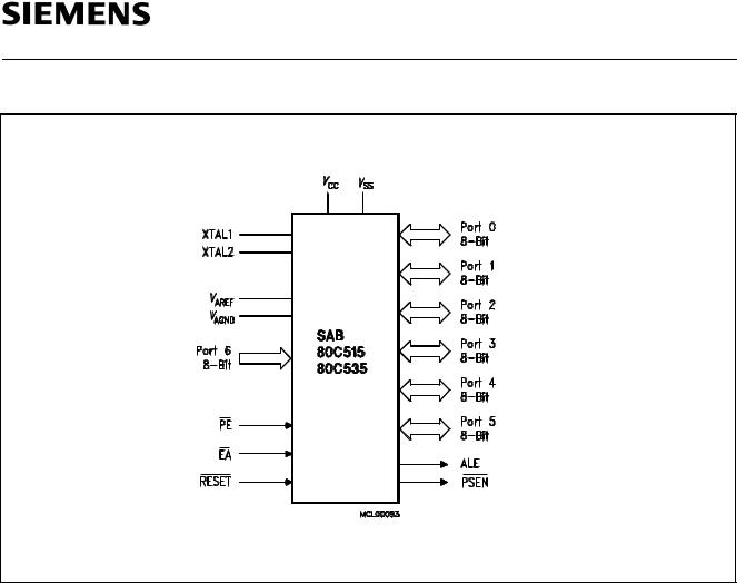
Logic Symbol
Semiconductor Group |
6 |

SAB 80C515/80C535
Pin Definitions and Functions
Symbol |
Pin |
Pin |
Input (I) |
Function |
|||||
|
|
|
P-LCC-68 |
P-MQFP-80 |
Output (O) |
|
|
|
|
|
|
|
|
|
|||||
P4.0-P4.7 |
1-3, 5-9 |
72-74, |
I/O |
Port 4 |
|||||
|
|
|
|
76-80 |
|
is an 8-bit bidirectional I/O port with |
|||
|
|
|
|
|
|
internal pullup resistors. Port 4 pins that |
|||
|
|
|
|
|
|
have 1’s written to them are pulled high by |
|||
|
|
|
|
|
|
the internal pullup resistors, and in that |
|||
|
|
|
|
|
|
state can be used as inputs. As inputs, |
|||
|
|
|
|
|
|
port 4 pins being externally pulled low will |
|||
|
|
|
|
|
|
source current (II L, in the DC |
|||
|
|
|
|
|
|
|
characteristics) because of the internal |
||
|
|
|
|
|
|
|
pullup resistors. |
||
|
|
|
|
|
|
|
|
|
|
|
|
|
4 |
75 |
I |
|
|
|
|
PE |
|
|
Power saving mode enable |
||||||
|
|
|
|
|
|
A low level on this pin enables the use of |
|||
|
|
|
|
|
|
the power saving modes (idle mode and |
|||
|
|
|
|
|
|
power-down mode). When PE is held on |
|||
|
|
|
|
|
|
high level it is impossible to enter the |
|||
|
|
|
|
|
|
power saving modes. |
|||
|
|
|
|
|
|
|
|||
|
|
|
10 |
1 |
I |
|
|
pin |
|
RESET |
|
Reset |
|||||||
|
|
|
|
|
|
A low level on this pin for the duration of |
|||
|
|
|
|
|
|
two machine cycles while the oscillator is |
|||
|
|
|
|
|
|
running resets the SAB 80C515. A small |
|||
|
|
|
|
|
|
internal pullup resistor permits power-on |
|||
|
|
|
|
|
|
reset using only a capacitor connected |
|||
|
|
|
|
|
|
|
to VSS. |
||
VAREF |
11 |
3 |
|
Reference voltage for the A/D converter |
|||||
|
|
|
|
|
|||||
VAGND |
12 |
4 |
|
Reference ground for the A/D converter |
|||||
|
|
|
|
|
|||||
P6.7-P6.0 |
13-20 |
5-12 |
|
Port 6 |
|||||
|
|
|
|
|
|
is an 8-bit undirectional input port. Port |
|||
|
|
|
|
|
|
pins can be used for digital input if voltage |
|||
|
|
|
|
|
|
levels simultaneously meet the |
|||
|
|
|
|
|
|
specifications for high/low input voltages |
|||
|
|
|
|
|
|
and for the eight multiplexed analog inputs |
|||
|
|
|
|
|
|
of the A/D converter. |
|||
|
|
|
|
|
|
|
|
|
|
Semiconductor Group |
7 |

SAB 80C515/80C535
Pin Definitions and Functions (cont’d)
Symbol |
Pin |
Pin |
Input (I) |
Function |
|||||||
|
P-LCC-68 |
P-MQFP-80 |
Output (O) |
|
|
|
|
|
|
|
|
|
|
|
|
|
|||||||
P3.0-P3.7 |
21-28 |
15-22 |
I/O |
Port 3 |
|||||||
|
|
|
|
is an 8-bit bidirectional I/O port with |
|||||||
|
|
|
|
internal pullup resistors. Port 3 pins that |
|||||||
|
|
|
|
have1's written to them are pulled high by |
|||||||
|
|
|
|
the internal pullup resistors, and in that |
|||||||
|
|
|
|
state can be used as inputs. As inputs, |
|||||||
|
|
|
|
port 3 pins being externally pulled low will |
|||||||
|
|
|
|
source current (IIL, in the DC |
|||||||
|
|
|
|
characteristics) because of the internal |
|||||||
|
|
|
|
pullup resistors. Port 3 also contains the |
|||||||
|
|
|
|
interrupt, timer, serial port and external |
|||||||
|
|
|
|
memory strobe pins that are used by |
|||||||
|
|
|
|
various options. The output latch |
|||||||
|
|
|
|
corresponding to a secondary function |
|||||||
|
|
|
|
must be programmed to a one (1) for that |
|||||||
|
|
|
|
function to operate. The secondary |
|||||||
|
|
|
|
functions are assigned to the pins of port |
|||||||
|
|
|
|
3, as follows: |
|||||||
|
|
|
|
– R×D (P3.0): serial port's receiver data |
|||||||
|
|
|
|
|
input (asynchronous) or data input/ |
||||||
|
|
|
|
|
output (synchronous) |
||||||
|
|
|
|
– T×D (P3.1): serial port's transmitter data |
|||||||
|
|
|
|
|
|
output |
|||||
|
|
|
|
|
|
(asynchronous) or clock output |
|||||
|
|
|
|
|
|
(synchronous) |
|||||
|
|
|
|
|
|
|
|
|
|
||
|
|
|
|
– |
INT0 |
(P3.2): interrupt 0 input/timer 0 |
|||||
|
|
|
|
|
|
gate control input |
|||||
|
|
|
|
|
|
|
|
||||
|
|
|
|
– |
INT1 |
(P3.3): interrupt 1 input/timer 1 |
|||||
|
|
|
|
|
gate control input |
||||||
|
|
|
|
– T0 (P3.4): counter 0 input |
|||||||
|
|
|
|
– T1 (P3.5): counter 1 input |
|||||||
|
|
|
|
|
|
||||||
|
|
|
|
– |
WR |
(P3.6): the write control signal |
|||||
|
|
|
|
|
latches the data byte from port 0 into the |
||||||
|
|
|
|
|
external data memory |
||||||
|
|
|
|
|
|||||||
|
|
|
|
– |
RD |
(P3.7): the read control signal |
|||||
|
|
|
|
|
enables the external data memory to |
||||||
|
|
|
|
|
port 0 |
||||||
|
|
|
|
|
|
|
|
|
|
|
|
Semiconductor Group |
8 |

SAB 80C515/80C535
Pin Definitions and Functions (cont’d)
Symbol |
Pin |
Pin |
Input (I) |
Function |
||
|
P-LCC-68 |
P-MQFP-80 |
Output (O) |
|
|
|
|
|
|
|
|
||
P1.7-P1.0 |
29-36 |
24-31 |
I/O |
Port 1 |
||
|
|
|
|
is an 8-bit bidirectional I/O port with |
||
|
|
|
|
internal pullup resistors. Port 1 pins that |
||
|
|
|
|
have 1's written to them are pulled high by |
||
|
|
|
|
the internal pullup resistors, and in that |
||
|
|
|
|
state can be used as inputs. As inputs, |
||
|
|
|
|
port 1 pins being externally pulled low will |
||
|
|
|
|
source current (II L in the DC |
||
|
|
|
|
characteristics) because of the internal |
||
|
|
|
|
pullup resistors. The port is used for the |
||
|
|
|
|
low-order address byte during program |
||
|
|
|
|
verification. Port 1 also contains the |
||
|
|
|
|
interrupt, timer, clock, capture and |
||
|
|
|
|
compare pins that are used by various |
||
|
|
|
|
options. The output latch corresponding to |
||
|
|
|
|
a secondary function must be |
||
|
|
|
|
programmed to a one (1) for that function |
||
|
|
|
|
to operate (except when used for the |
||
|
|
|
|
compare functions). The secondary |
||
|
|
|
|
functions are assigned to the port 1 pins |
||
|
|
|
|
as follows: |
||
|
|
|
|
|
|
|
|
|
|
|
– |
INT3/CC0 (P1.0): interrupt 3 input/ |
|
|
|
|
|
|
compare 0 output/capture 0 input |
|
|
|
|
|
– INT4/CC1 (P1.1): interrupt 4 input/ |
||
|
|
|
|
|
compare 1 output/capture 1 input |
|
|
|
|
|
– INT5/CC2 (P1.2): interrupt 5 input/ |
||
|
|
|
|
|
compare 2 output/capture 2 input |
|
|
|
|
|
– INT6/CC3 (P1.3): interrupt 6 input/ |
||
|
|
|
|
|
compare 3 output/capture 3 input |
|
|
|
|
|
|
||
|
|
|
|
– |
INT2 |
(P1.4): interrupt 2 input |
|
|
|
|
– T2EX (P1.5): timer 2 external reload |
||
|
|
|
|
|
trigger input |
|
|
|
|
|
– CLKOUT (P1.6): system clock output |
||
|
|
|
|
– T2 (P1.7): counter 2 input |
||
|
|
|
|
|
|
|
Semiconductor Group |
9 |
SAB 80C515/80C535
Pin Definitions and Functions (cont’d)
Symbol |
Pin |
Pin |
Input (I) |
Function |
|
P-LCC-68 |
P-MQFP-80 |
Output (O) |
|
|
|
|
|
|
XTAL2 |
39 |
36 |
|
XTAL2 |
XTAL1 |
40 |
37 |
|
Input to the inverting oscillator amplifier |
|
|
|
|
and input to the internal clock generator |
|
|
|
|
circuits. |
|
|
|
|
XTAL1 |
|
|
|
|
Output of the inverting oscillator amplifier. |
|
|
|
|
To drive the device from an external clock |
|
|
|
|
source, XTAL2 should be driven, while |
|
|
|
|
XTAL1 is left unconnected. There are no |
|
|
|
|
requirements on the duty cycle of the |
|
|
|
|
external clock signal, since the input to the |
|
|
|
|
internal clocking circuitry is divided down |
|
|
|
|
by a divide-by-two flip-flop. Minimum and |
|
|
|
|
maximum high and low times and rise/fall |
|
|
|
|
times specified in the AC characteristics |
|
|
|
|
must be observed. |
|
|
|
|
|
P2.0-P2.7 |
41-48 |
38-45 |
I/O |
Port 2 |
|
|
|
|
is an 8-bit bidirectional I/O port with |
|
|
|
|
internal pullup resistors. Port 2 pins that |
|
|
|
|
have 1's written to them are pulled high by |
|
|
|
|
the internal pullup resistors, and in that |
|
|
|
|
state can be used as inputs. As inputs, |
|
|
|
|
port 2 pins being externally pulled low will |
|
|
|
|
source current (I I L, in the DC |
|
|
|
|
characteristics) because of the internal |
|
|
|
|
pullup resistors. |
|
|
|
|
Port 2 emits the high-order address byte |
|
|
|
|
during fetches from external program |
|
|
|
|
memory and during accesses to external |
|
|
|
|
data memory that use 16-bit addresses |
|
|
|
|
(MOVX@DPTR). In this application it |
|
|
|
|
uses strong internal pullup resistors when |
|
|
|
|
issuing 1's. During accesses to external |
|
|
|
|
data memory that use 8-bit addresses |
|
|
|
|
(MOVX@Ri), port 2 issues the contents of |
|
|
|
|
the P2 special function register. |
|
|
|
|
|
Semiconductor Group |
10 |

SAB 80C515/80C535
Pin Definitions and Functions (cont’d)
Symbol |
Pin |
Pin |
Input (I) |
Function |
||||||
|
|
|
P-LCC-68 |
P-MQFP-80 |
Output (O) |
|
|
|
|
|
|
|
|
|
|
|
|
|
|
||
|
|
|
49 |
47 |
O |
The |
|
|
|
|
PSEN |
|
Program store enable |
||||||||
|
|
|
|
|
|
output is a control signal that enables the |
||||
|
|
|
|
|
|
external program memory to the bus |
||||
|
|
|
|
|
|
during external fetch operations. It is |
||||
|
|
|
|
|
|
activated every six oscillator periods, |
||||
|
|
|
|
|
|
except during external data memory |
||||
|
|
|
|
|
|
accesses. The signal remains high during |
||||
|
|
|
|
|
|
internal program execution. |
||||
|
|
|
|
|
||||||
ALE |
50 |
48 |
O |
The Address latch enable |
||||||
|
|
|
|
|
|
|
output is used for latching the address into |
|||
|
|
|
|
|
|
|
external memory during normal operation. |
|||
|
|
|
|
|
|
|
It is activated every six oscillator periods, |
|||
|
|
|
|
|
|
|
except during an external data memory |
|||
|
|
|
|
|
|
|
access. |
|||
|
|
|
|
|
|
|
||||
|
|
|
51 |
49 |
I |
|
|
|
|
|
EA |
|
External access enable |
||||||||
|
|
|
|
|
|
When held high, the SAB 80C515 |
||||
|
|
|
|
|
|
executes instructions from the internal |
||||
|
|
|
|
|
|
ROM as long as the PC is less than 8192. |
||||
|
|
|
|
|
|
When held low, the SAB 80C515 fetches |
||||
|
|
|
|
|
|
all instructions from external program |
||||
|
|
|
|
|
|
memory. For the SAB 80C535 this pin |
||||
|
|
|
|
|
|
must be tied low. |
||||
|
|
|
|
|
||||||
P0.0-P0.7 |
52-59 |
52-59 |
I/O |
Port 0 |
||||||
|
|
|
|
|
|
is an 8-bit open-drain bidirectional I/O |
||||
|
|
|
|
|
|
port. |
||||
|
|
|
|
|
|
Port 0 pins that have 1's written to them |
||||
|
|
|
|
|
|
float, and in that state can be used as |
||||
|
|
|
|
|
|
high-impedance inputs. |
||||
|
|
|
|
|
|
Port 0 is also the multiplexed low-order |
||||
|
|
|
|
|
|
address and data bus during accesses to |
||||
|
|
|
|
|
|
external program and data memory. In |
||||
|
|
|
|
|
|
this application it uses strong internal |
||||
|
|
|
|
|
|
pullup resistors when issuing 1's. |
||||
|
|
|
|
|
|
Port 0 also outputs the code bytes during |
||||
|
|
|
|
|
|
program verification in the SAB 80C515. |
||||
|
|
|
|
|
|
External pullup resistors are required |
||||
|
|
|
|
|
|
during program verification. |
||||
|
|
|
|
|
|
|
|
|
|
|
Semiconductor Group |
11 |

SAB 80C515/80C535
Pin Definitions and Functions (cont’d)
Symbol |
Pin |
Pin |
Input (I) |
Function |
|
P-LCC-68 |
P-MQFP-80 |
Output (O) |
|
|
|
|
|
|
P5.7-P5.0 |
60-67 |
60-67 |
I/O |
Port 5 is an 8-bit bidirectional I/O port with |
|
|
|
|
internal pullup resistors. Port 5 pins that |
|
|
|
|
have 1's written to them are pulled high by |
|
|
|
|
the internal pullup resistors, and in that |
|
|
|
|
state can be used as inputs. As inputs, |
|
|
|
|
port 5 pins being externally pulled low will |
|
|
|
|
source current |
|
|
|
|
(I IL in the DC characteristics) because of |
|
|
|
|
the internal pullup resistors. |
|
|
|
|
|
VCC |
37 |
33 |
– |
Supply voltage |
|
|
|
|
during normal, idle, and power-down |
|
|
|
|
operation. Internally connected to pin 68. |
|
|
|
|
|
VSS |
38 |
34 |
– |
Ground (0 V) |
VCC |
68 |
69 |
– |
Supply voltage |
|
|
|
|
during normal, idle, and power-down |
|
|
|
|
operation. Internally connected to pin 37. |
|
|
|
|
|
N. C. |
– |
2, 13, 14, |
– |
Not connected |
|
|
23, 32, 35, |
|
These pins of the P-MQFP-80 package |
|
|
46, 50, 51, |
|
must not be connected |
|
|
68, 70, 71 |
|
|
|
|
|
|
|
Semiconductor Group |
12 |

SAB 80C515/80C535
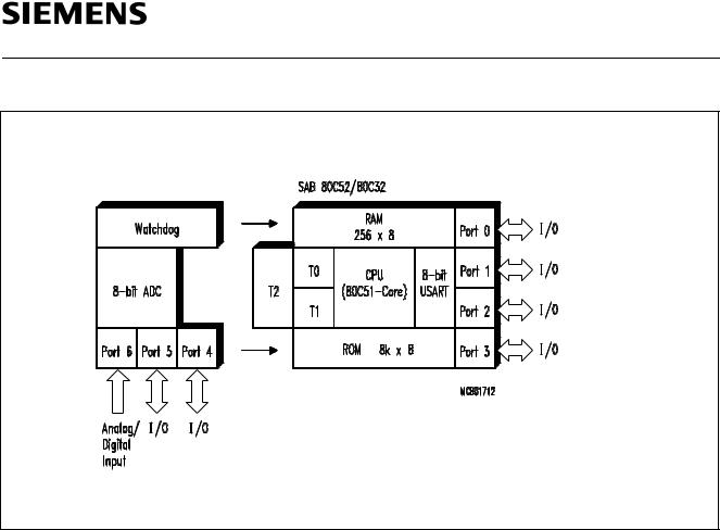
Figure 1
Block Diagram
Semiconductor Group |
13 |

SAB 80C515/80C535
Functional Description
The members of the SAB 80515 family of microcontrollers are:
– SAB 80C515: Microcontroller, designed in Siemens ACMOS technology, with 8 Kbyte factory mask-programmable ROM
–SAB 80C535: ROM-less version of the SAB 80C515
–SAB 80515: Microcontroller, designed in Siemens MYMOS technology, with
8 Kbyte factory mask-programmable ROM
– SAB 80535: ROM-less version of the SAB 80515
The SAB 80C535 is identical to the SAB 80C515, except that it lacks the on-chip ROM. In this data sheet the term "SAB 80C515" is used to refer to both the SAB 80C515 and SAB 80C535, unless otherwise noted.
Principles of Architecture
The architecture of the SAB 80C515 is based on the SAB 8051/SAB 80C51 microcontroller family. The following features of the SAB 80C515 are fully compatible with the SAB 80C51 features:
–Instruction set
–External memory expansion interface (port 0 and port 2)
–Full-duplex serial port
–Timer/counter 0 and 1
–Alternate functions on port 3
–The lower 128 bytes of internal RAM and the lower 4 Kbytes of internal ROM
The SAB 80C515 additionally contains 128 bytes of internal RAM and 4 Kbytes of internal ROM, which results in a total of 256 bytes of RAM and 8 Kbytes of ROM on-chip.
The SAB 80C515 has a new 16-bit timer/counter with a 2:1 prescaler, reload mode, compare and capture capability. It also contains at 16-bit watchdog timer, an 8-bit A/D converter with programmable reference voltages, two additional quasi-bidirectional 8-bit ports, one 8-bit input port for analog or digital signals, and a programmable clock output (fOSC/12).
Furthermore, the SAB 80C515 has a powerful interrupt structure with 12 vectors and 4 programmable priority levels.
Figure 1 shows a block diagram of the SAB 80C515.
Semiconductor Group |
14 |

SAB 80C515/80C535
CPU
The SAB 80C515 is efficient both as a controller and as an arithmetic processor. It has extensive facilities for binary and BCD arithmetic and excels in its bit-handling capabilities. Efficient use of program memory results from an instruction set consisting of 44 % one-byte, 41 % two-byte, and 15 % three-byte instructions. With a 12 MHz crystal, 58 % of the instructions execute in 1.0 μs.
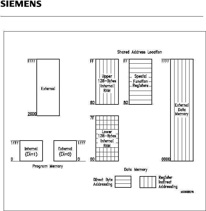
Memory Organization
The SAB 80C515 manipulates operands in the four memory address spaces described below: Figure 1 illustrates the memory address spaces of the SAB 80C515.
Program Memory
The SAB 80C515 has 8 Kbyte of on-chip ROM, while the SAB 80C535 has no internal ROM. The program memory can be externally expanded up to 64 Kbytes. If the EA pin is held high, the SAB 80C515 executes out of internal ROM unless the address exceeds 1FFFH. Locations
2000H through 0FFFFH are then fetched from the external program memory. If the EA pin is held now, the SAB 80C515 fetches all instructions from the external program memory. Since the SAB 80C535 has no internal ROM, pin EA must be tied low when using this component.
Data Memory
The data memory address space consists of an internal and an external memory space. The internal data memory is divided into three physically separate and distinct blocks:
the lower 128 bytes of RAM, the upper 128 bytes of RAM, and the 128 byte special function register (SRF) area. While the upper 128 bytes of data memory and the SFR area share the same address locations, they are accessed through different addressing modes. The lower 128 bytes of data memory can be accessed through direct or register indirect addressing; the upper 128 bytes of RAM can be accessed through register indirect addressing; the special function registers are accessible through direct addressing.
Four 8-register banks, each bank consisting of eight 8-bit multi-purpose registers, occupy locations 0 through 1FH in the lower RAM area. The next 16 bytes, locations 20H through 2FH, contain 128 directly addressable bit locations. The stack can be located anywhere in the internal data memory address space, and the stack depth can be expanded up to 256 bytes.
The external data memory can be expanded up to 64 Kbytes and can be accessed by instructions that use a 16-bit or an 8-bit address.
Semiconductor Group |
15 |
SAB 80C515/80C535
Figure 2
Memory Address Spaces
Semiconductor Group |
16 |
 Loading...