


Siemens SAB80C515A-M18-T3, SAB80C515A-N18, SAB80C515A-N18-T3, SAB83C515A-5M18-T3, SAB83C515A-5N18 Datasheet
...Microcomputer Components
8-Bit CMOS Single-Chip Microcontroller
SAB 80C515A/83C515A-5
Data Sheet 08.95

High-Performance |
SAB 80C515A / 83C515A-5 |
8-Bit CMOS Single-Chip Microcontroller |
|
Preliminary |
|
SAB 83C515A-5 |
Microcontroller with factory mask-programmable ROM |
SAB 80C515A |
Microcontroller for external ROM |
●SAB 80C515A / 83C515A-5, up to 18 MHz operation frequency
●32 K × 8 ROM (SAB 83C515A-5 only, ROM-Protection available)
●256 × 8 on-chip RAM
●Additional 1 K × 8 on-chip RAM (XRAM)
●Superset of SAB 80C51 architecture: 1 µs instruction cycle time at 12 MHz
666 ns instruction cycle time at 18 MHz
256 directly addressable bits Boolean processor
64 Kbyte external data and program memory addressing
●Three 16-bit timer/counters
●Versatile "fail-safe" provisions
●Twelve interrupt vectors, four priority levels selectable
●Genuine 10-bit A/D converter with 8 multiplexed inputs
●Full duplex serial interface with programmable Baudrate-Generator
●Functionally compatible with SAB 80C515
●Extended power saving mode
●Fast Power-On Reset
●Seven ports: 48 I/O lines, 8 input lines
●Two temperature ranges available: 0 to 70 °C (T1)
– 40 to 85 °C (T3)
●Plastic packages: P-LCC-68 and P-MQFP-80
The SAB 80C515A/83C515A-5 is a high-end member of the Siemens SAB 8051 microcontroller family. It is designed in Siemens ACMOS technology and based on the
SAB 8051 architecture. ACMOS is a technology which combines high-speed and density characteristics with low-power consumption or dissipation.
While maintaining all the SAB 80C515 features and operating characteristics the
SAB 80C515A/83C515A-5 contains more on-chip RAM/ROM. Furthermore a new 10-bit A/D- Converter is implemented as well as extended security mechanisms. The SAB 80C515A is identical with the SAB 83C515A-5 except that it lacks the on-chip program memory. The SAB 80C515A / 83C515A-5 is supplied in a 68-pin plastic leaded chip carrier package
(P-LCC- 68) and in a 80-pin plastic metric quad flat package (P-MQFP-80). Versions for extended temperature range – 40 to + 110 ∞C are available on request.
Semiconductor Group |
1 |
08.95 |

SAB 80C515A/83C515A-5 |
Ordering Information
Type |
Ordering |
Package |
Description |
|
Code |
|
8-Bit CMOS microcontroller |
|
|
|
|
SAB 80C515A-N18 |
Q67120-C0581 |
P-LCC-68 |
for external memory, 18 MHz |
|
|
|
|
SAB 83C515A-5N18 |
Q67120-DXXXX |
P-LCC-68 |
with mask-programmable ROM, |
|
|
|
18 MHz |
|
|
|
|
SAB 80C515A-N18-T3 |
Q67120-C0784 |
P-LCC-68 |
for external memory, 18 MHz |
|
|
|
ext. temperature − 40 to + 85 °C |
|
|
|
|
SAB 83C515A-5N18-T3 |
Q67120-DXXXX |
P-LCC-68 |
with mask-programmable ROM, |
|
|
|
18 MHz |
|
|
|
ext. temperature − 40 to + 85 °C |
|
|
|
|
SAB 80C515A-M18-T3 |
Q67120-C0851 |
P-MQFP-80 |
for external memory, 18 MHz |
|
|
|
ext. temperature − 40 to + 85 °C |
|
|
|
|
SAB 83C515A-5M18-T3 |
Q67120-DXXXX |
P-MQFP-80 |
with mask-programmable ROM, |
|
|
|
18 MHz |
|
|
|
ext. temperature − 40 to + 85 °C |
|
|
|
|
Notes: Versions for extended temperature range − 40 to + 110 °C on request.
The ordering number of ROM types (DXXXX extension) is defined after program release (verification) of the customer.
Semiconductor Group |
2 |

SAB 80C515A/83C515A-5
Logic Symbol
Semiconductor Group |
3 |

SAB 80C515A/83C515A-5
The pin functions of the SAB 80C515A are identical with those of the SAB 80C515 with following exception:
Pin |
|
|
SAB 80C515A |
|
SAB 80C515 |
|||||
|
|
|
|
|
|
|
|
|
||
68 |
|
|
|
|
|
|
|
VCC |
||
HWPD |
||||||||||
1 |
|
|
|
|
|
P4.0 |
||||
P0.4/ADST |
||||||||||
4 |
|
|
|
|
|
|
||||
PE/SWD |
PE |
|||||||||
|
|
|
|
|
|
|
|
|
|
|
|
|
|
|
|
|
|
|
|
|
|
|
|
|
|
|
|
|
|
|
|
|
Pin Configuration
(P-LCC-68)
Semiconductor Group |
4 |

SAB 80C515A/83C515A-5
|
|
|
|
|
|
P4.7 |
|
P4.6 |
P4.5 |
P4.4 |
P4.3 |
|
PE / SWD |
|
P4.2 |
P4.1 |
|
P4.0 / ADST |
N.C. |
|
N.C. |
|
HWPD |
N.C. |
P5.0 |
P5.1 |
P5.2 |
P5.3 |
P5.4 |
P5.5 |
P5.6 |
|
|
|
|
|
|
|
|
|
|
|
|
|
|
|
|
|
|
|
|
|
|
||||||||||||||||||||
|
|
|
|
|
|
|
|
|
|
|
|
|
|
|
||||||||||||||||||||||
|
|
|
|
|
|
|
|
|
|
|
|
|
|
|
|
|
|
|
|
|
|
|
|
|
|
|
|
|
|
|
|
|
|
|
|
|
|
|
|
|
|
|
80 |
|
|
|
|
75 |
|
|
|
|
|
|
70 |
|
|
|
|
|
65 |
|
|
|
61 |
|
P5.7 |
|
|
||||
|
RESET |
|
|
1 |
|
|
|
|
|
|
|
|
|
|
|
|
|
|
|
|
|
|
|
|
|
|
|
|
|
60 |
|
|
|
|||
|
|
N.C. |
|
|
|
|
|
|
|
|
|
|
|
|
|
|
|
|
|
|
|
|
|
|
|
|
|
|
|
|
P0.7 |
/ AD7 |
||||
|
VAREF |
|
|
|
|
|
|
|
|
|
|
|
|
|
|
|
|
|
|
|
|
|
|
|
|
|
|
|
|
P0.6 |
/ AD6 |
|||||
VAGND |
|
|
|
|
|
|
|
|
|
|
|
|
|
|
|
|
|
|
|
|
|
|
|
|
|
|
|
|
P0.5 |
/ AD5 |
||||||
P6.7 / AIN7 |
5 |
|
|
|
|
|
|
|
|
|
|
|
|
|
|
|
|
|
|
|
|
|
|
|
|
|
|
|
P0.4 |
/ AD4 |
||||||
P6.6 / AIN6 |
|
|
|
|
|
|
|
|
|
|
|
|
|
|
|
|
|
|
|
|
|
|
|
|
|
|
55 |
|
P0.3 |
/ AD3 |
||||||
P6.5 / AIN5 |
|
|
|
|
|
|
|
|
|
|
|
|
|
|
|
|
|
|
|
|
|
|
|
|
|
|
|
|
P0.2 |
/ AD2 |
||||||
P6.4 / AIN4 |
|
|
|
|
|
|
|
|
|
|
|
|
|
|
|
|
|
|
|
|
|
|
|
|
|
|
|
|
P0.1 |
/ AD1 |
||||||
P6.3 / AIN3 |
|
|
|
|
|
|
|
|
|
|
|
|
|
|
|
|
|
|
|
|
|
|
|
|
|
|
|
|
P0.0 |
/ AD0 |
||||||
P6.2 / AIN2 |
10 |
|
|
|
|
SAB 80C515A / 80C515A-5 |
|
|
|
|
|
N.C. |
|
|
||||||||||||||||||||||
P6.1 / AIN1 |
|
|
|
|
|
|
|
|
|
|
|
|
|
|
|
|
|
|
|
|
|
|
|
|
|
|
50 |
|
N.C. |
|
|
|||||
P6.0 / AIN0 |
|
|
|
|
|
|
|
|
|
|
|
|
|
|
|
|
|
|
|
|
|
|
|
|
|
|
|
|
|
|
|
|
||||
|
|
|
|
|
|
|
|
|
|
|
|
|
|
|
|
|
|
|
|
|
|
|
|
|
|
|
|
EA |
|
|
||||||
|
|
N.C. |
|
|
|
|
|
|
|
|
|
|
|
|
|
|
|
|
|
|
|
|
|
|
|
|
|
|
|
|
ALE |
|
|
|||
|
|
N.C. |
|
|
|
|
|
|
|
|
|
|
|
|
|
|
|
|
|
|
|
|
|
|
|
|
|
|
|
|
|
|
||||
|
|
|
|
|
|
|
|
|
|
|
|
|
|
|
|
|
|
|
|
|
|
|
|
|
|
|
|
PSEN |
||||||||
P3.0 / RXD0 |
15 |
|
|
|
|
|
|
|
|
|
|
|
|
|
|
|
|
|
|
|
|
|
|
|
|
|
|
N.C. |
|
|
||||||
P3.1 / TXD0 |
|
|
|
|
|
|
|
|
|
|
|
|
|
|
|
|
|
|
|
|
|
|
|
|
|
|
45 |
|
P2.7 |
/ A15 |
||||||
P3.2 / |
INT0 |
|
|
|
|
|
|
|
|
|
|
|
|
|
|
|
|
|
|
|
|
|
|
|
|
|
|
|
|
|
P2.6 |
/ A14 |
||||
P3.3 / |
INT1 |
|
|
|
|
|
|
|
|
|
|
|
|
|
|
|
|
|
|
|
|
|
|
|
|
|
|
|
|
|
P2.5 |
/ A13 |
||||
P3.4 / T0 |
|
|
|
|
|
|
|
|
|
|
|
|
|
|
|
|
|
|
|
|
|
|
|
|
|
|
|
|
P2.4 |
/ A12 |
||||||
P3.5 / T1 |
20 |
|
|
|
|
25 |
|
|
|
|
|
|
|
30 |
|
|
|
|
|
|
35 |
|
|
|
|
41 |
|
P2.3 |
/ A11 |
|||||||
|
|
|
|
|
21 |
|
|
|
|
|
|
|
|
|
|
|
|
|
|
|
|
|
|
|
|
|
40 |
|
|
|
|
|
||||
|
|
|
|
|
|
P3.6 / WR |
|
P3.7 / RD |
N.C. |
P1.7 / T2 |
P1.6 / CLKOUT P1.5 / T2EX |
|
P1.4 / INT2 |
P1.3 / INT6 / CC3 |
P1.2 / INT5 / CC2 |
P1.1 / INT4 / CC1 |
|
P1.0 / INT3 / CC0 |
VCC |
VCC |
VSS |
VSS |
XTAL2 |
XTAL1 |
P2.0 / A8 |
P2.1 / A9 |
P2.2 / A10 |
|
|
|
|
|
||||
|
|
|
|
|
|
|
|
|
|
|
|
|
|
|||||||||||||||||||||||
|
|
|
|
|
|
|
|
|
|
|
|
|
||||||||||||||||||||||||
|
|
|
|
|
|
|
|
|
|
|
|
|
|
|
|
|
|
|
||||||||||||||||||
|
|
|
|
|
|
|
|
|
|
|
|
|
|
|
|
|
|
|
|
|||||||||||||||||
|
|
|
|
|
|
|
|
|
|
|
|
|
|
|
|
|
|
|
|
|
|
|
|
|
|
|
|
|||||||||
N.C. pins must not be connected.
Pin Configuration
(P-MQFP-80)
Semiconductor Group |
5 |

SAB 80C515A/83C515A-5
Pin Definitions and Functions
|
|
|
|
|
|
|
|
|
|
|
|
|
|
Symbol |
Pin |
Pin |
Input (I) |
|
Function |
||||||||
|
|
|
|
P-LCC-68 |
P-MQFP-80 |
Output (O) |
|
|
|
|
|
|
|
|
|
|
|
|
|
|
|||||||
P4.0-P4.7 |
1-3, 5-9 |
72-74, |
I/O |
|
Port 4 |
||||||||
|
|
|
|
|
76-80 |
|
|
is an 8-bit bidirectional I/O port with internal |
|||||
|
|
|
|
|
|
|
|
pull-up resistors. Port 4 pins that have 1’s writ- |
|||||
|
|
|
|
|
|
|
|
ten to them are pulled high by the internal pull- |
|||||
|
|
|
|
|
|
|
|
up resistors, and in that state can be used as |
|||||
|
|
|
|
|
|
|
|
inputs. As inputs, port 4 pins being externally |
|||||
|
|
|
|
|
|
|
|
pulled low will source current (I IL, in the DC |
|||||
|
|
|
|
|
|
|
characteristics) because of the internal pull-up |
||||||
|
|
|
|
|
|
|
resistors. |
||||||
|
|
|
|
|
|
|
P4 also contains the external A/D converter |
||||||
|
|
|
|
|
|
|
control pin. The output latch corresponding to |
||||||
|
|
|
|
|
|
|
a secondary function must be programmed to |
||||||
|
|
|
|
|
|
|
a one (1) for that function to operate. The sec- |
||||||
|
|
|
|
|
|
|
ondary function assigned to port 6: |
||||||
|
|
|
|
|
|
|
– |
|
|
|
|
|
|
|
|
|
|
|
|
|
ADST(P4.0): external A/D converter start |
||||||
|
|
|
|
|
|
|
|
|
|
|
pin |
||
|
|
|
|
|
|
|
|
|
|||||
|
|
|
|
4 |
75 |
I |
|
Power saving mode |
|
|
|||
PE/SWD |
enable/Start Watch- |
||||||||||||
|
|
|
|
|
|
|
dog Timer |
||||||
|
|
|
|
|
|
|
|
A low level on this pin allows the software to |
|||||
|
|
|
|
|
|
|
|
enter the power down, idle and slow down |
|||||
|
|
|
|
|
|
|
|
mode. In case the low level is also seen during |
|||||
|
|
|
|
|
|
|
|
reset, the watchdog timer function is off on de- |
|||||
|
|
|
|
|
|
|
|
fault. |
|||||
|
|
|
|
|
|
|
|
Use of the software controlled power saving |
|||||
|
|
|
|
|
|
|
|
modes is blocked, when this pin is held on |
|||||
|
|
|
|
|
|
|
|
high level. A high level during reset performs |
|||||
|
|
|
|
|
|
|
|
an automatic start of the watchdog timer im- |
|||||
|
|
|
|
|
|
|
|
mediately after reset. |
|||||
|
|
|
|
|
|
|
|
When left unconnected this pin is pulled high |
|||||
|
|
|
|
|
|
|
|
by a weak internal pull-up resistor. |
|||||
|
|
|
|
|
|
|
|
|
|||||
|
|
|
|
10 |
1 |
I |
|
|
|
pin |
|||
RESET |
Reset |
||||||||||||
|
|
|
|
|
|
|
|
A low level on this pin for the duration of two |
|||||
|
|
|
|
|
|
|
|
machine cycles while the oscillator is running |
|||||
|
|
|
|
|
|
|
|
resets the SAB 80C515A. A small internal |
|||||
|
|
|
|
|
|
|
|
pullup resistor permits power-on reset using |
|||||
|
|
|
|
|
|
|
|
only a capacitor connected to V SS |
|||||
V AREF1 |
11 |
3 |
|
|
Reference voltage for the A/D converter |
||||||||
VAGND |
12 |
4 |
|
|
Reference ground for the A/D converter |
||||||||
|
|
|
|
|
|
|
|
|
|
|
|
|
|
Semiconductor Group |
6 |

SAB 80C515A/83C515A-5
Pin Definitions and Functions (cont’d)
Symbol |
Pin |
Pin |
Input (I) |
Function |
|
||||
|
P-LCC-68 |
P-MQFP-80 |
Output (O) |
|
|
|
|
|
|
|
|
|
|
|
|
||||
P6.7-P6.0 |
13-20 |
5-12 |
I |
Port 6 |
|
||||
|
|
|
|
is an 8-bit unidirectional input port to the A/ |
|||||
|
|
|
|
D converter. Port pins can be used for digital |
|||||
|
|
|
|
input, if voltage levels simultaneously meet |
|||||
|
|
|
|
the specifications high/low input voltages, and |
|||||
|
|
|
|
for the eight multiplexed analog inputs. |
|||||
|
|
|
|
|
|
||||
P3.0-P3.7 |
21-28 |
15-22 |
I/O |
Port 3 |
|
||||
|
|
|
|
is an 8-bit bidirectional I/O port with internal |
|||||
|
|
|
|
pullup resistors. Port 3 pins that have1's |
|||||
|
|
|
|
written to them are pulled high by the internal |
|||||
|
|
|
|
pullup resistors, and in that state can be used |
|||||
|
|
|
|
as inputs. As inputs, port 3 pins being |
|||||
|
|
|
|
externally pulled low will source current (IIL, in |
|||||
|
|
|
|
the DC characteristics) because of the internal |
|||||
|
|
|
|
pullup resistors. Port 3 also contains the |
|||||
|
|
|
|
interrupt, timer, serial port and external |
|||||
|
|
|
|
memory strobe pins that are used by various |
|||||
|
|
|
|
options. The output latch corresponding to a |
|||||
|
|
|
|
secondary function must be programmed to a |
|||||
|
|
|
|
one (1) for that function to operate. The |
|||||
|
|
|
|
secondary functions are assigned to the pins |
|||||
|
|
|
|
of port 3, as follows: |
|||||
|
|
|
|
– |
R × D (P3.0): serial port’s receiver data |
||||
|
|
|
|
|
|
|
|
|
input (asynchronous) or data |
|
|
|
|
|
|
|
|
|
input/output (synchronous) |
|
|
|
|
– |
T × D (P3.1): serial port’s transmitter data |
||||
|
|
|
|
|
|
|
|
|
output (asynchronous) or |
|
|
|
|
|
|
|
|
|
clock output (synchronous) |
|
|
|
|
– |
|
|
|
|
interrupt 0 input/timer 0 gate |
|
|
|
|
INT0(P3.2): |
|||||
|
|
|
|
|
|
|
|
|
control input |
|
|
|
|
– |
|
|
|
|
interrupt 1 input/timer 1 gate |
|
|
|
|
INT1(P3.3): |
|||||
|
|
|
|
|
|
|
|
|
control input |
|
|
|
|
– |
T0 (P3.4): |
counter 0 input |
|||
|
|
|
|
– |
T1 (P3.5): |
counter 1 input |
|||
|
|
|
|
– |
|
|
|
the write control signal |
|
|
|
|
|
WR(P3.6): |
|||||
|
|
|
|
|
|
|
|
|
latches the data byte from |
|
|
|
|
|
|
|
|
|
port 0 into the external data |
|
|
|
|
|
|
|
|
|
memory |
|
|
|
|
– |
|
|
the read control signal |
||
|
|
|
|
RD(P3.7): |
|||||
|
|
|
|
|
|
|
|
|
enables the external data |
|
|
|
|
|
|
|
|
|
memory to port 0 |
|
|
|
|
|
|
|
|
|
|
Semiconductor Group |
|
7 |
|
|
|
|
|
|
|

SAB 80C515A/83C515A-5
Pin Definitions and Functions (cont’d)
Symbol |
Pin |
Pin |
Input (I) |
Function |
|
||
|
P-LCC-68 |
P-MQFP-80 |
Output (O) |
|
|
|
|
|
|
|
|
|
|
||
P1.7 - |
29-36 |
24-31 |
I/O |
Port 1 |
|
||
P1.0 |
|
|
|
is an 8-bit bidirectional I/O port with internal |
|||
|
|
|
|
pullup resistors. Port 1 pins that have 1's |
|||
|
|
|
|
written to them are pulled high by the internal |
|||
|
|
|
|
pullup resistors, and in that state can be used |
|||
|
|
|
|
as inputs. As inputs, port 1 pins being |
|||
|
|
|
|
externally pulled low will source current (I IL in |
|||
|
|
|
|
the DC characteristics) because of the internal |
|||
|
|
|
|
pullup resistors. The port is used for the low- |
|||
|
|
|
|
order address byte during program |
|||
|
|
|
|
verification. Port 1 also contains the interrupt, |
|||
|
|
|
|
timer, clock, capture and compare pins that |
|||
|
|
|
|
are used by various options. The output latch |
|||
|
|
|
|
corresponding to a secondary function must |
|||
|
|
|
|
be programmed to a one (1) for that function to |
|||
|
|
|
|
operate (except when used for the compare |
|||
|
|
|
|
functions). The secondary functions are |
|||
|
|
|
|
assigned to the port 1 pins as follows: |
|||
|
|
|
|
– |
|
|
interrupt 3 input / |
|
|
|
|
INT3/CC0 (P1.0): |
|||
|
|
|
|
|
|
|
compare 0 output / |
|
|
|
|
|
|
|
capture 0 input |
|
|
|
|
– |
INT4/CC1 (P1.1): |
interrupt 4 input / |
|
|
|
|
|
|
|
|
compare 1 output / |
|
|
|
|
|
|
|
capture 1 input |
|
|
|
|
– |
INT5/CC2 (P1.2): |
interrupt 5 input / |
|
|
|
|
|
|
|
|
compare 2 output / |
|
|
|
|
|
|
|
capture 2 input |
|
|
|
|
– |
INT6/CC3 (P1.3): |
interrupt 6 input / |
|
|
|
|
|
|
|
|
compare 3 output / |
|
|
|
|
|
|
|
capture 3 input |
|
|
|
|
– |
|
|
interrupt 2 input |
|
|
|
|
INT2(P1.4): |
|||
|
|
|
|
– |
T2EX (P1.5): |
timer 2 external |
|
|
|
|
|
|
|
|
reloadtrigger input |
|
|
|
|
– |
CLKOUT (P1.6): |
system clock output |
|
|
|
|
|
– |
T2 (P1.7): |
counter 2 input |
|
|
|
|
|
|
|
||
XTAL2 |
39 |
36 |
– |
XTAL2 |
|
||
|
|
|
|
Input to the inverting oscillator amplifier and |
|||
|
|
|
|
input to the internal clock generator circuits. |
|||
|
|
|
|
|
|
|
|
Semiconductor Group |
8 |

SAB 80C515A/83C515A-5
Pin Definitions and Functions (cont’d)
|
|
|
|
|
|
|
|
|
Symbol |
Pin |
Pin |
Input (I) |
Function |
||||
|
|
|
P-LCC-68 |
P-MQFP-80 |
Output (O) |
|
|
|
|
|
|
|
|
|
|||
XTAL1 |
40 |
37 |
- |
XTAL1 |
||||
|
|
|
|
|
|
Output of the inverting oscillator amplifier. |
||
|
|
|
|
|
|
To drive the device from an external clock |
||
|
|
|
|
|
|
source, XTAL2 should be driven, while XTAL1 |
||
|
|
|
|
|
|
is left unconnected. There are no require- |
||
|
|
|
|
|
|
ments on the duty cycle of the external clock |
||
|
|
|
|
|
|
signal, since the input to the internal clok- |
||
|
|
|
|
|
|
king circuitry is divided down by a divide-by- |
||
|
|
|
|
|
|
two flip-flop. Minimum and maximum high and |
||
|
|
|
|
|
|
low times and rise/fall times specified in the |
||
|
|
|
|
|
|
AC characteristics must be taken into account. |
||
|
|
|
|
|
|
|||
P2.0-P2.7 |
41-48 |
38-45 |
I/O |
Port 2 |
||||
|
|
|
|
|
|
is an 8-bit bidirectional I/O port with internal |
||
|
|
|
|
|
|
pullup resistors. Port 2 pins that have 1's |
||
|
|
|
|
|
|
written to them are pulled high by the internal |
||
|
|
|
|
|
|
pullup resistors, and in that state can be used |
||
|
|
|
|
|
|
as inputs. As inputs, port 2 pins being |
||
|
|
|
|
|
|
externally pulled low will source current (I IL, in |
||
|
|
|
|
|
|
the DC characteristics) because of the internal |
||
|
|
|
|
|
|
pullup resistors. |
||
|
|
|
|
|
|
Port 2 emits the high-order address byte |
||
|
|
|
|
|
|
during fetches from external program memory |
||
|
|
|
|
|
|
and during accesses to external data memory |
||
|
|
|
|
|
|
that use 16-bit addresses (MOVX@DPTR). In |
||
|
|
|
|
|
|
this application it uses strong internal pullup |
||
|
|
|
|
|
|
resistors when issuing 1's. During accesses to |
||
|
|
|
|
|
|
external data memory that use 8-bit |
||
|
|
|
|
|
|
addresses (MOVX@Ri), port 2 issues the |
||
|
|
|
|
|
|
contents of the P2 special function register. |
||
|
|
|
|
|
|
|
|
|
|
|
|
49 |
47 |
O |
The |
|
|
PSEN |
Program Store Enable |
|||||||
|
|
|
|
|
|
output is a control signal that enables the |
||
|
|
|
|
|
|
external program memory to the bus during |
||
|
|
|
|
|
|
external fetch operations. It is activated every |
||
|
|
|
|
|
|
six oscillator periods, except during external |
||
|
|
|
|
|
|
data memory accesses. The signal remains |
||
|
|
|
|
|
|
high during internal program execution. |
||
|
|
|
|
|
|
|||
ALE |
50 |
48 |
O |
The Address Latch enable |
||||
|
|
|
|
|
|
output is used for latching the address into |
||
|
|
|
|
|
|
external memory during normal operation. It is |
||
|
|
|
|
|
|
activated every six oscillator periods, except |
||
|
|
|
|
|
|
during an external data memory access. |
||
|
|
|
|
|
|
|
|
|
Semiconductor Group |
9 |
SAB 80C515A/83C515A-5
Pin Definitions and Functions (cont’d)
|
|
|
|
|
|
|
|
|
|
|
Symbol |
Pin |
Pin |
Input (I) |
|
Function |
|||||
|
|
|
|
P-LCC-68 |
P-MQFP-80 |
Output (O) |
|
|
|
|
|
|
|
|
|
|
|
|
|
|
|
|
|
|
|
51 |
49 |
I |
|
|
|
|
EA |
External Access Enable |
|||||||||
|
|
|
|
|
|
|
|
When held high, the SAB 80C515A executes |
||
|
|
|
|
|
|
|
|
instructions from the internal ROM as long as |
||
|
|
|
|
|
|
|
|
the PC is less than 32768. When held low, the |
||
|
|
|
|
|
|
|
|
SAB 80C515A fetches all instructions from |
||
|
|
|
|
|
|
|
|
external program memory. For the SAB |
||
|
|
|
|
|
|
|
|
80C515A this pin must be tied low. |
||
|
|
|
|
|
|
|
||||
P0.0-P0.7 |
52-59 |
52-59 |
I/O |
|
Port 0 |
|||||
|
|
|
|
|
|
|
|
is an 8-bit open-drain bidirectional I/O port. |
||
|
|
|
|
|
|
|
|
Port 0 pins that have 1's written to them float, |
||
|
|
|
|
|
|
|
|
and in that state can be used as high- |
||
|
|
|
|
|
|
|
|
impedance inputs. |
||
|
|
|
|
|
|
|
|
Port 0 is also the multiplexed low-order |
||
|
|
|
|
|
|
|
|
address and data bus during accesses to |
||
|
|
|
|
|
|
|
|
external program and data memory. In this |
||
|
|
|
|
|
|
|
|
application it uses strong internal pullup |
||
|
|
|
|
|
|
|
|
resistors when issuing 1's. |
||
|
|
|
|
|
|
|
|
Port 0 also outputs the code bytes during |
||
|
|
|
|
|
|
|
|
program verification in the SAB 80C515A. |
||
|
|
|
|
|
|
|
|
External pullup resistors are required during |
||
|
|
|
|
|
|
|
|
program verification. |
||
|
|
|
|
|
|
|
||||
P5.7-P5.0 |
60-67 |
60-67 |
I/O |
|
Port 5 is an 8-bit bidirectional I/O port with |
|||||
|
|
|
|
|
|
|
|
internal pullup resistors. Port 5 pins that have |
||
|
|
|
|
|
|
|
|
1's written to them are pulled high by the |
||
|
|
|
|
|
|
|
|
internal pullup resistors, and in that state can |
||
|
|
|
|
|
|
|
|
be used as inputs. As inputs, port 5 pins being |
||
|
|
|
|
|
|
|
|
externally pulled low will source current |
||
|
|
|
|
|
|
|
|
(IIL in the DC characteristics) because of the |
||
|
|
|
|
|
|
|
internal pullup resistors. |
|||
|
|
|
|
|
|
|
|
|
||
|
|
|
|
68 |
69 |
I |
|
|
|
|
HWPD |
|
Hardware Power Down |
||||||||
|
|
|
|
|
|
|
|
A low level on this pin for the duration of one |
||
|
|
|
|
|
|
|
|
machine cycle while the oscillator is running |
||
|
|
|
|
|
|
|
|
resets the SAB 80C515A. |
||
|
|
|
|
|
|
|
|
A low level for a longer period will force the |
||
|
|
|
|
|
|
|
|
part to Power Down Mode with the pins float- |
||
|
|
|
|
|
|
|
|
ing. (see table 5) |
||
|
|
|
|
|
|
|||||
VCC |
37 |
32, 33 |
– |
Supply voltage |
||||||
|
|
|
|
|
|
|
during normal, idle, and power-down operation. |
|||
|
|
|
|
|
|
|||||
VSS |
38 |
34, 35 |
– |
Ground (0 V) |
||||||
|
N.C. |
– |
2, 13, 14, 23, |
– |
|
Not connected |
||||
|
|
|
|
|
46, 50, 51, |
|
|
These pins of the P-MQFP-80 package must |
||
|
|
|
|
|
68, 70, 71 |
|
|
not be connected. |
||
|
|
|
|
|
|
|
|
|
|
|
Semiconductor Group |
10 |

SAB 80C515A/83C515A-5 |
Figure 1
Block Diagram
Semiconductor Group |
11 |
SAB 80C515A/83C515A-5
Functional Description
The SAB 80C515A is based on 8051 architecture. It is a fully compatible member of the
Siemens SAB 8051/80C51 microcontroller family being an significantly enhanced
SAB 80C515. The SAB 80C515A is therefore code compatible with the SAB 80C515.
Having an 8-bit CPU with extensive facilities for bit-handling and binary BCD arithmetics the
SAB 80C515A is optimized for control applications. With a 18 MHz crystal, 58 % of the instructions are executed in 666.67 ns.
While maintaining all architectural and operational characteristics of the SAB 80C515 the SAB 80C515A incorporates more on-chip RAM. A new 10-bit A/D-Converter is implemented as well as an oscillator watchdog unit. Also the maximum operating frequency of 18 MHz is higher than at the SAB 80C515.
With exception of the ROM sizes both parts are identical. Therefore the therm SAB 80C515A refers to both versions within this specification unless otherwise noted.
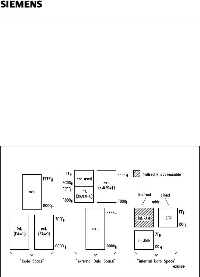
Memory Organisation
According to the SAB 8051 architecture, the SAB 80C515A has separate address spaces for program and data memory. Figure 2 illustrates the mapping of address spaces.
Figure 2
Memory Map
Semiconductor Group |
12 |

SAB 80C515A/83C515A-5
Program Memory ('Code Space')
The SAB 83C515A-5 has 32 Kbyte of on-chip ROM, while the SAB 80C515A has no internal
ROM. The program memory can externally be expanded up to 64 Kbyte. Pin EA determines whether program fetches below address 8000H are done from internal or external memory.
As a new feature the SAB 83C515A-5 offers the possibility of protecting the internal ROM against unauthorized access. This protection is implemented in the ROM-Mask. Therefore, the decision ROM-Protection 'yes' or 'no' has to be made when delivering the ROM-Code. Once enabled, there is no way of disabling the ROM-Protection.
Effect: |
The access to internal ROM done by an externally fetched MOVC instruction is |
|
disabled. Nevertheless, an access from internal ROM to external ROM is possible. |
To verify the read protected ROM-Code a special ROM-Verify-Mode is implemented. This mode also can be used to verify unprotected internal ROM.
ROM -Protection |
ROM-Verification Mode |
Restrictions |
|
|
(see 'AC Characteristics') |
|
|
|
|
|
|
no |
ROM-Verification Mode 1 |
– |
|
|
(standard 8051 Verification Mode) |
|
|
|
ROM-Verification Mode 2 |
|
|
|
|
|
|
yes |
ROM-Verification Mode 2 |
– |
standard 8051 |
|
|
|
Verification Mode is |
|
|
|
disabled |
|
|
– |
externally applied MOVC |
|
|
|
accessing internal ROM |
|
|
|
is disabled |
|
|
|
|
Semiconductor Group |
13 |

SAB 80C515A/83C515A-5
Data Memory ('Data Space')
The data memory space consists of an internal and an external memory space.The
SAB 80C515A contains another 1 Kbyte on On-Chip RAM additional to the 256-bytes internal
RAM of the base type SAB 80C515. This RAM is called XRAM ('extended RAM') in this document.
External Data Memory
Up to 64 Kbyte external data memory can be addressed by instructions that use 8-bit or 16-bit indirect addressing. For 8-bit addressing MOVX instructions in combination with registers R0 and R1 can be used. A 16-bit external memory addressing is supported by a 16-bit datapointer. Registers XPAGE and SYSCON are controlling whether data fetches at addresses F800H to FBFFH are done from internal XRAM or from external data memory.
Internal Data Memory
The internal data memory is divided into four physically distinct blocks:
–the lower 128 bytes of RAM including four register banks containing eight registers each
–the upper 128 byte of RAM
–the 128 byte special function register area.
–a 1 K × 8 area which is accessed like external RAM (MOVX-instructions), implemented on
chip at the address range from F800H to FBFFH. Special Function Register SYSCON controls whether data is read from or written to XRAM or external RAM.
A map of the internal data memory is shown in figure 2. The overlapping address spaces of the standard internal data memory (256 byte) are accessed by different addressing modes (see User's Manual SAB 80C515). The stack can be located anywhere in the internal data memory.
Architecture of the XRAM
The contents of the XRAM is not affected by a reset or HW Power Down. After power-up the contents is undefined, while it remains unchanged during and after a reset or HW Power Down if the power supply is not turned off.
The additional On-Chip RAM is logically located in the "external data memory" range at the upper end of the 64 Kbyte address range (F800H-FBFFH). Nevertheless when XRAM is enabled the address range F800H to FFFFH is occupied. This is done to assure software compatibility to SAB 80C517A. It is possible to enable and disable (only by reset) the XRAM. If it is disabled the device shows the same behaviour as the parts without XRAM, i.e. all MOVX accesses use the external bus to physically external data memory.
Semiconductor Group |
14 |

SAB 80C515A/83C515A-5
Accesses to XRAM
Because the XRAM is used in the same way as external data memory the same instruction types must be used for accessing the XRAM.
Note: If a reset occurs during a write operation to XRAM, the effect on XRAM depends on the cycle which the reset is detected at (MOVX is a 2-cycle instruction):
Reset detection at cycle 1: The new value will not be written to XRAM. The old value is not affected.
Reset detection at cycle 2: The old value in XRAM is overwritten by the new value.
Accesses to XRAM using the DPTR
There are a Read and a Write instruction from and to XRAM which use one of the 16-bit DPTR for indirect addressing. The instructions are:
MOVX A, |
@DPTR (Read) |
MOVX |
@DPTR, A (Write) |
Normally the use of these instructions would use a physically external memory. However, in the SAB 80C515A the XRAM is accessed if it is enabled and if the DPTR points to the XRAM address space (DPTR ≥ F800H).
Accesses to XRAM using the Registers R0/R1
The 8051 architecture provides also instructions for accesses to external data memory range which use only an 8-bit address (indirect addressing with registers R0 or R1). The instructions are:
MOVX A, |
@Ri (Read) |
MOVX |
@Ri, A (Write) |
In application systems, either a real 8-bit bus (with 8-bit address) is used or Port 2 serves as page register which selects pages of 256-byte. However, the distinction, whether Port 2 is used as general purpose I/O or as "page address" is made by the external system design. From the device’s point of view it cannot be decided whether the Port 2 data is used externally as address or as I/O data!
Hence, a special page register is implemented into the SAB 80C515A to provide the possibility of accessing the XRAM also with the MOVX @Ri instructions, i.e. XPAGE serves the same function for the XRAM as Port 2 for external data memory.
Semiconductor Group |
15 |

SAB 80C515A/83C515A-5
Special Function Register XPAGE
Addr. 91H |
|
|
|
|
|
|
|
|
XPAGE |
The reset value of XPAGE is 00H.
XPAGE can be set and read by software.
The register XPAGE provides the upper address byte for accesses to XRAM with MOVX @Ri instructions. If the address formed from XPAGE and Ri is less than the XRAM address range, then an external access is performed. For the SAB 80C515A the contents of XPAGE must be greater or equal than F8H in order to use the XRAM. Of course, the XRAM must be enabled if it shall be used with MOVX @Ri instructions.
Thus, the register XPAGE is used for addressing of the XRAM; additionally its contents are used for generating the internal XRAM select. If the contents of XPAGE is less than the XRAM address range then an external bus access is performed where the upper address byte is provided by P2 and not by XPAGE!
Therefore, the software has to distinguish two cases, if the MOVX @Ri instructions with paging shall be used:
a) Access to XRAM: |
The upper address byte must be written to XPAGE or P2; |
|
both writes selects the XRAM address range. |
b) Access to external memory: The upper address byte must be written to P2; XPAGE will be loaded with the same address in order to deselect the XRAM.
Semiconductor Group |
16 |

SAB 80C515A/83C515A-5
Control of XRAM in the SAB 80C515A
There are two control bits in register SYSCON which control the use and the bus operation during accesses to the additional On-Chip RAM (XRAM).
Special Function Register SYSCON
Addr. 0B1H |
|
|
|
|
|
|
|
|
|
|
|
|
|
|
|
XMAP1 |
XMAP0 |
SYSCON |
|
|
|
|
|
|
|||||||||||||
Bit |
|
Function |
||||||||||||||||
|
|
|
|
|
|
|||||||||||||
XMAP0 |
|
Global enable/disable bit for XRAM memory. |
||||||||||||||||
|
|
XMAP0 =0: The access to XRAM (= On-Chip XDATA memory) is en- |
||||||||||||||||
|
|
|
|
abled. |
||||||||||||||
|
|
XMAP0 = 1: The access to XRAM is disabled. All MOVX accesses are |
||||||||||||||||
|
|
|
|
performed by the external bus (reset state). |
||||||||||||||
|
|
|
|
|
|
|
|
|
|
|
|
|
|
|
|
|||
XMAP1 |
|
Control bit for / |
|
|
|
|
|
|
|
|
|
|
|
|
|
|
||
RD/WRsignals during accesses to XRAM; this bit has no |
||||||||||||||||||
|
|
effect if XRAM is disabled (XMAP0 = 1) or if addresses exceeding the |
||||||||||||||||
|
|
XRAM address range are used for MOVX accesses. |
||||||||||||||||
|
|
XMAP1 = 0: The signals |
RD |
|
and |
WR |
are not activated during accesses |
|||||||||||
|
|
|
|
to XRAM. |
||||||||||||||
|
|
XMAP1 = 1: The signals |
|
and |
|
are activated during accesses to |
||||||||||||
|
RD |
WR |
||||||||||||||||
|
|
|
|
XRAM. |
||||||||||||||
|
|
|
|
|
|
|
|
|
|
|
|
|
|
|
|
|
|
|
Reset value of SYSCON is XXXX XX01B.
The control bit XMAP0 is a global enable/disable bit for the additional On-Chip RAM (XRAM). If this bit is set, the XRAM is disabled, all MOVX accesses use external memory via the external bus. In this case the SAB 80C515A does not use the additional On-Chip RAM and is compatible with the types without XRAM.
Semiconductor Group |
17 |
 Loading...