


Microcomputer Components
8-Bit CMOS Microcontroller
C509-L
Data Sheet 09.96

C509-L
|
|
8-Bit CMOS Microcontroller |
C509-L |
Advance Information
•Full upward compatibility with SAB 80C517/80C517A and 8051/C501 microcontrollers
•256 byte on-chip RAM
•3K byte of on-chip XRAM
•256 directly addressable bits
•375 ns instruction cycle at 16-MHz oscillator frequency
•On-chip emulation support logic (Enhanced Hooks Technology TM)
•External program and data memory expandable up to 64 Kbyte each
•8-bit A/D converter with 15 multiplexed inputs and built-in self calibration
•Two 16-bit timers/counters (8051 compatible)
•Three 16-bit timers/counters (can be used in combination with the compare/capture unit)
•Powerful compare/capture unit (CCU) with up to 29 high-speed or PWM output channels or 13 capture inputs
•Arithmetic unit for division, multiplication, shift and normalize operations
•Eight datapointers instead of one for indirect addressing of program and external data memory
(further features are on next page)
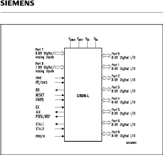
Figure 1
C509-L Functional Units
Semiconductor Group |
1 |
09.96 |

C509-L
Features (continued) :
•Extended watchdog facilities
–15-bit programmable watchdog timer
–Oscillator watchdog
•Ten I/O ports
–Eight bidirectional 8-bit I/O ports with selectable port structure quasi-bidirectional port structure (8051 compatible) bidirectional port structure with CMOS voltage levels
–One 8-bit and one 7-bit input port for analog and digital input signals
•Two full-duplex serial interfaces with own baud rate generators
•Four priority level interrupt systems, 19 interrupt vectors
•Three power saving modes
–Slow-down mode
–Idle mode
–Power-down mode
•Siemens high-performance ACMOS technology
•M-QFP-100-2 rectangular quad flat package
• Temperature Ranges : SAB-C509-L |
TA = 0 to 70 °C |
SAF-C509-L |
TA = -40 to 85 °C |
The C509-L is a high-end microcontroller in the Siemens C500 8-bit microcontroller family. lt is based on the well-known industry standard 8051 architecture; a great number of enhancements and new peripheral features extend its capabilities to meet the extensive requirements of new applications. Further, the C509-L is a superset of the Siemens SAB 80C517/80C517A 8-bit microcontroller thus offering an easy upgrade path for SAB 80C517/80C517A users.
The high performance of the C509-L microcontroller is achieved by the C500-Core with a maximum operating frequency of 16 MHz internal (and external) CPU clock. While maintaining all the features of the SAB 80C517A, the C509-L is expanded by one I/O port, in its compare/capture capabilities, by A/D converter functions, by additional 1 KByte of on-chip RAM (now 3 KByte XRAM) and by an additional user-selectable CMOS port structure. The C509-L is mounted in a P-MQFP-100-2 package.
Ordering Information
Type |
Ordering Code |
Package |
Description |
|
|
|
(8-Bit CMOS microcontroller) |
|
|
|
|
SAB-C509-LM |
Q67120-C1045 |
P-MQFP-100-2 |
for external memory (16 MHz) |
|
|
|
|
SAF-C509-LM |
Q67120-C0983 |
P-MQFP-100-2 |
for external memory (16 MHz) |
|
|
|
ext. temp. – 40 ˚C to 85 ˚C |
|
|
|
|
Note: Versions for extended temperature ranges – 40 ˚C to 110 ˚C (SAH-C509-L) and – 40 ˚C to 125 ˚C (SAK-C509-L) are available on request.
Semiconductor Group |
2 |
C509-L
Figure 2
Logic Symbol
Semiconductor Group |
3 |
09.96 |

C509-L |
Figure 3
C509-L Pin Configuration (P-MQFP-100-2, Top View)
Semiconductor Group |
4 |

C509-L
Table 1
Pin Definitions and Functions
Symbol |
Pin Number |
I/O*) |
Function |
|
|
|
|
|||
|
|
|
|
|
|
|
|
|
|
|
P1.0 - P1.7 |
9-6, 1, |
I/O |
Port 1 |
|
|
|
|
|
|
|
|
100-98 |
|
is an 8-bit quasi-bidirectional I/O port with internal pullup |
|||||||
|
|
|
resistors. Port 1 pins that have 1's written to them are |
|||||||
|
|
|
pulled high by the internal pullup resistors, and in that |
|||||||
|
|
|
state can be used as inputs. As inputs, port 1 pins being |
|||||||
|
|
|
externally pulled low will source current (I IL, in the DC |
|||||||
|
|
|
characteristics) because of the internal pullup resistors. |
|||||||
|
|
|
Port 1 can also be switched into a bidirectional mode, in |
|||||||
|
|
|
which CMOS levels are provided. In this bidirectional |
|||||||
|
|
|
mode, each port 1 pin can be programmed individually |
|||||||
|
|
|
as input or output. |
|
|
|
||||
|
|
|
Port 1 also contains the interrupt, timer, clock, capture |
|||||||
|
|
|
and compare pins that are used by various options. The |
|||||||
|
|
|
output latch corresponding to a secondary function must |
|||||||
|
|
|
be programmed to a one (1) for that function to operate |
|||||||
|
|
|
(except when used for the compare functions). |
|||||||
|
|
|
The secondary functions are assigned to the pins of |
|||||||
|
|
|
port 1 as follows : |
|
|
|
||||
|
9 |
|
P1.0 |
|
|
|
CC0 |
|
|
/ compare 0 output / |
|
|
INT3 |
Interrupt 3 input |
|||||||
|
|
|
|
|
|
|
|
capture 0 input |
||
|
8 |
|
P1.1 |
INT4 |
CC1 |
Interrupt 4 input / compare 1 output / |
||||
|
|
|
|
|
|
|
|
capture 1 input |
||
|
7 |
|
P1.2 |
INT5 |
CC2 |
Interrupt 5 input / compare 2 output / |
||||
|
|
|
|
|
|
|
|
capture 2 input |
||
|
6 |
|
P1.3 |
INT6 |
CC3 |
Interrupt 6 input / compare 3 output / |
||||
|
|
|
|
|
|
|
|
capture 3 input |
||
|
1 |
|
P1.4 |
|
|
CC4 |
|
input / compare 4 output / |
||
|
|
INT2 |
Interrupt 2 |
|||||||
|
|
|
|
|
|
|
|
capture 4 input |
||
|
100 |
|
P1.5 |
T2EX |
|
Timer 2 external reload trigger input |
||||
|
99 |
|
P1.6 |
CLKOUT |
System clock output |
|||||
|
98 |
|
P1.7 |
T2 |
|
Counter 2 input |
||||
|
|
|
|
|
|
|
|
|
|
|
*) I = Input O = Output
Semiconductor Group |
5 |
09.96 |

C509-L
Table 1
Pin Definitions and Functions (cont’d)
Symbol |
Pin Number |
I/O*) |
Function |
|
|
|
|
|
|
P9.0 - P9.7 |
74-77, |
I/O |
Port 9 |
|
|
5-2 |
|
is an 8-bit quasi-bidirectional I/O port with internal pullup |
|
|
|
|
resistors. Port 9 pins that have 1's written to them are |
|
|
|
|
pulled high by the internal pullup resistors, and in that |
|
|
|
|
state can be used as inputs. As inputs, port 9 pins being |
|
|
|
|
externally pulled low will source current (I IL, in the DC |
|
|
|
|
characteristics) because of the internal pullup resistors. |
|
|
|
|
Port 9 can also be switched into a bidirectional mode, in |
|
|
|
|
which CMOS levels are provided. In this bidirectional |
|
|
|
|
mode, each port 1 pin can be programmed individually |
|
|
|
|
as input or output. |
|
|
|
|
Port 9 also serves alternate compare functions. The out- |
|
|
|
|
put latch corresponding to a secondary function must be |
|
|
|
|
programmed to a one (1) for that function to operate. |
|
|
|
|
The secondary functions are assigned to the pins of |
|
|
|
|
port 9 as follows : |
|
|
|
|
P9.0-P9.7 CC10-CC17 Compare/capture channel 0-7 |
|
|
|
|
output/input |
|
|
|
|
|
|
XTAL2 |
12 |
– |
XTAL2 |
|
|
|
|
is the input to the inverting oscillator amplifier and input |
|
|
|
|
to the internal clock generator circuits. |
|
|
|
|
When supplying the C509-L with an external clock |
|
|
|
|
source, XTAL2 should be driven, while XTAL1 is left |
|
|
|
|
unconnected. A duty cycle of 0.4 to 0.6 of the clock |
|
|
|
|
signal is required. Minimum and maximum high and low |
|
|
|
|
times as well as rise/fall times specified in the AC |
|
|
|
|
characteristics must be observed. |
|
|
|
|
|
|
XTAL1 |
13 |
– |
XTAL1 |
|
|
|
|
Output of the inverting oscillator amplifier. This pin is |
|
|
|
|
used for the oscillator operation with crystal or ceramic |
|
|
|
|
resonartor |
|
|
|
|
|
|
*) I = Input |
|
|
|
|
O = Output |
|
|
|
|
Semiconductor Group |
6 |

C509-L
Table 1
Pin Definitions and Functions (cont’d)
Symbol |
Pin Number |
I/O*) |
|
Function |
|
|
|
|
|
|
|
|
|
|||||||
|
|
|
|
|
|
|
|
|
|
|
|
|
|
|||||||
P2.0 – P2.7 |
14-21 |
I/O |
|
Port 2 |
|
|
|
|
|
|
|
|
|
|||||||
|
|
|
|
|
|
|
|
is a 8-bit I/O port. Port 2 emits the high-order address |
||||||||||||
|
|
|
|
|
|
|
|
byte during fetches from external program memory and |
||||||||||||
|
|
|
|
|
|
|
|
during accesses to external data memory that use 16-bit |
||||||||||||
|
|
|
|
|
|
|
|
addresses (MOVX @DPTR). In this application it uses |
||||||||||||
|
|
|
|
|
|
|
|
strong internal pullup resistors when issuing 1s. During |
||||||||||||
|
|
|
|
|
|
|
|
accesses to external data memory that use 8-bit |
||||||||||||
|
|
|
|
|
|
|
|
addresses (MOVX @Ri), port 2 issues the contents of the |
||||||||||||
|
|
|
|
|
|
|
|
P2 special function register. |
|
|
|
|||||||||
|
|
|
|
|
|
|
|
P2.0 - P2.7 |
A8 - A15 |
Address lines 8 - 15 |
||||||||||
|
|
|
|
|
|
|
|
|
|
|
|
|
|
|
|
|
|
|
||
|
|
/ |
|
|
22 |
O |
|
|
|
|
|
|
|
|
/ |
|
|
|
|
|
PSEN |
RDF |
Program Store Enable |
Read FLASH |
|||||||||||||||||
|
|
|
|
|
|
|
|
The |
|
|
|
output is a control signal that enables the |
||||||||
|
|
|
|
|
|
|
|
PSEN |
||||||||||||
|
|
|
|
|
|
|
|
external program memory to the bus during external |
||||||||||||
|
|
|
|
|
|
|
|
code fetch operations. It is activated every third |
||||||||||||
|
|
|
|
|
|
|
|
oscillator period. |
|
is not activated during external |
||||||||||
|
|
|
|
|
|
|
|
PSEN |
||||||||||||
|
|
|
|
|
|
|
|
data memory accesses caused by MOVX instructions. |
||||||||||||
|
|
|
|
|
|
|
|
|
is not activated when instructions are executed |
|||||||||||
|
|
|
|
|
|
|
|
PSEN |
||||||||||||
|
|
|
|
|
|
|
|
from the internal Boot ROM or from the XRAM. |
||||||||||||
|
|
|
|
|
|
|
|
In external programming mode |
|
becomes active |
||||||||||
|
|
|
|
|
|
|
|
RDF |
||||||||||||
|
|
|
|
|
|
|
|
when executing external data memory read (MOVX) |
||||||||||||
|
|
|
|
|
|
|
|
instructions. |
|
|
|
|||||||||
|
|
|
|
|
|
|
|
|||||||||||||
ALE |
23 |
O |
|
Address Latch Enable |
|
|
|
|||||||||||||
|
|
|
|
|
|
|
|
This output is used for latching the low byte of the |
||||||||||||
|
|
|
|
|
|
|
|
address into external memory during normal operation. |
||||||||||||
|
|
|
|
|
|
|
|
It is activated every third oscillator period except during |
||||||||||||
|
|
|
|
|
|
|
|
an external data memory access caused by MOVX |
||||||||||||
|
|
|
|
|
|
|
|
instructions. |
|
|
|
|||||||||
|
|
|
|
|
|
|
|
|
|
|||||||||||
|
|
24 |
I |
|
|
|
|
|
|
|
|
|
|
|
|
|
||||
EA |
External Access Enable |
|
|
|
||||||||||||||||
|
|
|
|
|
|
|
|
The status of this pin is latched at the end of a reset. |
||||||||||||
|
|
|
|
|
|
|
|
When held at low level, the C509-L fetches all |
||||||||||||
|
|
|
|
|
|
|
|
instructions from the external program memory. For the |
||||||||||||
|
|
|
|
|
|
|
|
C509-L this pin must be tied low. |
||||||||||||
|
|
|
|
|
||||||||||||||||
PRGEN |
25 |
I |
|
External Flash-EPROM Program Enable |
||||||||||||||||
|
|
|
|
|
|
|
|
A low level at this pin disables the programming of an |
||||||||||||
|
|
|
|
|
|
|
|
external Flash-EPROM. To enable the programming of |
||||||||||||
|
|
|
|
|
|
|
|
an external Flash-EPROM, the pin PRGEN must be held |
||||||||||||
|
|
|
|
|
|
|
|
at high level and bit PRGEN1 in SFR SYSCON1 has to |
||||||||||||
|
|
|
|
|
|
|
|
be set. There is no internal pullup resistor connected to |
||||||||||||
|
|
|
|
|
|
|
|
this pin. |
|
|
|
|
|
|
|
|
|
|||
|
|
|
|
|
|
|
|
|
|
|
|
|
|
|
|
|
||||
*) I = Input |
|
|
|
|
|
|
|
|
|
|
|
|
|
|
|
|
||||
|
O = Output |
|
|
|
|
|
|
|
|
|
|
|
|
|
|
|
|
|||
Semiconductor Group |
7 |
09.96 |

C509-L
Table 1
Pin Definitions and Functions (cont’d)
Symbol |
Pin Number |
I/O*) |
|
Function |
|
||
|
|
|
|
|
|
||
P0.0 – P0.7 |
26, 27, |
I/O |
|
Port 0 |
|
||
|
|
30-35 |
|
|
is an 8-bit open-drain bidirectional I/O port. Port 0 pins |
||
|
|
|
|
|
that have 1s written to them float, and in that state can be |
||
|
|
|
|
|
used as high-impendance inputs. Port 0 is also the |
||
|
|
|
|
|
multiplexed low-order address and data bus during |
||
|
|
|
|
|
accesses to external program or data memory. In this |
||
|
|
|
|
|
operating mode it uses strong internal pullup resistors |
||
|
|
|
|
|
when issuing 1 s. |
|
|
|
|
|
|
|
P0.0 - P0.7 AD0-AD7 |
Address/data lines 0 - 7 |
|
|
|
|
|
|
|
|
|
|
|
36 |
I |
|
|
|
|
HWPD |
Hardware Power Down |
|
|||||
|
|
|
|
|
A low level on this pin for the duration of one machine |
||
|
|
|
|
|
cycle while the oscillator is running resets the C509-L. |
||
|
|
|
|
|
A low level for a longer period will force the part to power |
||
|
|
|
|
|
down mode with the pins floating. There is no internal |
||
|
|
|
|
|
pullup resistor connected to this pin. |
||
|
|
|
|
|
|
||
P5.0 - P5.7 |
44-37 |
I/O |
|
Port 5 |
|
||
|
|
|
|
|
is an 8-bit quasi-bidirectional I/O port with internal pullup |
||
|
|
|
|
|
resistors. Port 5 pins that have 1's written to them are |
||
|
|
|
|
|
pulled high by the internal pullup resistors, and in that |
||
|
|
|
|
|
state can be used as inputs. As inputs, port 5 pins being |
||
|
|
|
|
|
externally pulled low will source current (I IL, in the DC |
||
|
|
|
|
|
characteristics) because of the internal pullup resistors. |
||
|
|
|
|
|
Port 5 can also be switched into a bidirectional mode, in |
||
|
|
|
|
|
which CMOS levels are provided. In this bidirectional |
||
|
|
|
|
|
mode, each port 5 pin can be programmed individually |
||
|
|
|
|
|
as input or output. |
|
|
|
|
|
|
|
Port 5 also serves as alternate function for “Concurrent |
||
|
|
|
|
|
Compare” and "Set/Reset compare” functions. The |
||
|
|
|
|
|
output latch corresponding to a secondary function must |
||
|
|
|
|
|
be programmed to a one (1) for that function to operate. |
||
|
|
|
|
|
The secondary functions are assigned to the pins of port |
||
|
|
|
|
|
5 as follows : |
|
|
|
|
|
|
|
P5.0 - P5.7 CCM0-CCM7 |
Concurrent Compare |
|
|
|
|
|
|
|
|
or Set/Reset lines 0 - 7 |
|
|
|
|
|
|
|
|
*) I = Input |
|
|
|
|
|
|
|
O = Output |
|
|
|
|
|
|
|
Semiconductor Group |
8 |

C509-L
Table 1
Pin Definitions and Functions (cont’d)
Symbol |
Pin Number |
I/O*) |
Function |
|
|
|
|
|
||
|
|
|
|
|||||||
OWE |
45 |
I |
Oscillator Watchdog Enable |
|||||||
|
|
|
A high level on this pin enables the oscillator watchdog. |
|||||||
|
|
|
When left unconnected, this pin is pulled high by a weak |
|||||||
|
|
|
internal pullup resistor. The logic level at OWE should |
|||||||
|
|
|
not be changed during normal operation. When held at |
|||||||
|
|
|
low level the oscillator watchdog function is turned off. |
|||||||
|
|
|
During hardware power down the pullup resistor is |
|||||||
|
|
|
switched off. |
|
|
|
|
|
||
|
|
|
|
|
|
|
|
|
|
|
P6.0 - P6.7 |
46-50, |
I/O |
Port 6 |
|
|
|
|
|
|
|
|
54-56 |
|
is an 8-bit quasi-bidirectional I/O port with internal pullup |
|||||||
|
|
|
resistors. Port 6 pins that have 1's written to them are |
|||||||
|
|
|
pulled high by the internal pullup resistors, and in that |
|||||||
|
|
|
state can be used as inputs. As inputs, port 6 pins being |
|||||||
|
|
|
externally pulled low will source current (I IL, in the DC |
|||||||
|
|
|
characteristics) because of the internal pullup resistors. |
|||||||
|
|
|
Port 6 can also be switched into a bidirectional mode, in |
|||||||
|
|
|
which CMOS levels are provided. In this bidirectional |
|||||||
|
|
|
mode, each port 6 pin can be programmed individually |
|||||||
|
|
|
as input or output. |
|||||||
|
|
|
Port 6 also contains the external A/D converter control |
|||||||
|
|
|
pin, the receive and transmission lines for the serial port |
|||||||
|
|
|
1, and the write-FLASH control signal. The output latch |
|||||||
|
|
|
corresponding to a secondary function must be |
|||||||
|
|
|
programmed to a one (1) for that function to operate. |
|||||||
|
|
|
The secondary functions are assigned to the pins of |
|||||||
|
|
|
port 6 as follows : |
|||||||
|
46 |
|
P6.0 |
|
|
External A/D converter start pin |
||||
|
|
ADST |
||||||||
|
47 |
|
P6.1 |
R×D1 |
Receiver data input of serial interface 1 |
|||||
|
48 |
|
P6.2 |
T×D1 |
Transmitter data output of serial |
|||||
|
|
|
|
|
|
interface 1 |
||||
|
49 |
|
P6.3 |
|
|
The |
|
(write Flash) signal is active |
||
|
|
WRF |
WRF |
|||||||
|
|
|
|
|
|
when the programming mode is |
||||
|
|
|
|
|
|
selected. In this mode |
|
becomes |
||
|
|
|
|
|
|
WRF |
||||
|
|
|
|
|
|
active when executing external data |
||||
|
|
|
|
|
|
memory write (MOVX) instructions. |
||||
|
|
|
|
|
|
|
|
|
|
|
*) I = Input |
|
|
|
|
|
|
|
|
|
|
O = Output |
|
|
|
|
|
|
|
|
|
|
Semiconductor Group |
9 |
09.96 |
C509-L
Table 1
Pin Definitions and Functions (cont’d)
Symbol |
Pin Number |
I/O*) |
|
Function |
|
|
|
|
|||
|
|
|
|
|
|
|
|
|
|||
P8.0 - P8.6 |
57-60, |
I |
|
Port 8 |
|
|
|
|
|||
|
|
|
51-53 |
|
|
is a 7-bit unidirectional input port. Port pins can be used |
|||||
|
|
|
|
|
|
for digital input if voltage levels meet the specified input |
|||||
|
|
|
|
|
|
high/low voltages, and for the higher 7-bit of the |
|||||
|
|
|
|
|
|
multiplexed analog inputs of the A/D converter |
|||||
|
|
|
|
|
|
simultaneously. |
|
|
|
|
|
|
|
|
|
|
|
P8.0 - P8.6 |
AIN8 - AIN14 |
|
Analog input 8 - 14 |
||
|
|
|
|
|
|
|
|
|
|
|
|
|
|
|
61 |
O |
|
|
|
|
|
|
|
RO |
Reset Output |
|
|
|
|
||||||
|
|
|
|
|
|
This pin outputs the internally synchronized reset |
|||||
|
|
|
|
|
|
request signal. This signal may be generated by an |
|||||
|
|
|
|
|
|
external hardware reset, a watchdog timer reset or an |
|||||
|
|
|
|
|
|
oscillator watchdog reset. The |
|
output is active low. |
|||
|
|
|
|
|
|
RO |
|||||
|
|
|
|
|
|
|
|
|
|||
P4.0 – P4.7 |
64-66, |
I/O |
|
Port 4 |
|
|
|
|
|||
|
|
|
68-72 |
|
|
is an 8-bit quasi-bidirectional I/O port with internal pull-up |
|||||
|
|
|
|
|
|
resistors. Port 4 pins that have 1’s written to them are |
|||||
|
|
|
|
|
|
pulled high by the internal pull-up resistors, and in that |
|||||
|
|
|
|
|
|
state can be used as inputs. As inputs, port 4 pins being |
|||||
|
|
|
|
|
|
externally pulled low will source current (I IL, in the DC |
|||||
|
|
|
|
|
|
characteristics) because of the internal pull-up resistors. |
|||||
|
|
|
|
|
|
Port 4 also erves as alternate compare functions. The |
|||||
|
|
|
|
|
|
output latch corresponding to a secondary functionmust |
|||||
|
|
|
|
|
|
be programmed to a one (1) for that function to operate. |
|||||
|
|
|
|
|
|
The secondary functions are assigned to the pins of port |
|||||
|
|
|
|
|
|
4 as follows : |
|
|
|
|
|
|
|
|
|
|
|
P4.0 - P4.7 |
CM0 - CM7 |
Compare channel 0 - 7 |
|||
|
|
|
|
|
|
|
|||||
|
/ SWD |
67 |
I |
|
|
|
|
/ Start Watchdog Timer |
|||
PE |
Power Saving Modes Enable |
||||||||||
|
|
|
|
|
|
A low level on this pin allows the software to enter the |
|||||
|
|
|
|
|
|
power down mode, idle and slow down mode. If the low |
|||||
|
|
|
|
|
|
level is also seen during reset, the watchdog timer |
|||||
|
|
|
|
|
|
function is off on default. |
|
|
|||
|
|
|
|
|
|
Usage of the software controlled power saving modes is |
|||||
|
|
|
|
|
|
blocked, when this pin is held on high level. A high level |
|||||
|
|
|
|
|
|
during reset performs an automatic start of the watchdog |
|||||
|
|
|
|
|
|
timer immediately after reset. |
|
|
|||
|
|
|
|
|
|
When left unconnected this pin is pulled high by a weak |
|||||
|
|
|
|
|
|
internal pullup resistor. During hardware power down the |
|||||
|
|
|
|
|
|
pullup resistor is switched off. |
|
|
|||
|
|
|
|
|
|
|
|
|
|
||
*) I = Input |
|
|
|
|
|
|
|
|
|
||
|
|
O = Output |
|
|
|
|
|
|
|
|
|
Semiconductor Group |
10 |

C509-L
Table 1
Pin Definitions and Functions (cont’d)
Symbol |
Pin Number |
I/O*) |
|
Function |
|
|
||
|
|
|
|
|
|
|
|
|
|
|
73 |
I |
|
|
|
|
|
RESET |
RESET |
|
|
|||||
|
|
|
|
|
A low level on this pin for the duration of one machine |
|||
|
|
|
|
|
cycle while the oscillator is running resets the C509-L. A |
|||
|
|
|
|
|
small internal pullup resistor permits power-on reset |
|||
|
|
|
|
|
using only a capacitor connected to VSS. |
|||
|
|
|
|
|
||||
VAREF |
78 |
– |
|
Reference voltage for the A/D converter |
||||
VAGND |
79 |
– |
|
Reference ground for the A/D converter |
||||
P7.0 - P7.7 |
87-80 |
I |
|
Port 7 |
|
|
||
|
|
|
|
|
Port 7 is an 8-bit unidirectional input port. Port pins can |
|||
|
|
|
|
|
be used for digital input if voltage levels meet the |
|||
|
|
|
|
|
specified input high/low voltages, and for the lower 8-bit |
|||
|
|
|
|
|
of the multiplexed analog inputs of the A/D converter |
|||
|
|
|
|
|
simultaneously. |
|
|
|
|
|
|
|
|
P7.0 - P7.7 |
AIN0 - AIN7 |
Analog input 0 - 7 |
|
|
|
|
|
|
|
|
|
|
*) I = Input O = Output
Semiconductor Group |
11 |
09.96 |

C509-L
Table 1
Pin Definitions and Functions (cont’d)
Symbol |
Pin Number |
I/O*) |
Function |
|
|
|
||||||
|
|
|
|
|
|
|
|
|
|
|
|
|
P3.0 – P3.7 |
90-97 |
I/O |
Port 3 |
|
|
|
|
|
|
|
|
|
|
|
|
is an 8-bit quasi-bidirectional I/O port with internal pullup |
|||||||||
|
|
|
resistors. Port 3 pins that have 1's written to them are |
|||||||||
|
|
|
pulled high by the internal pullup resistors, and in that |
|||||||||
|
|
|
state can be used as inputs. As inputs, port 3 pins being |
|||||||||
|
|
|
externally pulled low will source current (I IL, in the DC |
|||||||||
|
|
|
characteristics) because of the internal pullup resistors. |
|||||||||
|
|
|
Port 3 also contains two external interrupt inputs, the |
|||||||||
|
|
|
timer 0/1 inputs, the serial port 0 receive/transmit line |
|||||||||
|
|
|
and the external memory strobe pins. The output latch |
|||||||||
|
|
|
corresponding to a secondary function must be |
|||||||||
|
|
|
programmed to a one (1) for that function to operate. |
|||||||||
|
|
|
The secondary functions are assigned to the port pins of |
|||||||||
|
|
|
port 3 as follows |
|||||||||
|
90 |
|
P3.0 |
R×D0 |
Receiver data input (asynchronous) or |
|||||||
|
|
|
|
|
|
|
|
|
|
data input/output (synchronous) of serial |
||
|
|
|
|
|
|
|
|
|
|
interface 0 |
||
|
91 |
|
P3.1 |
T×D0 |
Transmitter data output (asynchronous) |
|||||||
|
|
|
|
|
|
|
|
|
|
or clock output (synchronous) of the |
||
|
|
|
|
|
|
|
|
|
|
serial interface 0 |
||
|
92 |
|
P3.2 |
|
|
|
|
|
|
|
|
/ timer 0 gate control |
|
|
INT0 |
Interrupt 0 input |
|||||||||
|
93 |
|
P3.3 |
|
|
|
|
|
|
|
/ timer 1 gate control |
|
|
|
INT1 |
Interrupt 1 input |
|||||||||
|
94 |
|
P3.4 |
T0 |
Counter 0 input |
|||||||
|
95 |
|
P3.5 |
T1 |
Counter 1 input |
|||||||
|
96 |
|
P3.6 |
|
|
|
|
The write control signal latches the data |
||||
|
|
WR |
||||||||||
|
|
|
|
|
|
|
|
|
|
byte from port 0 into the external data |
||
|
|
|
|
|
|
|
|
|
|
memory |
||
|
97 |
|
P3.7 |
|
/ |
|
The read control signal enables the |
|||||
|
|
RD |
||||||||||
|
|
|
|
|
|
|
|
|
|
external data memory to port 0 |
||
|
|
|
|
|
|
|
(external program store enable) |
|||||
|
|
|
|
PSENX |
PSENX |
|||||||
|
|
|
|
|
|
|
|
|
|
enables the external code memory |
||
|
|
|
|
|
|
|
|
|
|
when the external / internal XRAM |
||
|
|
|
|
|
|
|
|
|
|
mode or external / internal programming |
||
|
|
|
|
|
|
|
|
|
|
mode is selected. |
||
|
|
|
|
|||||||||
VSS |
10, 28, 62, 88 |
– |
Circuit ground potential |
|||||||||
VCC |
11, 29, 63, 89 |
– |
Supply terminal for all operating modes |
|||||||||
*) I = Input |
|
|
|
|
|
|
|
|
|
|
|
|
O = Output |
|
|
|
|
|
|
|
|
|
|
|
|
Semiconductor Group |
12 |

C509-L |
Figure 4
Block Diagram of the C509-L
Semiconductor Group |
13 |
09.96 |

C509-L
CPU
The C509-L is efficient both as a controller and as an arithmetic processor. It has extensive facilities for binary and BCD arithmetic and excels in its bit-handling capabilities. Efficient use of program memory results from an instruction set consisting of 44 % one-byte, 41 % two-byte, and 15% threebyte instructions. With a 6 MHz crystal, 58% of the instructions are executed in 1.0 s (12 MHz: 500 ns, 16 MHz : 375 ns).
Special Function Register PSW (Address D0H) |
|
|
Reset Value : 00H |
||||||
Bit No. |
MSB |
|
|
|
|
|
|
LSB |
|
|
D7H |
D6H |
D5H |
D4H |
D3H |
D2H |
D1H |
D0H |
|
D0H |
CY |
AC |
F0 |
RS1 |
RS0 |
OV |
F1 |
P |
PSW |
Bit |
Function |
CY |
Carry Flag |
|
Used by arithmetic instruction. |
|
|
AC |
Auxiliary Carry Flag |
|
Used by instructions which execute BCD operations. |
|
|
F0 |
General Purpose Flag |
|
|
RS1 |
Register Bank select control bits |
RS0 |
These bits are used to select one of the four register banks. |
|
|
|
|
|
|
|
|
|
RS1 |
RS0 |
Function |
|
|
|
|
|
|
|
|
|
|
|
0 |
0 |
Bank 0 selected, data address 00H-07H |
|
|
|
|
0 |
1 |
Bank 1 selected, data address 08H-0FH |
|
|
|
|
1 |
0 |
Bank 2 selected, data address 10H-17H |
|
|
|
|
1 |
1 |
Bank 3 selected, data address 18H-1FH |
|
|
|
|
|
|
|
|
|
|
|
|
|
|
|
|
OV |
Overflow Flag |
|
|
|
||
|
Used by arithmetic instruction. |
|||||
|
|
|
|
|
|
|
F1 |
General Purpose Flag |
|
|
|
||
|
|
|
|
|
|
|
P |
Parity Flag |
|
|
|
|
|
|
Set/cleared by hardware after each instruction to indicate an odd/even |
|||||
|
number of "one" bits in the accumulator, i.e. even parity. |
|||||
Semiconductor Group |
14 |
C509-L
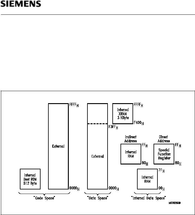
Memory Organization
The C509-L CPU manipulates data and operands in the following five address spaces:
–up to 64 Kbyte of external program memory
–up to 64 Kbyte of external data memory
–512 byte of internal Boot ROM (program memory)
–256 bytes of internal data memory
–3 Kbyte of external XRAM data memory
–a 128 byte special function register area
Figure 5 illustrates the memory address spaces of the C509-L.
Figure 5 |
C509-L Memory Map |
The C509-L can operate in four different operating modes (chipmodes) with different program and data memory organizations :
–Normal Mode
–XRAM Mode
–Bootstrap Mode
–Programming Mode
Table 2 describes the program and data memory areas which are available in the different chipmodes of the C509-L. It also shows the control bits of SFR SYSCON1, which are used for the software selection of the chipmodes. Figures 6 to 9 shows the four chipmode configurations with the code and data memory partitioning.
Semiconductor Group |
15 |
09.96 |

C509-L
Table 2
Overview of Program and Data Memory Organization
Operating Mode |
Program Memory |
Data Memory |
SYSCON1 Bits |
||||
(Chipmode) |
|
|
|
|
|
|
|
Ext. |
Int. |
Ext. |
Int. |
PRGEN |
SWAP |
||
|
|||||||
|
|
|
|
|
1 |
|
|
|
|
|
|
|
|
|
|
Normal Mode |
0000H - |
– |
0000H - |
F400H - |
0 |
0 |
|
|
FFFFH |
|
F3FFH |
FFFFH |
|
|
|
|
|
|
|
(XRAM) |
|
|
|
|
|
|
|
|
|
|
|
XRAM Mode |
0200H - |
0000H - |
0000H - |
– |
0 |
1 |
|
|
F3FFH |
01FFH = |
FFFFH |
|
|
|
|
|
|
Boot ROM; |
(read only) |
|
|
|
|
|
|
F400H - |
|
|
|
|
|
|
|
FFFFH = |
|
|
|
|
|
|
|
(XRAM) |
|
|
|
|
|
|
|
|
|
|
|
|
|
Bootstrap Mode |
0200H - |
0000H - |
0000H - |
F400H – |
1 |
0 |
|
|
F3FFH |
01FFH = |
F3FFH |
FFFFH |
|
|
|
|
|
Boot ROM |
|
(XRAM) |
|
|
|
|
|
|
|
|
|
|
|
Programming Mode |
0200H - |
0000H - |
0000H - |
– |
1 |
1 |
|
|
FFFFH |
01FFH = |
FFFFH |
|
|
|
|
|
|
Boot ROM; |
(read and |
|
|
|
|
|
|
F400H - |
write) |
|
|
|
|
|
|
FFFFH = |
|
|
|
|
|
|
|
XRAM |
|
|
|
|
|
|
|
|
|
|
|
|
|
Semiconductor Group |
16 |

C509-L
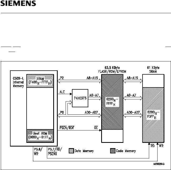
Normal Mode Configuration
The Normal Mode is the standard 8051 compatible operating mode of the C509-L. In this mode 64K byte external code memory and 61K byte external SRAM as well as 3K byte internal data memory (XRAM) are provided. If the is disabled (default after reset), totally 64K byte external data memory are available. The Boot ROM is disabled. The external program memory is controlled by the PSEN/ RDF signal. Read and write accesses to the external data memory are controlled by the RD and WR pins of port 3.
Figure 6
Locations of Codeand Data Memory in Normal Mode
Semiconductor Group |
17 |
09.96 |

C509-L
XRAM Mode Configuration
The XRAM Mode is implemented in the C509-L for executing e.g. up to 3K byte diagnostic software which has been loaded into the XRAM in the Bootstrap Mode via the serial interface. In this operating mode the Boot ROM, the XRAM, and the external data memory are mapped into the code memory area, while the external ROM/EPROM is mapped into the external data memory area. External program memory fetches from the SRAM are controlled by the P3.7/RD/PSENX pin. External data memory read accesses from the ROM/EPROM are controlled by the PSEN/RDF pin. In XRAM mode, the external data memory can only be read but not written.
Figure 7
Locations of Codeand Data Memory in XRAM Mode
Semiconductor Group |
18 |
C509-L
Bootstrap Mode Configuration
In the Bootstrap Mode the Boot ROM and the external FLASH/ROM/EPROM are mapped into the code memory area. 61K byte external SRAM as well as 3K byte internal data memory (XRAM) are provided in the external data memory area. The external program memory is controlled by the PSEN/RDF signal. Read and write accesses to the external data memory are controlled by the RD and WR pins of port 3.
Figure 8
Locations of Codeand Data Memory in Bootstrap Mode
Semiconductor Group |
19 |
09.96 |
C509-L
Programming Mode Configuration
The External Programming Mode is implemented for the in-circuit programming of external 5V-only FLASH EPROMs. Similar as in the XRAM mode, the Boot ROM, the XRAM, and the external data memory (SRAM) are mapped into the code memory area, while the external FLASH memory is mapped into the external data memory area. Additionally to the XRAM mode, the FLASH memory can also be written through external data memory accesses (MOVX instructions). External program memory fetches from the SRAM are controlled by the P3.7/RD/PSENX pin. External data memory read/write accesses from/to the ROM/EPROM are controlled by the PSEN/RDF and P6.3/WRF pin.
Figure 9
Locations of Codeand Data Memory in Programming Mode
Semiconductor Group |
20 |

C509-L
The Bootstrap Loader
The C509-L includes a bootstrap mode, which is activated by setting the PRGEN pin at logic high level at the rising edge of the RESET or the HWPD signal (bit PRGEN1=1). In this mode software routines of the bootstrap loader, located at the addresses 0000H to 01FFH in the boot ROM will be executed. Its purpose is to allow the easy and quick programming of the internal XRAM (F400H to FFFFH) via serial interface while the MCU is in-circuit. This allows to transfer custom routines to the XRAM, which will program an external 64 KByte FLASH memory. The serial routines of the bootstrap loader may be replaced by own custom software or even can be blocked to prevent unauthorized persons from reading out or writing to the external FLASH memory. Therefore the bootstrap loader checks an external FLASH memory for existing custom software and executes it.
The bootstrap loader consists of three functional parts which represent the three phases as described below.
Phase I : Check for existing custom software in the external FLASH memory and execute it.
Phase II : Establish a serial connection and automatically synchronize to the transfer speed (baud rate) of the serial communication partner (host).
Phase III : Perform the serial communication to the host. The host controls the bootstrap loader by sending header informations, which select one of four operating modes. These modes are :
Mode 0 : Transfer a custom program from the host to the XRAM (F400H - FFFFH). This mode returns to the beginning of phase III.
Mode 1 : Execute a custom program in the XRAM at any start address from F400H to FFFFH.
Mode 2 : Check the contents of any area of the external FLASH memory by calculating a checksum. This mode returns to the beginning of phase III.
Mode 3 : Execute a custom program in the FLASH memory at any start address beyond 0200H (at addresses 0000H to 01FFH the boot-ROM is active).
The three phases of the bootstrap loader program and their connections are illustrated in figure 10.
Semiconductor Group |
21 |
09.96 |

C509-L |
Figure 10
The Three Phases of the Bootstrap Loader
The serial communication, which is activated in phase II is performed with the integrated serial interface 0 of the C509-L. Using a fullor half-duplex serial cable (RS232) the MCU must be connected to the serial port of the host computer as shown in figure .
Figure 11
Bootstrap Loader Interface to the PC
Semiconductor Group |
22 |
 Loading...