


SAB-C515-1R24M
Siemens SAB-C515-1R24M, SAB-C515-1RM, SAB-C515-L24M, SAB-C515-LM, SAF-C515-1R24M Datasheet
...
Data Sheet 08.97
Microcomputer Components
C515
8-Bit CMOS Microcontroller

Edition 1997-08-01
Published by
Siemens AG,
Bereich Halbleiter, Marketing-
Kommunikation, Balanstraße 73,
81541 München
©
Siemens AG 1997.
All Rights Reserved.
Attention please!
As far as patents or other rights of third parties are concerned, liability is only assumed for components, not for applications, processes
and circuits implemented within components or assemblies.
The information describes the type of component and shall not be considered as assured characteristics.
Terms of delivery and rights to change design reserved.
For questions on technology, delivery and prices please contact the Semiconductor Group Offices in Germany or the Siemens Companies
and Representatives worldwide (see address list).
Due to technical requirements components may contain dangerous substances. For information on the types in question please contact
your nearest Siemens Office, Semiconductor Group.
Siemens AG is an approved CECC manufacturer.
Packing
Please use the recycling operators known to you. We can also help you – get in touch with your nearest sales office. By agreement we
will take packing material back, if it is sorted. You must bear the costs of transport.
For packing material that is returned to us unsorted or which we are not obliged to accept, we shall have to invoice you for any costs in-
curred.
Components used in life-support devices or systems must be expressly authorized for such purpose!
Critical components
1
of the Semiconductor Group of Siemens AG, may only be used in life-support devices or systems
2
with the express
written approval of the Semiconductor Group of Siemens AG.
1 A critical component is a component used in a life-support device or system whose failure can reasonably be expected to cause the
failure of that life-support device or system, or to affect its safety or effectiveness of that device or system.
2 Life support devices or systems are intended (a) to be implanted in the human body, or (b) to support and/or maintain and sustain hu-
man life. If they fail, it is reasonable to assume that the health of the user may be endangered.
C515 Data Sheet
Revision History: Current Version: 1997-08-01
Previous Version: none (Original Version)
Page
(in previous
Version)
Page
(in current
Version)
Subjects (major changes since last revision)
C515
Semiconductor Group 3 1997-08-01
Data Sheet
8-Bit CMOS Microcontroller
Advance Information
•
Full upward compatibility with SAB 80C515
•
Up to 24 MHz external operating frequency
– 500ns instruction cycle at 24 MHz operation
•
8K byte on-chip ROM (with optional ROM protection)
– alternatively up to 64K byte external program memory
•
Up to 64K byte external data memory
•
256 byte on-chip RAM
•
Six 8-bit parallel I/O ports
•
One input port for analog/digital input
•
Full duplex serial interface (USART)
– 4 operating modes, fixed or variable baud rates
•
Three 16-bit timer/counters
– Timer 0 / 1 (C501 compatible)
– Timer 2 for 16-bit reload, compare, or capture functions
(more features on next page)
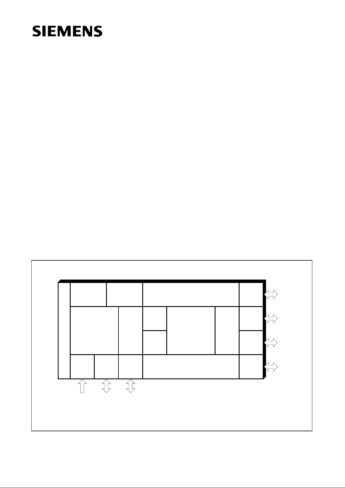
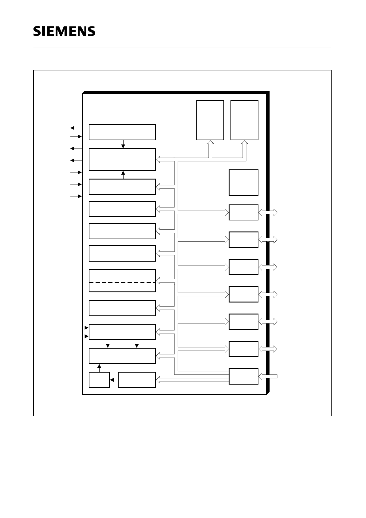
Figure 1
C515 Functional Units
MCA03198
On-Chip Emulation Support Module
Port 0
Port 1
Port 2
Port 3
RAM
256 x 8
CPU
T0
T1
USART
ROM
I/O
I/O
I/O
I/O
Port6Port 5 Port 4
Watchdog
Timer
A/D
Converter
I/O I/OAnalog/
Digital
Input
8-Bit
K8x8
Power
Modes
Saving
T2

C515
Semiconductor Group 4 1997-08-01
Features (cont’d):
•
8-bit A/D converter
– 8 multiplexed analog inputs
– Programmable reference voltages
•
16-bit watchdog timer
•
Power saving modes
– Idle mode
– Slow down mode (can be combined with idle mode)
– Software power-down mode
•
12 interrupt sources (7 external, 5 internal) selectable at four priority levels
•
On-chip emulation support logic (Enhanced Hooks Technology
TM
)
•
ALE switch-off capability
•
P-MQFP-80-1 package
•
Temperature Ranges : SAB-C515
T
A
= 0 to 70
°
C
SAF-C515
T
A
= -40 to 85
°
C
SAH-C515
T
A
= -40 to 110
°
C (max. operating frequency: 16 MHz)
The C515 is an upward compatible version of the SAB 80C515A 8-bit microcontroller which
additionally provides ALE switch-off capability, on-chip emulation support, ROM protection, and
slow down mode capability. With a maximum external clock rate of 24 MHz it achieves a 500 ns
instruction cycle time (1
µ
s at 12 MHz). The C515 is mounted in a P-MQFP-80 package.
Note:
Versions for extended temperature ranges – 40
˚C to 110
˚C (SAH-C515C-LM and SAH-
C515-1RM) are available on request. The ordering number of ROM types (DXXXX
extensions) is defined after program release (verification) of the customer.
Ordering Information
Type Ordering Code Package Description
(8-Bit CMOS microcontroller)
SAB-C515-1RM
SAB-C515-1R24M
Q67127-DXXXX
Q67127-DXXXX
P-MQFP-80-1
P-MQFP-80-1
with mask programmable ROM (16 MHz)
with mask programmable ROM (24 MHz)
SAF-C515-1RM Q67127-DXXXX P-MQFP-80-1 with mask programmable ROM (16 MHz)
ext. temp. – 40
˚C to 85
˚C
SAF-C515-1R24M Q67127-DXXXX P-MQFP-80-1 with mask programmable ROM (24 MHz)
ext. temp. – 40
˚C to 85
˚C
SAB-C515-LM
SAB-C515-L24M
Q67127-C1030
Q67127-C1032
P-MQFP-80-1
P-MQFP-80-1
for external memory (16 MHz)
for external memory (24 MHz
SAF-C515-LM Q67127-C1031 P-MQFP-80-1 for external memory (16 MHz)
ext. temp. – 40
˚C to 85
˚C
SAF-C515-L24M Q67127-C1081 P-MQFP-80-1 for external memory (24 MHz)
ext. temp. – 40
˚C to 85
˚C
Semiconductor Group 5 1997-08-01
C515
Figure 2
Logic Symbol
Additional Literature
For further information about the C515 the following literature is available:
Title Ordering Number
C515 8-Bit CMOS Microcontroller User’s Manual B158-H7049-X-X-7600
C500 Microcontroller Family
Architecture and Instruction Set User’s Manual
B158-H6987-X-X-7600
C500 Microcontroller Family - Pocket Guide B158-H6986-X-X-7600
MCL03199
XTAL1
XTAL2
RESET
EA
ALE
PSEN
C515
Port 0
8 Bit Digital I/O
1Port
Port 2
Port 3
V
SSCC
V
Digital Input
6Port
Port 5
4Port
PE
8 Bit Digital I/O
8 Bit Digital I/O
8 Bit Digital I/O
8 Bit Digital I/O
8 Bit Digital I/O
8 Bit Analog/
AREF
V
V
AGND
C515
Semiconductor Group 6 1997-08-01
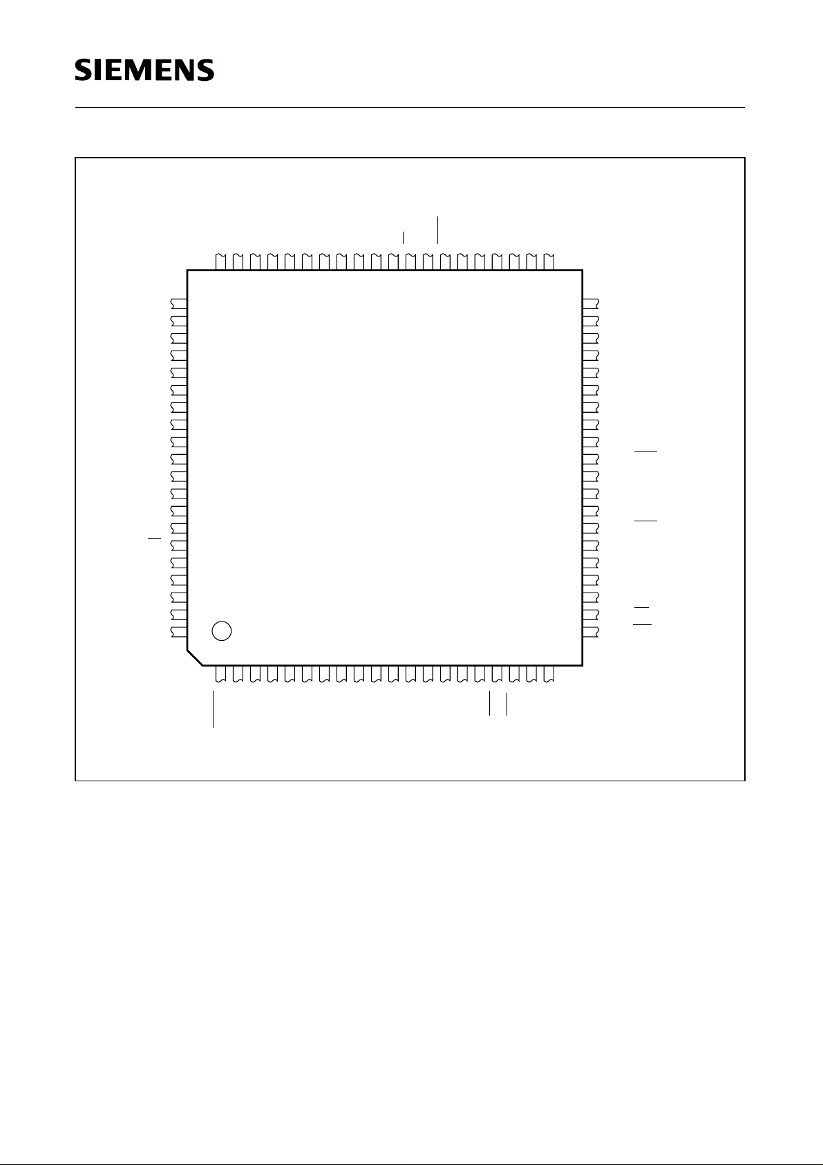
Figure 3
C515 Pin Configuration (P-MQFP-80 Package, Top View)
MCP03200
12
N.C.
345
P6.7/AIN7
6
P6.6/AIN6
7
P6.5/AIN5
8
P6.4/AIN4
9
P6.3/AIN3
10
P6.2/AIN2
11
P6.1/AIN1
12
P6.0/AIN0
13 14 15
P3.0/RXD
16
P3.1/TXD
17
P3.2/INT0
18
P3.3/INT1
19
P3.4/T0
20
P3.5/T1
V
AGND
4142434445464748495051525354555657585960
P0.7/AD7
P0.6/AD6
P0.5/AD5
P0.4/AD4
P0.3/AD3
P0.2/AD2
P0.1/AD1
P0.0/AD0
EA
ALE
PSEN
P2.7/A15
P2.6/A14
P2.5/A13
P2.4/A12
P2.3/A11
P4.7
P4.6
P4.5
P4.4
P4.3
PE
P4.2
P4.1
P4.0
N.C.
P5.0
P5.1
P5.2
P5.3
P5.4
P5.5
P3.6/WR
P3.7/RD
P1.7/T2
P1.6/CLKOUT
P1.5/T2EX
P1.4/INT2
P1.3/INT6/CC3
P1.2/INT5/CC2
P1.1/INT4/CC1
P1.0/INT3/CC0
XTAL2
XTAL1
P2.0/A8
P2.1/A9
62
63
64
65
66
67
68
69
70
71
72
73
74
75
76
77
78
79
80
39
38
37
36
35
34
33
32
31
30
29
28
27
26
25
24
23
22
21
4061
P5.6
P5.7
SS
V
CC
V
P2.2/A10
AREF
V
RESET
C515
N.C.
V
CC
N.C.
N.C.
N.C.
N.C.
N.C.
N.C.
N.C.
N.C.
N.C.
Semiconductor Group 7 1997-08-01
C515
Table 1
Pin Definitions and Functions
Symbol Pin Number
(P-MQFP-80)
I/O*) Function
RESET
1I
RESET
A low level on this pin for the duration of two machine
cycles while the oscillator is running resets the C515. A
small internal pullup resistor permits power-on reset
using only a capacitor connected to V
SS
.
VAREF 3 –
Reference voltage
for the A/D converter
VAGND 4 –
Reference ground
for the A/D converter
P6.0-P6.7 12-5 I
Port 6
is an 8-bit unidirectional input port to the A/D converter.
Port pins can be used for digital input, if voltage levels
simultaneously meet the specifications for high/low input
voltages and for the eight multiplexed analog inputs.
*) I = Input
O = Output

C515
Semiconductor Group 8 1997-08-01
P3.0-P3.7 15-22
15
16
17
18
19
20
21
22
I/O
Port 3
is an 8-bit quasi-bidirectional I/O port with internal pullup
resistors. Port 3 pins that have 1's written to them are
pulled high by the internal pullup resistors, and in that
state can be used as inputs. As inputs, port 3 pins being
externally pulled low will source current (
I
IL
, in the DC
characteristics) because of the internal pullup resistors.
Port 3 also contains the interrupt, timer, serial port and
external memory strobe pins that are used by various
options. The output latch corresponding to a secondary
function must be programmed to a one (1) for that
function to operate. The secondary functions are
assigned to the pins of port 3 as follows:
P3.0 / RxD Receiver data input (asynch.) or data
input/output (synch.) of serial interface
P3.1 / TxD Transmitter data output (asynch.) or
clock output (synch.) of serial interface
P3.2 / INT0
External interrupt 0 input /
timer 0 gate control input
P3.3 / INT1 External interrupt 1 input /
timer 1 gate control input
P3.4 / T0 Timer 0 counter input
P3.5 / T1 Timer 1 counter input
P3.6 / WR
WR control output; latches the data byte
from port 0 into the external data
memory
P3.7 / RD RD control output; enables the
external data memory
*) I = Input
O = Output
Table 1
Pin Definitions and Functions (cont’d)
Symbol Pin Number
(P-MQFP-80)
I/O*) Function
Semiconductor Group 9 1997-08-01
C515
P1.0 - P1.7 31-24
31
30
29
28
27
26
25
24
I/O
Port 1
is an 8-bit quasi-bidirectional I/O port with internal pullup
resistors. Port 1 pins that have 1's written to them are
pulled high by the internal pullup resistors, and in that
state can be used as inputs. As inputs, port 1 pins being
externally pulled low will source current (
I
IL
, in the DC
characteristics) because of the internal pullup resistors.
The port is used for the low-order address byte during
program verification. Port 1 also contains the interrupt,
timer, clock, capture and compare pins that are used by
various options. The output latch corresponding to a
secondary function must be programmed to a one (1) for
that function to operate (except when used for the
compare functions). The secondary functions are
assigned to the port 1 pins as follows :
P1.0 / INT3 /
CC0 Interrupt 3 input /
compare 0 output /
capture 0 input
P1.1 / INT4 /CC1 Interrupt 4 input /
compare 1 output /
capture 1 input
P1.2 / INT5 /CC2 Interrupt 5 input /
compare 2 output /
capture 2 input
P1.3 / INT6 /CC3 Interrupt 6 input /
compare 3 output /
capture 3 input
P1.4 / INT2
Interrupt 2 input
P1.5 / T2EX Timer 2 external reload /
trigger input
P1.6 / CLKOUT System clock output
P1.7 / T2 Counter 2 input
V
SS
34 –
Ground (0 V)
V
CC
33, 69 –
Supply voltage
during normal, idle, and power-down operation.
*) I = Input
O = Output
Table 1
Pin Definitions and Functions (cont’d)
Symbol Pin Number
(P-MQFP-80)
I/O*) Function
C515
Semiconductor Group 10 1997-08-01
XTAL2 36 –
XTAL2
Input to the inverting oscillator amplifier and input to the
internal clock generator circuits.
To drive the device from an external clock source,
XTAL2 should be driven, while XTAL1 is left
unconnected.
Minimum and maximum high and low
times as well as rise/fall times specified in the AC
characteristics must be observed.
XTAL1 37 – XTAL1
Output of the inverting oscillator amplifier.
P2.0-P2.7 38-45 I/O Port 2
is an 8-bit quasi-bidirectional I/O port with internal pullup
resistors. Port 2 pins that have 1's written to them are
pulled high by the internal pullup resistors, and in that
state can be used as inputs. As inputs, port 2 pins being
externally pulled low will source current (I
IL
, in the DC
characteristics) because of the internal pullup resistors.
Port 2 emits the high-order address byte during fetches
from external program memory and during accesses to
external data memory that use 16-bit addresses
(MOVX @DPTR). In this application it uses strong
internal pullup resistors when issuing 1's. During
accesses to external data memory that use 8-bit
addresses (MOVX @Ri), port 2 issues the contents of
the P2 special function register.
PSEN
47 O The Program Store Enable
output is a control signal that enables the external
program memory to the bus during external fetch
operations. It is activated every six oscillator periods,
except during external data memory accesses. The
signal remains high during internal program execution.
ALE 48 O The Address Latch enable
output is used for latching the address into external
memory during normal operation. It is activated every six
oscillator periods, except during an external data
memory access.
*) I = Input
O = Output
Table 1
Pin Definitions and Functions (cont’d)
Symbol Pin Number
(P-MQFP-80)
I/O*) Function
Semiconductor Group 11 1997-08-01
C515
EA 49 I External Access Enable
When held high, the C515 executes instructions from
the internal ROM (C515-1R) as long as the program
counter is less than 2000
H
. When held low, the C515
fetches all instructions from ext. program memory. For
the C515-L this pin must be tied low.
P0.0-P0.7 52-59 I/O Port 0
is an 8-bit open-drain bidirectional I/O port. Port 0 pins
that have 1's written to them float, and in that state can
be used as high-impedance inputs. Port 0 is also the
multiplexed low-order address and data bus during
accesses to external program and data memory. In this
application it uses strong internal pullup resistors when
issuing 1's. Port 0 also outputs the code bytes during
program verification in the C515-1R. External pullup
resistors are required during program verification.
P5.ß-P5.7 67-60 I/O Port 5
is an 8-bit quasi-bidirectional I/O port with internal pullup
resistors. Port 5 pins that have 1's written to them are
pulled high by the internal pullup resistors, and in that
state can be used as inputs. As inputs, port 5 pins being
externally pulled low will source current (I
IL
, in the DC
characteristics) because of the internal pullup resistors.
P4.0-P4.7 72-74,
76-80
I/O Port 4
is an 8-bit quasi-bidirectional I/O port with internal pull-
up resistors. Port 4 pins that have 1’s written to them are
pulled high by the internal pull-up resistors, and in that
state can be used as inputs. As inputs, port 4 pins being
externally pulled low will source current (I
IL
, in the DC
characteristics) because of the internal pull-up resistors.
PE
75 I Power saving mode enable
A low level on this pin allows the software to enter the
power saving modes (idle mode and power down
mode). When PE is held at high level it is impossible to
enter the power saving modes. When left unconnected
this pin is pulled high by a weak internal pull-up resistor.
*) I = Input
O = Output
Table 1
Pin Definitions and Functions (cont’d)
Symbol Pin Number
(P-MQFP-80)
I/O*) Function

C515
Semiconductor Group 12 1997-08-01
N.C. 2, 13, 14, 23,
32, 35, 46, 50,
51, 68, 70, 71
– Not connected
These pins of the P-MQFP-80 package must not be
connected.
*) I = Input
O = Output
Table 1
Pin Definitions and Functions (cont’d)
Symbol Pin Number
(P-MQFP-80)
I/O*) Function
Semiconductor Group 13 1997-08-01
C515
Figure 4
Block Diagram of the C515C
MCB03201
OSC & Timing
CPU
Timer 0
Timer 1
Timer 2
S & H
256 x 8
RAM ROM
Port 0
Port 1
Port 2
Port 3
Port 0
Port 1
Port 2
XTAL2
XTAL1
RESET
ALE
EA
Support
Emulation
Logic
Programmable
Watchdog Timer
PSEN
PE
Port 6
Port 5
Port 4
8 Bit Digital I/O
8 Bit Digital I/O
8K x 8
Baud Rate Generator
Digital Input
Port 5
Port 4
Port 3
Port 6
Interrupt Unit
USART
C515
8-Bit
A/D Converter
Reference Voltages
Programmable
V
AREF
AGND
V
8 Bit Digital I/O
8 Bit Digital I/O
8 Bit Digital I/O
8 Bit Digital I/O
8 Bit Digital I/O
Analog
MUX

C515
Semiconductor Group 14 1997-08-01
CPU
The C515 is efficient both as a controller and as an arithmetic processor. It has extensive facilities
for binary and BCD arithmetic and excels in its bit-handling capabilities. Efficient use of program
memory results from an instruction set consisting of 44 % one-byte, 41 % two-byte, and 15% three-
byte instructions. With a 6 MHz crystal, 58% of the instructions are executed in 1.0µs (10 MHz: 600).
Special Function Register PSW (Address D0
H
) Reset Value : 00
H
Bit Function
CY Carry Flag
Used by arithmetic instruction.
AC Auxiliary Carry Flag
Used by instructions which execute BCD operations.
F0 General Purpose Flag
RS1
RS0
Register Bank select control bits
These bits are used to select one of the four register banks.
OV Overflow Flag
Used by arithmetic instruction.
F1 General Purpose Flag
P Parity Flag
Set/cleared by hardware after each instruction to indicate an odd/even
number of "one" bits in the accumulator, i.e. even parity.
CY AC
F0
RS1 RS0 OV F1 PD0
H
PSW
D7
H
D6
H
D5
H
D4
H
D3
H
D2
H
D1
H
D0
H
Bit No. MSB LSB
RS1 RS0 Function
0 0 Bank 0 selected, data address 00
H
-07
H
0 1 Bank 1 selected, data address 08
H
-0F
H
1 0 Bank 2 selected, data address 10
H
-17
H
1 1 Bank 3 selected, data address 18
H
-1F
H
Semiconductor Group 15 1997-08-01
C515
Memory Organization
The C515 CPU manipulates data and operands in the following four address spaces:
– up to 64 Kbyte of internal/external program memory
– up to 64 Kbyte of external data memory
– 256 bytes of internal data memory
– a 128 byte special function register area
Figure 5 illustrates the memory address spaces of the C515.
Figure 5
C515 Memory Map
MCD03202
00
H
H
7F
External
FFFF
H
"Code Space"
"Data Space" "Internal Data Space"
H
0000
RAM
Internal
Internal
RAM
FF
H
H
80
Function
Special
Register
Direct
Address
80
H
H
FF
Address
Indirect
(EA = 0)1)=(EA
Internal
External
H
FFFF
External
H
0000
2000
H
1FFF
H

C515
Semiconductor Group 16 1997-08-01
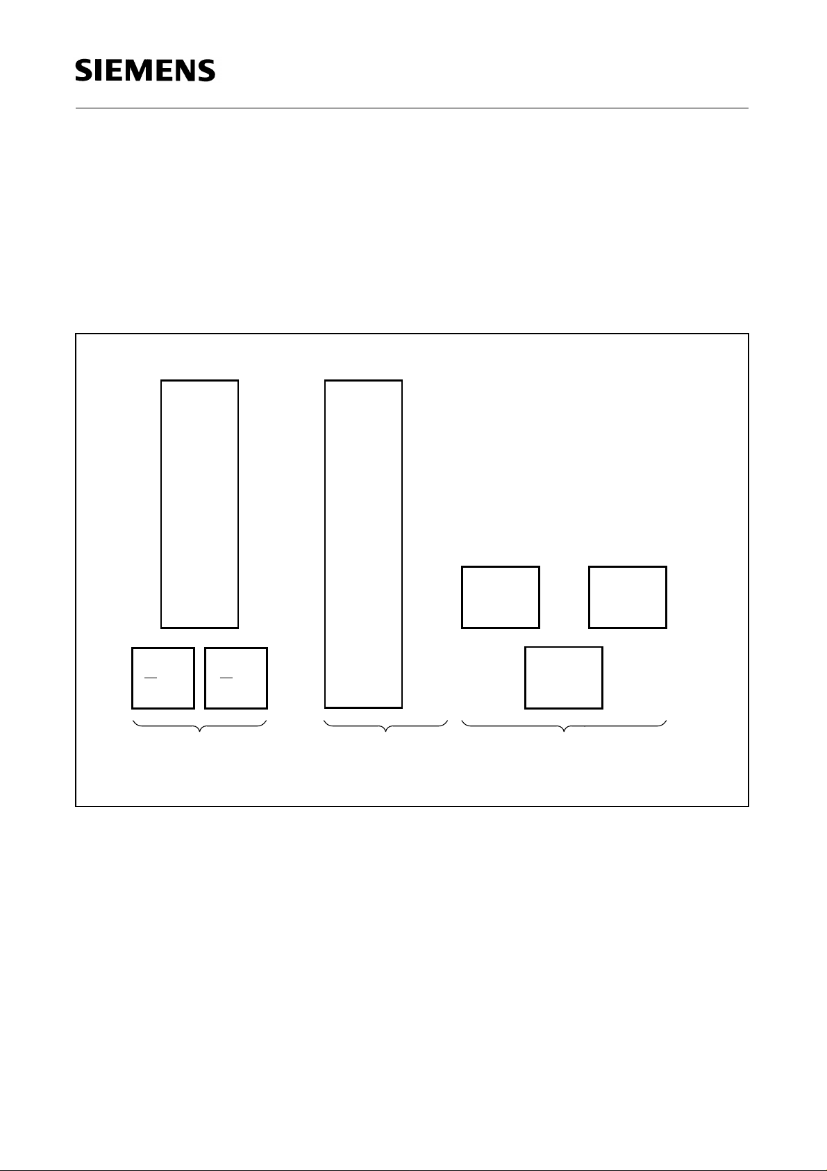
Reset and System Clock
The reset input is an active low input at pin RESET. Since the reset is synchronized internally, the
RESET pin must be held low for at least two machine cycles (24 oscillator periods) while the
oscillator is running. A pullup resistor is internally connected to V
CC
to allow a power-up reset with
an external capacitor only. An automatic reset can be obtained when V
CC
is applied by connecting
the RESET pin to V
SS
via a capacitor. Figure 6 shows the possible reset circuitries.
Figure 6
Reset Circuitries
MCS03203
RESET
C515
b)a)
c)
+
+
&
RESET
RESET
C515
C515
Semiconductor Group 17 1997-08-01
C515
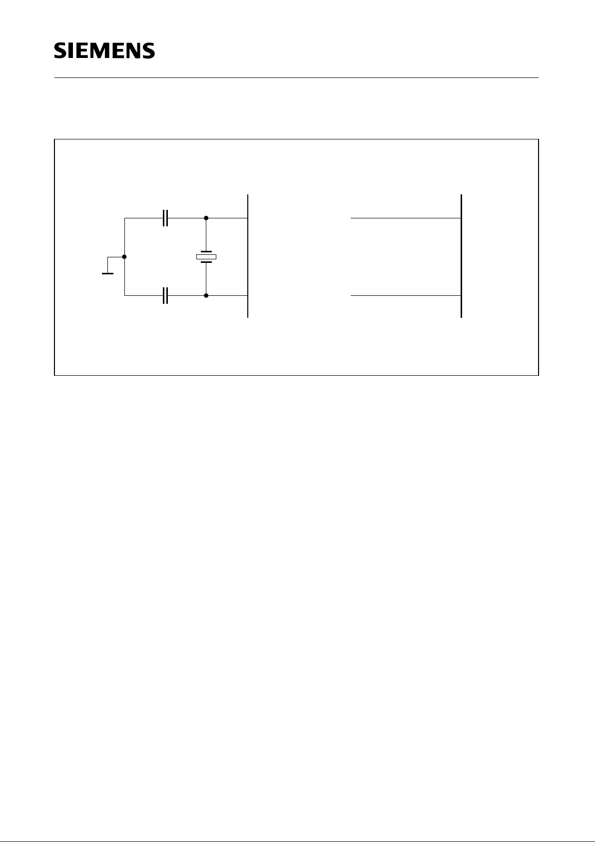
Figure 7 shows the recommended oscillator circuitries for crystal and external clock operation.
Figure 7
Recommended Oscillator Circuitries
MCS03204
XTAL1
XTAL2 XTAL2
XTAL1
Crystal Oscillator Mode Driving from External Source
External Oscillator
Signal
N.C.
1-24 MHz
C
C
C
= 20 pF±10 pF (incl. stray capacitance)
Crystal Mode :
 Loading...