


Microcomputer Components
8-Bit CMOS Microcontroller
C540U / C541U
Data Sheet 10.97

C540U/C541U Data Sheet |
|
Revision History : |
1997-10-01 |
|
|
Previous Releases : |
none (Original Version) |
Page / Chapters |
Subjects (changes since last revision) |
|
|
|
|
Edition 1997-10-01
Published by Siemens AG, Bereich Halbleiter, MarketingKommunikation, Balanstraße 73, 81541 München
© Siemens AG 1997.
All Rights Reserved.
Attention please!
As far as patents or other rights of third parties are concerned, liability is only assumed for components, not for applications, processes and circuits implemented within components or assemblies.
The information describes the type of component and shall not be considered as assured characteristics. Terms of delivery and rights to change design reserved.
For questions on technology, delivery and prices please contact the Semiconductor Group Offices in Germany or the Siemens Companies and Representatives worldwide (see address list).
Due to technical requirements components may contain dangerous substances. For information on the types in question please contact your nearest Siemens Office, Semiconductor Group.
Siemens AG is an approved CECC manufacturer.
Packing
Please use the recycling operators known to you. We can also help you – get in touch with your nearest sales office. By agreement we will take packing material back, if it is sorted. You must bear the costs of transport.
For packing material that is returned to us unsorted or which we are not obliged to accept, we shall have to invoice you for any costs incurred.
Components used in life-support devices or systems must be expressly authorized for such purpose!
Critical components1 of the Semiconductor Group of Siemens AG, may only be used in life-support devices or systems2 with the express written approval of the Semiconductor Group of Siemens AG.
1A critical component is a component used in a life-support device or system whose failure can reasonably be expected to cause the failure of that life-support device or system, or to affect its safety or effectiveness of that device or system.
2Life support devices or systems are intended (a) to be implanted in the human body, or (b) to support and/or maintain and sustain human life. If they fail, it is reasonable to assume that the health of the user may be endangered.
8-Bit CMOS Microcontroller |
C540U |
|
C541U |
Advance Information
•Enhanced 8-bit C500 CPU
–Full software/toolset compatible to standard 80C51/80C52 microcontrollers
•12 MHz external operating frequency
–500 ns instruction cycle
•Built-in PLL for USB synchronization
•On-chip OTP program memory
–C540U : 4K byte
–C541U : 8K byte
–Alternatively up to 64K byte external program memory
–Optional memory protection
•On-chip USB module
–Compliant to USB specification
–Full speed or low speed operation
–Five endpoints : one bidirectional control endpoint
four versatile programmable endpoints
–Registers are located in special function register area
–On-chip USB transceiver
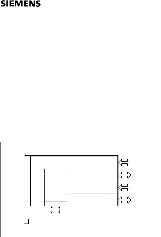
On-Chip Emulation Support Module
Oscillator |
Watchdog |
Watchdog |
Timer |
|
|
SSC
Power
Saving
Modes USB
Module
USB Transceiver
RAM 256 x 8
T0
CPU
T1
OTP Prog. Memory C540U : 4 k x 8 C541U : 8 k x 8
Port 0 |
I/O |
Port 1 |
I/O |
Port 2 |
I/O |
Port 3 |
I/O |
D+ D-
The shaded units are not available in the C540U. |
MCA03373 |
Semiconductor Group |
3 |
1997-10-01 |

C540U
C541U
Features (cont’d) :
•Up to 64K byte external data memory
•256 byte on-chip RAM
•Four parallel I/O ports
–P-LCC-44 package : three 8-bit ports and one 6-bit port
–P-SDIP-52 package : four 8-bit ports
–LED current drive capability for 3 pins (10 mA)
•Two 16-bit timer/counters (C501 compatible)
•SSC synchronous serial interface (SPI compatible) (only C541U)
–Master and slave capable
–Programmable clock polarity / clock-edge to data phase relation
–LSB/MSB first selectable
–1.5 MBaud transfer rate at 12 MHz operating frequency
•7 interrupt sources (2 external, 5 internal with 2 USB interrupts) selectable at 2 priority levels
•Enhanced fail safe mechanisms
–Programmable watchdog timer (only C541U)
–Oscillator watchdog
•Power saving modes
–idle mode
–software power down mode with wake-up capability through INT0 pin or USB
•On-chip emulation support logic (Enhanced Hooks Technology TM)
•P-LCC-44 and P-SDIP-52 packages
•Power supply voltage range : 4.0V to 5.5V
• Temperature Range : |
SAB-C540U |
TA = 0 to 70 °C |
|||
|
|
SAB-C541U |
TA = 0 to 70 °C |
||
Table 1 |
|
|
|
|
|
Ordering Information |
|
|
|
|
|
|
|
|
|
|
|
Type |
Ordering Code |
Package |
|
Description |
|
|
|
|
|
|
(8-Bit CMOS microcontroller) |
|
|
|
|
|
|
SAB-C540U-EN |
Q67126-C2042 |
P-LCC-44-2 |
|
8-Bit CMOS microcontroller (12 MHz) |
|
|
|
|
|
|
|
SAB-C540U-EP |
Q67120-C2043 |
P-SDIP-52-1 |
|
8-Bit CMOS microcontroller (12 MHz) |
|
|
|
|
|
|
|
SAB-C541U-1EN |
Q67126-C2001 |
P-LCC-44-2 |
|
8-Bit CMOS microcontroller (12 MHz) |
|
|
|
|
|
|
|
SAB-C541U-1EP |
Q67120-C2021 |
P-SDIP-52-1 |
|
8-Bit CMOS microcontroller (12 MHz) |
|
|
|
|
|
|
|
Semiconductor Group |
4 |
1997-10-01 |

C540U
C541U
|
|
|
|
|
|
|
V CC |
V SS |
|
|
||||
XTAL2 |
|
|
|
|
|
|
|
|
|
Port |
0 |
|||
|
|
|
|
|
|
|
|
|||||||
|
|
|
|
|
|
|
|
|||||||
|
|
|
|
|
|
|
|
|
|
|
|
|
||
XTAL1 |
|
|
|
|
|
|
|
|
|
8-Bit Digital I / O |
||||
|
|
|
|
|
|
|
|
|||||||
ALE |
|
|
|
|
|
|
|
|
|
Port |
1 |
|||
|
|
|
|
|
|
|
|
P-LCC-44 : 6-Bit Digital I / O |
||||||
|
|
|
|
|
|
|
|
|
|
|
|
|
||
PSEN |
|
|
|
|
C540U |
P-SDIP-52 : 8-Bit Digital I / O |
||||||||
|
|
|
|
|||||||||||
|
|
|
|
|
|
|
|
|
C541U |
|
|
|||
EA |
|
|
|
|
Port |
2 |
||||||||
|
|
|
|
|
|
|
|
|
|
|||||
|
|
|
|
|
|
|
|
|
|
|
|
|
||
RESET |
|
|
|
|
|
|
|
|
|
|
8-Bit Digital I / O |
|||
|
|
|
|
|
|
|
|
|
||||||
D+ |
|
|
|
|
|
|
|
|
Port |
3 |
||||
|
|
|
|
|
|
|
|
8-Bit Digital I / O |
||||||
D- |
|
|
|
|
|
|
|
|
||||||
|
|
|
|
|
|
|
|
|
MCL03374 |
|||||
|
|
|
|
|
|
|
|
|||||||
|
|
|
|
|
|
|
|
|
|
|
|
|
|
|
Figure 2
Logic Symbol
Additional Literature
For further information about the C540U/C541U the following literature is available :
Title |
|
Ordering Number |
|
|
|
C540U/C541U 8-Bit CMOS Microcontroller User’s Manual |
B158-H????-X-X-7600 |
|
|
|
|
C500 |
Microcontroller Family |
B158-H6987-X-X-7600 |
Architecture and Instruction Set User’s Manual |
|
|
|
|
|
C500 |
Microcontroller Family - Pocket Guide |
B158-H6986-X-X-7600 |
|
|
|
Semiconductor Group |
5 |
1997-10-01 |
C540U
C541U
|
|
|
|
|
|
|
|
|
/ LED1 |
/ LED0 |
|
|
|
|
|
/ AD0 |
/ AD1 |
/ AD2 |
/ AD3 |
|
|
|
|
|
|
|
|
|
|
|
|
|
|
|
|
|
SLS |
|
|
|
|
||||||
|
|
|
|
|
|
|
|
|
|
|
SSU |
CCU |
/ |
|
|
|
|
||||||
|
|
|
|
|
|
|
|
|
P1.1 |
P1.0 |
D- |
D+ |
P1.5 |
P0.0 |
P0.1 |
P0.2 |
P0.3 |
|
|
|
|
||
|
|
|
|
|
|
|
|
|
V V |
|
|
|
|
||||||||||
|
|
|
|
|
|
|
|
6 |
5 |
4 |
3 |
2 |
1 |
44 |
43 |
42 |
41 |
40 |
|
|
|
|
|
|
P1.2 / |
|
|
|
|
7 |
|
|
|
|
|
|
|
|
|
|
39 |
P0.4 |
/ AD4 |
||||
SCLK |
|
|
|
|
|
|
|
|
|
||||||||||||||
|
|
|
|
VCC |
8 |
|
|
|
|
|
|
|
|
|
|
38 |
P0.5 |
/ AD5 |
|||||
|
|
|
|
|
VSS |
9 |
|
|
|
|
|
|
|
|
|
|
37 |
P0.6 |
/ AD6 |
||||
|
|
RESET |
10 |
|
|
|
|
|
|
|
|
|
36 |
P0.7 |
/ AD7 |
||||||||
|
P3.0 / LED2 |
11 |
|
|
|
C540U |
|
|
|
35 |
EA |
|
|
|
|||||||||
|
|
|
|
|
|
|
12 |
|
|
|
|
|
|
34 |
|
|
|
|
|||||
|
P1.3 / |
SRI |
|
|
|
|
|
|
P1.4 |
/ |
STO |
||||||||||||
P3.1 / DADD |
13 |
|
|
|
C541U |
|
|
|
33 |
ALE |
|
|
|||||||||||
|
|
|
|
|
|
|
|
|
|
|
|
|
|
|
|
|
|
|
|
||||
|
P3.2 / INT0 |
14 |
|
|
|
|
|
|
|
|
|
32 |
PSEN |
||||||||||
|
|
|
|
|
|
|
|
|
|
|
|
|
|
|
|
|
|
|
|
|
|||
|
P3.3 / INT1 |
15 |
|
|
|
|
|
|
|
|
|
31 |
P2.7 |
/ A15 |
|||||||||
|
P3.4 / T0 |
16 |
|
|
|
|
|
|
|
|
|
30 |
P2.6 |
/ A14 |
|||||||||
|
P3.5 / T1 |
17 |
|
|
|
|
|
|
|
|
|
29 |
P2.5 |
/ A13 |
|||||||||
|
|
|
|
|
|
|
|
18 |
19 |
20 |
21 |
22 |
23 |
24 |
25 |
26 |
27 |
28 |
|
|
|
|
|
|
|
|
|
|
|
|
|
|
WR/P3.6 |
RD/P3.7 |
XTAL2 |
XTAL1 |
V |
V |
A8/P2.0 |
A9/P2.1 |
A10/P2.2 |
A11/P2.3 |
A12/P2.4 |
|
|
|
|
|
|
|
|
|
|
|
|
|
|
|
|
|
SS |
CC |
|
|
|
|
|
|
|
|
|
|
|
|
|
|
|
|
|
|
|||||||||||||||
|
|
|
|
|
|
|
|
|
|
|
|
|
|
|
|
|
|
|
|
|
|
|
|
|
|
This pin functionality ist not available for the C540U. |
MCP03343 |
||||||||||||||||||||
|
|
||||||||||||||||||||||
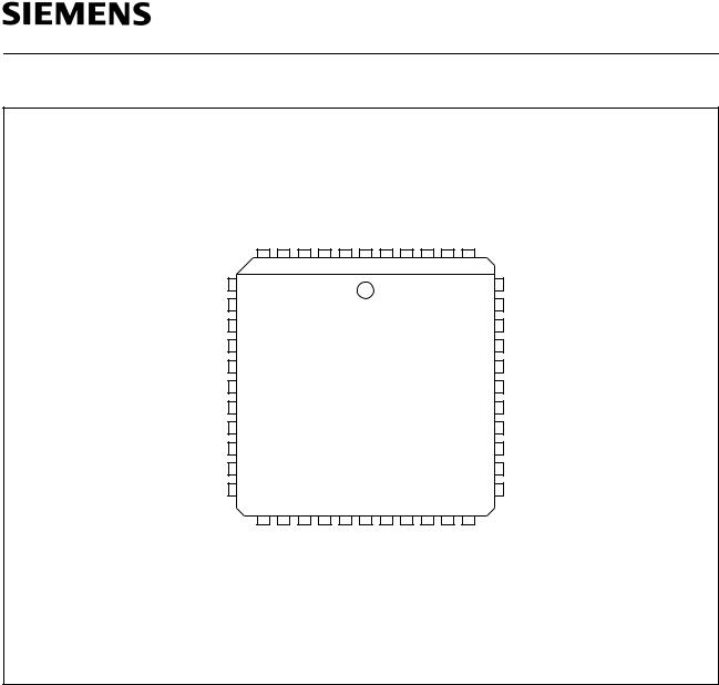
Figure 3
Pin Configuration P-LCC-44 Package (top view)
Semiconductor Group |
6 |
1997-10-01 |
C540U
C541U
|
VCCU |
|
1 |
|||||
|
|
|||||||
|
VSSU |
|
2 |
|||||
|
|
|||||||
|
|
|
|
D+ |
|
3 |
||
|
|
|
|
|||||
|
|
|
|
D- |
|
4 |
||
|
|
|
|
|||||
|
|
N.C. |
|
5 |
||||
|
|
|||||||
|
|
N.C. |
|
6 |
||||
|
|
|||||||
P1.0 / LED0 |
|
7 |
||||||
|
||||||||
P1.1 / LED1 |
|
8 |
||||||
|
||||||||
|
|
|
|
|
|
|
|
|
P1.2 / |
SCLK |
|
9 |
|||||
|
|
VCC |
|
10 |
||||
|
|
|
||||||
|
|
|||||||
|
|
|
VSS |
|
11 |
|||
|
|
|
|
|||||
RESET |
|
12 |
||||||
|
||||||||
P3.0 / LED2 |
|
13 |
||||||
|
||||||||
|
|
|
|
|
|
|
|
|
P1.3 / |
SRI |
|
14 |
|||||
|
|
P1.6 |
|
15 |
||||
|
|
|
||||||
|
|
|||||||
P3.1 / DADD |
|
16 |
||||||
|
||||||||
|
|
|
|
|
|
|
|
|
P3.2 / INT0 |
|
17 |
||||||
|
||||||||
|
|
|
|
|
|
|||
P3.3 / |
INT1 |
|
|
|
18 |
|||
P3.4 / T0 |
|
19 |
||||||
|
||||||||
P3.5 / T1 |
|
20 |
||||||
|
||||||||
|
|
|
|
|
|
|||
P3.6 / WR |
|
21 |
||||||
|
||||||||
|
|
|
|
|
||||
P3.7 / RD |
|
22 |
||||||
|
||||||||
XTAL2 |
|
23 |
||||||
|
||||||||
XTAL1 |
|
24 |
||||||
|
||||||||
|
|
|
VSS |
|
25 |
|||
|
|
|
|
|||||
|
|
VCC |
|
26 |
||||
|
|
|||||||
|
|
|
|
|
|
|
|
|
|
52 |
|
|
N.C. |
|
|
|
|
|
|
|
|
|
|
|
|
|
|
|
|
|
|
51 |
|
|
P1.5 |
/ |
SLS |
||||
|
|
|||||||||
|
50 |
|
|
P0.0 |
/ AD0 |
|||||
|
|
|
||||||||
|
|
|||||||||
|
49 |
|
|
P0.1 |
/ AD1 |
|||||
|
|
|||||||||
|
48 |
|
|
P0.2 |
/ AD2 |
|||||
|
|
|||||||||
|
47 |
|
|
P0.3 |
/ AD3 |
|||||
|
|
|||||||||
|
46 |
|
|
P0.4 |
/ AD4 |
|||||
|
|
|||||||||
|
45 |
|
|
P0.5 |
/ AD5 |
|||||
|
|
|||||||||
|
44 |
|
|
P0.6 |
/ AD6 |
|||||
|
|
|||||||||
|
43 |
|
|
P0.7 |
/ AD7 |
|||||
|
|
|||||||||
|
|
|
|
|
|
|
|
|
|
|
|
42 |
|
|
EA |
|
|
|
|
|
|
|
|
|
|
|
|
|
||||
|
|
|
|
|
|
|
|
|
|
|
|
41 |
|
|
P1.4 |
/ |
STO |
||||
|
|
|||||||||
C540U |
40 |
|
|
P1.7 |
|
|
|
|
|
|
|
|
|
|
|
|
|
||||
C541U |
39 |
|
|
ALE |
|
|
|
|
|
|
|
|
|
|
|
|
|
||||
|
38 |
|
|
PSEN |
||||||
|
37 |
|
|
N.C. |
|
|
|
|
|
|
|
36 |
|
|
N.C. |
|
|
|
|
|
|
|
35 |
|
|
P2.7 |
/ A15 |
|||||
|
34 |
|
|
P2.6 |
/ A14 |
|||||
|
33 |
|
|
P2.5 |
/ A13 |
|||||
|
32 |
|
|
P2.4 |
/ A12 |
|||||
|
31 |
|
|
P2.3 |
/ A11 |
|||||
|
30 |
|
|
P2.2 |
/ A10 |
|||||
|
29 |
|
|
P2.1 |
/ A9 |
|||||
|
28 |
|
|
P2.0 |
/ A8 |
|||||
|
27 |
|
|
N.C. |
|
|
|
|
|
|
MCP03344
 This pin functionality ist not available for the C540U.
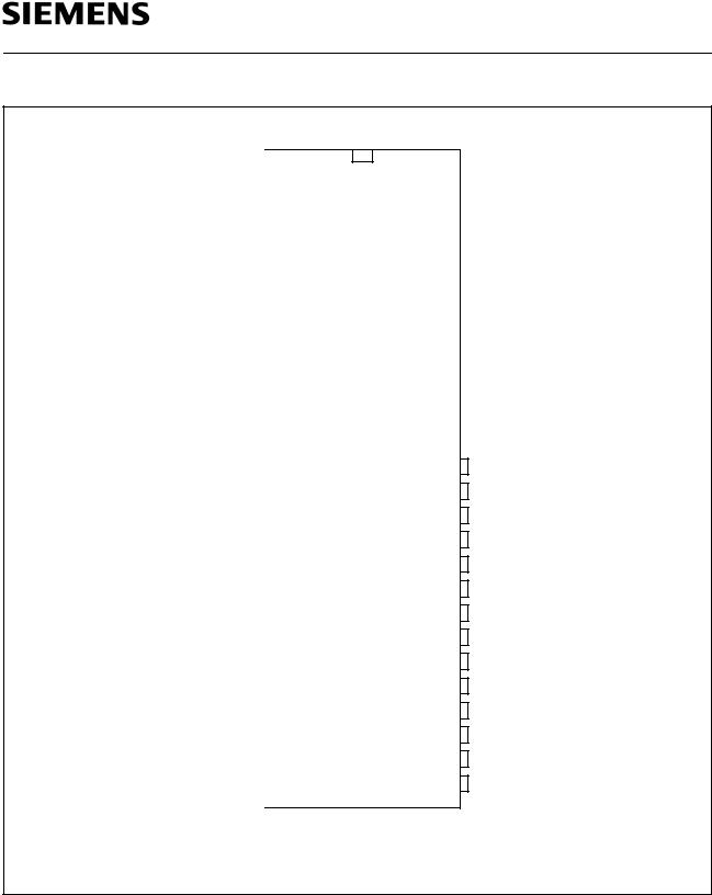
Figure 4
Pin Configuration P-SDIP-52 Package (top view)
Semiconductor Group |
7 |
1997-10-01 |

C540U
C541U
Table 2
Pin Definitions and Functions
Symbol |
|
|
Pin Numbers |
I/O*) |
Function |
|
|||
|
|
|
|
|
|
|
|
||
|
|
P-LCC-44 |
P-SDIP-52 |
|
|
|
|
|
|
|
|
|
|
|
|
|
|||
D+ |
|
3 |
|
3 |
I/O |
USB D+ Data Line |
|||
|
|
|
|
|
|
The pin D+ can be directly connected to USB cable |
|||
|
|
|
|
|
|
(transceiver is integrated on-chip). |
|||
|
|
|
|
|
|
|
|||
D- |
|
4 |
|
4 |
I/O |
USB D- Data Line |
|||
|
|
|
|
|
|
The pin D- can be directly connected to USB cable |
|||
|
|
|
|
|
|
(transceiver is integrated on-chip). |
|||
|
|
|
|
|
|
|
|
|
|
P1.0 - P1.4 |
|
5 - 7, |
|
7 - 9, 14, 41, |
I/O |
Port 1 |
|
|
|
|
|
12, 34, 44 |
51, 15, 40 |
|
is an 6-bit (P-LCC-44) or 8-bit (P-SDIP-52) quasi- |
||||
|
|
|
|
|
|
bidirectional I/O port with internal pullup resistors. |
|||
|
|
|
|
|
|
Port 1 pins that have 1's written to them are pulled |
|||
|
|
|
|
|
|
high by the internal pullup resistors, and in that |
|||
|
|
|
|
|
|
state can be used as inputs. As inputs, port 1 pins |
|||
|
|
|
|
|
|
being externally pulled low will source current (I IL, |
|||
|
|
|
|
|
|
in the DC characteristics) because of the internal |
|||
|
|
|
|
|
|
pullup resistors. |
|||
|
|
|
|
|
|
Port 1 also contains two outputs with LED drive |
|||
|
|
|
|
|
|
capability as well as the four pins of the SSC |
|||
|
|
|
|
|
|
(C541U only). The output latch corresponding to a |
|||
|
|
|
|
|
|
secondary function must be programmed to a one |
|||
|
|
|
|
|
|
(1) for that function to operate (except when used |
|||
|
|
|
|
|
|
for the compare functions). The secondary |
|||
|
|
|
|
|
|
functions are assigned to the port 1 pins as follows : |
|||
|
|
5 |
|
7 |
|
P1.0 / |
LED0 LED0 output |
||
|
|
6 |
|
8 |
|
P1.1 / |
LED1 LED1 output |
||
|
|
7 |
|
9 |
|
P1.2 / |
SCLK SSC Master Clock Output / |
||
|
|
|
|
|
|
|
|
|
SSC Slave Clock Input (C541U only) |
|
|
12 |
|
13 |
|
P1.3 / |
SRI |
SSC Receive Input (C541U only) |
|
|
|
34 |
|
41 |
|
P1.4 / |
STO |
SSC Transmit Output (C541U only) |
|
|
|
44 |
|
51 |
|
P1.5 / |
|
|
SSC Slave Select Inp. (C541U only) |
|
|
|
SLS |
||||||
|
|
– |
|
15 |
|
P1.6 |
|
|
(P-SDIP-52 only) |
|
|
– |
|
40 |
|
P1.7 |
|
|
(P-SDIP-52 only) |
|
|
|
|
|
|
|
|
||
RESET |
|
10 |
|
12 |
I |
RESET |
|
||
|
|
|
|
|
|
A high level on this pin for the duration of two |
|||
|
|
|
|
|
|
machine cycles while the oscillator is running |
|||
|
|
|
|
|
|
resets the C540U/C541U. A small internal pulldown |
|||
|
|
|
|
|
|
resistor permits power-on reset using only a |
|||
|
|
|
|
|
|
capacitor connected to VCC . |
|||
*) I = Input |
|
|
|
|
|
|
|
|
|
O = Output |
|
|
|
|
|
|
|
|
|
Semiconductor Group |
8 |
1997-10-01 |

C540U
C541U
Table 2
Pin Definitions and Functions (cont’d)
Symbol |
|
Pin Numbers |
I/O*) |
Function |
|
|
|
||||||
|
|
|
|
|
|
|
|
|
|
|
|
|
|
|
|
P-LCC-44 |
P-SDIP-52 |
|
|
|
|
|
|
|
|
|
|
|
|
|
|
|
|
|
|
|
|||||
P3.0 - P3.7 |
|
11, 13 - 19 |
13, 16 - 22 |
I/O |
Port 3 |
|
|
|
|||||
|
|
|
|
|
is an 8-bit quasi-bidirectional I/O port with internal |
||||||||
|
|
|
|
|
pullup resistors. Port 3 pins that have 1's written to |
||||||||
|
|
|
|
|
them are pulled high by the internal pullup resistors, |
||||||||
|
|
|
|
|
and in that state can be used as inputs. As inputs, |
||||||||
|
|
|
|
|
port 3 pins being externally pulled low will source |
||||||||
|
|
|
|
|
current (I IL, in the DC characteristics) because of |
||||||||
|
|
|
|
|
the internal pullup resistors. Port 3 also contains |
||||||||
|
|
|
|
|
the interrupt, timer, serial port and external memory |
||||||||
|
|
|
|
|
strobe pins that are used by various options. The |
||||||||
|
|
|
|
|
output latch corresponding to a secondary function |
||||||||
|
|
|
|
|
must be programmed to a one (1) for that function |
||||||||
|
|
|
|
|
to operate. The secondary functions are assigned |
||||||||
|
|
|
|
|
to the pins of port 3, as follows: |
||||||||
|
|
|
|
|
P3.0 / LED2 |
LED2 output |
|||||||
|
|
|
|
|
P3.1 / DADD |
Device attached input |
|||||||
|
|
|
|
|
P3.2 / |
|
|
|
|
|
External interrupt 0 input / |
||
|
|
|
|
|
INT0 |
||||||||
|
|
|
|
|
|
|
|
|
|
|
timer 0 gate control input |
||
|
|
|
|
|
P3.3 / |
|
|
|
|
External interrupt 1 input / |
|||
|
|
|
|
|
INT1 |
||||||||
|
|
|
|
|
|
|
|
|
|
|
timer 1 gate control input |
||
|
|
|
|
|
P3.4 / T0 |
Timer 0 counter input |
|||||||
|
|
|
|
|
P3.5 / T1 |
Timer 1 counter input |
|||||||
|
|
|
|
|
P3.6 / |
|
|
|
|
|
control output; latches the |
||
|
|
|
|
|
WR |
WR |
|||||||
|
|
|
|
|
|
|
|
|
|
|
data byte from port 0 into the |
||
|
|
|
|
|
|
|
|
|
|
|
external data memory |
||
|
|
|
|
|
P3.7 / |
|
|
|
control output; enables the |
||||
|
|
|
|
|
RD |
RD |
|||||||
|
|
|
|
|
|
|
|
|
|
|
external data memory |
||
|
|
|
|
|
|
|
|
|
|||||
XTAL2 |
|
20 |
23 |
– |
XTAL2 |
|
|
|
|||||
|
|
|
|
|
is the output of the inverting oscillator amplifier. |
||||||||
|
|
|
|
|
This pin is used for the oscillator operation with |
||||||||
|
|
|
|
|
crystal or ceramic resonator. |
||||||||
|
|
|
|
|
|
|
|
|
|||||
XTAL1 |
|
21 |
24 |
– |
XTAL1 |
|
|
|
|||||
|
|
|
|
|
is the input to the inverting oscillator amplifier and |
||||||||
|
|
|
|
|
input to the internal clock generator circuits. |
||||||||
|
|
|
|
|
To drive the device from an external clock source, |
||||||||
|
|
|
|
|
XTAL1 should be driven, while XTAL2 is left |
||||||||
|
|
|
|
|
unconnected. Minimum and maximum high and |
||||||||
|
|
|
|
|
low times as well as rise/fall times specified in the |
||||||||
|
|
|
|
|
AC characteristics must be observed. |
||||||||
|
|
|
|
|
|
|
|
|
|
|
|
|
|
*) I = Input |
|
|
|
|
|
|
|
|
|
|
|
|
|
O = Output |
|
|
|
|
|
|
|
|
|
|
|
|
|
Semiconductor Group |
|
|
9 |
|
|
|
|
|
1997-10-01 |
||||

C540U
C541U
Table 2 |
|
|
|
|
|
|
|
|
|
|||
Pin Definitions and Functions |
(cont’d) |
|
|
|
|
|||||||
|
|
|
|
|
|
|
||||||
Symbol |
|
Pin Numbers |
|
I/O*) |
|
Function |
||||||
|
|
|
|
|
|
|
|
|
|
|
||
|
|
|
|
P-LCC-44 |
P-SDIP-52 |
|
|
|
|
|
|
|
|
|
|
|
|
|
|
|
|||||
P2.0 - P2.7 |
|
24 - 31 |
28 - 35 |
|
I/O |
|
Port 2 |
|||||
|
|
|
|
|
|
|
|
|
is an 8-bit quasi-bidirectional I/O port with internal |
|||
|
|
|
|
|
|
|
|
|
pullup resistors. Port 2 pins that have 1's written to |
|||
|
|
|
|
|
|
|
|
|
them are pulled high by the internal pullup resistors, |
|||
|
|
|
|
|
|
|
|
|
and in that state can be used as inputs. As inputs, |
|||
|
|
|
|
|
|
|
|
|
port 2 pins being externally pulled low will source |
|||
|
|
|
|
|
|
|
|
|
current (I IL, in the DC characteristics) because of |
|||
|
|
|
|
|
|
|
|
|
the internal pullup resistors. |
|||
|
|
|
|
|
|
|
|
|
Port 2 emits the high-order address byte during |
|||
|
|
|
|
|
|
|
|
|
fetches from external program memory and during |
|||
|
|
|
|
|
|
|
|
|
accesses to external data memory that use 16-bit |
|||
|
|
|
|
|
|
|
|
|
addresses (MOVX @DPTR). In this application it |
|||
|
|
|
|
|
|
|
|
|
uses strong internal pullup resistors when issuing |
|||
|
|
|
|
|
|
|
|
|
1's. During accesses to external data memory that |
|||
|
|
|
|
|
|
|
|
|
use 8-bit addresses (MOVX @Ri), port 2 issues the |
|||
|
|
|
|
|
|
|
|
|
contents of the P2 special function register. |
|||
|
|
|
|
|
|
|
|
|
|
|
|
|
|
|
|
|
32 |
38 |
|
O |
|
The |
|
|
|
PSEN |
Program Store Enable |
|||||||||||
|
|
|
|
|
|
|
|
|
output is a control signal that enables the external |
|||
|
|
|
|
|
|
|
|
|
program memory to the bus during external fetch |
|||
|
|
|
|
|
|
|
|
|
operations. It is activated every six oscillator |
|||
|
|
|
|
|
|
|
|
|
periods except during external data memory |
|||
|
|
|
|
|
|
|
|
|
accesses. The signal remains high during internal |
|||
|
|
|
|
|
|
|
|
|
program execution. |
|||
|
|
|
|
|
|
|
|
|||||
ALE |
|
33 |
39 |
|
O |
|
The Address Latch enable |
|||||
|
|
|
|
|
|
|
|
|
output is used for latching the address into external |
|||
|
|
|
|
|
|
|
|
|
memory during normal operation. It is activated |
|||
|
|
|
|
|
|
|
|
|
every six oscillator periods except during an |
|||
|
|
|
|
|
|
|
|
|
external data memory access. |
|||
|
|
|
|
|
|
|
|
|
|
|||
|
|
|
35 |
42 |
|
I |
|
|
|
|
||
EA |
External Access Enable |
|||||||||||
|
|
|
|
|
|
|
|
|
When held high, the C540U/C541U executes |
|||
|
|
|
|
|
|
|
|
|
instructions from the internal ROM as long as the |
|||
|
|
|
|
|
|
|
|
|
PC is less than 1000H for the C540U or less than |
|||
|
|
|
|
|
|
|
|
|
2000H for the C541U. When held low, the C540U/ |
|||
|
|
|
|
|
|
|
|
|
C541U fetches all instructions from external |
|||
|
|
|
|
|
|
|
|
|
program memory. For the C540U-L/C541U-L this |
|||
|
|
|
|
|
|
|
|
|
pin must be tied low. |
|||
|
|
|
|
|
|
|
|
|
|
|
||
*) I = Input |
|
|
|
|
|
|
|
|
|
|||
|
O = Output |
|
|
|
|
|
|
|
|
|
||
Semiconductor Group |
10 |
1997-10-01 |
C540U
C541U
Table 2 |
|
|
|
|
|
|
Pin Definitions and Functions |
(cont’d) |
|
||||
|
|
|
|
|
|
|
Symbol |
|
Pin Numbers |
|
I/O*) |
Function |
|
|
|
|
|
|
||
|
|
P-LCC-44 |
P-SDIP-52 |
|
|
|
|
|
|
|
|
|
|
P0.0 - P0.7 |
|
44 - 36 |
50 - 43 |
|
I/O |
Port 0 |
|
|
|
|
|
|
is an 8-bit open-drain bidirectional I/O port. Port 0 |
|
|
|
|
|
|
pins that have 1's written to them float, and in that |
|
|
|
|
|
|
state can be used as high-impedance inputs. Port 0 |
|
|
|
|
|
|
is also the multiplexed low-order address and data |
|
|
|
|
|
|
bus during accesses to external program and data |
|
|
|
|
|
|
memory. In this application it uses strong internal |
|
|
|
|
|
|
pullup resistors when issuing 1's. |
|
|
|
|
|
|
|
VCCU |
|
1 |
1 |
|
– |
Supply voltage |
|
|
|
|
|
|
for the on-chip USB transceiver circuitry. |
|
|
|
|
|
|
|
VSSU |
|
2 |
2 |
|
– |
Ground (0V) |
|
|
|
|
|
|
for the on-chip USB transceiver circuitry. |
|
|
|
|
|
|
|
VCC |
|
8, 23 |
10, 26 |
|
– |
Supply voltage |
|
|
|
|
|
|
for ports and internal logic circuitry during normal, |
|
|
|
|
|
|
idle, and power down mode. |
|
|
|
|
|
|
|
VSS |
|
9, 22 |
11, 25 |
|
– |
Ground (0V) |
|
|
|
|
|
|
for ports and internal logic circuitry during normal, |
|
|
|
|
|
|
idle, and power down mode. |
|
|
|
|
|
|
|
*) I = Input |
|
|
|
|
|
|
O = Output |
|
|
|
|
|
|
Semiconductor Group |
11 |
1997-10-01 |

C540U
C541U
|
Oscillator Watchdog |
RAM |
OTP Memory |
|
|
|
|
|
|
|
|
XTAL2 |
|
OSC & Timing |
256 x 8 |
4k x 8 (C540U) |
|
XTAL1 |
|
8k x 8 (C541U) |
|
||
|
|
|
|||
|
|
|
|
|
|
ALE |
|
|
|
|
|
PSEN |
|
CPU |
|
|
|
|
|
|
|
|
|
EA |
|
|
|
Emulation |
|
RESET |
|
Progr. Watchdog |
|
Support |
|
|
|
Logic |
|
||
Timer (C541U only) |
|
|
|||
|
|
|
|||
|
|
|
|
||
|
|
Timer 0 |
|
Port 0 |
Port 0 |
|
|
|
8-Bit Digit. I/O |
||
|
|
|
|
|
|
|
|
Timer 1 |
|
|
Port 1 |
|
|
|
|
Port 1 |
|
|
SSC (SPI) Interface |
|
6- / 8-Bit Digit. I/O 1) |
||
|
|
|
|
||
|
|
(C541U only) |
|
|
Port 2 |
|
|
|
|
Port 2 |
|
|
|
PLL |
|
8-Bit Digit. I/O |
|
|
Transceiver |
|
|
||
|
|
|
|
||
D+ |
USB |
|
|
Port 3 |
|
D- |
Module |
|
Port 3 |
||
|
8-Bit Digit. I/O |
||||
|
|
|
|
||
|
|
|
|
|
|
|
|
Interrupt Unit |
|
C540U |
|
|
|
|
C541U |
|
|
|
|
|
|
|
|
1) P-LCC-44 : 6-Bit Port; P-SDIP-52 : 8-Bit Port |
|
MCB03345 |
|||
Figure 5
Block Diagram of the C540U/C541U
Semiconductor Group |
12 |
1997-10-01 |

C540U
C541U
CPU
The C540U/C541U is efficient both as a controller and as an arithmetic processor. It has extensive facilities for binary and BCD arithmetic and excels in its bit-handling capabilities. Efficient use of program memory results from an instruction set consisting of 44 % one-byte, 41 % two-byte, and 15% threebyte instructions. With a 12 MHz crystal, 58% of the instructions are executed in 500ns.
Special Function Register PSW (Address D0H) |
|
|
Reset Value : 00H |
||||||
Bit No. |
MSB |
|
|
|
|
|
|
LSB |
|
|
D7H |
D6H |
D5H |
D4H |
D3H |
D2H |
D1H |
D0H |
|
D0H |
CY |
AC |
F0 |
RS1 |
RS0 |
OV |
F1 |
P |
PSW |
Bit |
Function |
|
|
|
|
||
CY |
Carry Flag |
|
|
|
|
||
|
Used by arithmetic instruction. |
||||||
|
|
|
|
|
|
|
|
AC |
Auxiliary Carry Flag |
|
|
|
|||
|
Used by instructions which execute BCD operations. |
||||||
|
|
|
|
|
|
|
|
F0 |
General Purpose Flag |
||||||
|
|
|
|
|
|
|
|
RS1 |
Register Bank Select Control Bits |
||||||
RS0 |
These bits are used to select one of the four register banks. |
||||||
|
|
|
|
|
|
|
|
|
|
RS1 |
|
RS0 |
Function |
|
|
|
|
|
|
|
|
|
|
|
|
0 |
|
0 |
Bank 0 selected, data address 00H-07H |
|
|
|
|
0 |
|
1 |
Bank 1 selected, data address 08H-0FH |
|
|
|
|
1 |
|
0 |
Bank 2 selected, data address 10H-17H |
|
|
|
|
1 |
|
1 |
Bank 3 selected, data address 18H-1FH |
|
|
|
|
|
|
|
|
|
|
|
|
|
|
|
|
|
|
OV |
Overflow Flag |
|
|
|
|||
|
Used by arithmetic instruction. |
||||||
|
|
|
|
|
|
|
|
F1 |
General Purpose Flag |
||||||
|
|
|
|
|
|
|
|
P |
Parity Flag |
|
|
|
|
||
Set/cleared by hardware after each instruction to indicate an odd/even number of "one" bits in the accumulator, i.e. even parity.
Semiconductor Group |
13 |
1997-10-01 |
C540U
C541U
Memory Organization
The C540U/C541U CPU manipulates operands in the following four address spaces:
–8 or 4 KByte on-chip OTP program memory
–Totally up to 64 Kbyte internal/external program memory
–up to 64 Kbyte of external data memory
–256 bytes of internal data memory
–a 128 byte special function register area
Figure 6 illustrates the memory address spaces of the C540U/C541U.
FFFF H |
|
FFFFH |
|
External
External
|
|
|
|
|
|
|
|
2000 H 1) |
|
|
|
|
|
|
|
|
|
|
|
|
|
|
|||
|
|
|
|
|
|
|
|
|
1FFF H 1) |
|
|
|
Internal |
|
External |
|
|
|
|||||||
|
|
|
|
|
||||||||
|
|
|
|
|
|
|
|
|
|
|
||
(EA = 1) |
|
(EA = 0) |
|
|
|
|
||||||
|
|
|
|
|
|
|
|
|
0000H |
|
|
0000 H |
|
|
|
|
|
|
|
|
|
|
|||
|
|
|
"Code Space" |
"External Data Space" |
||||||||
1) For the C504U the int. / ext. program memory boundary is at 0FFFH / 1000H .
Indirect |
|
Direct |
|||
Addr. |
|
Addr. |
|||
|
|
FF H |
|
|
FF H |
Internal |
|
Special |
|||
|
|
|
|||
|
Function |
|
|||
RAM |
|
|
|||
|
Register |
|
|||
|
|
|
|
||
|
|
80 H |
|
|
80 H |
|
|
|
|
||
|
|
|
|
7F H |
|
|
|
Internal |
|
||
|
|
|
|
|
|
|
|
RAM |
|
|
|
|
|
|
|
00 H |
|
|
|
|
|
||
"Internal Data Space"
MCD03375
Figure 6
C540U/C541U Memory Map Memory Map
Semiconductor Group |
14 |
1997-10-01 |
C540U
C541U
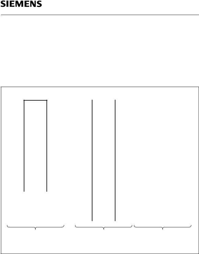
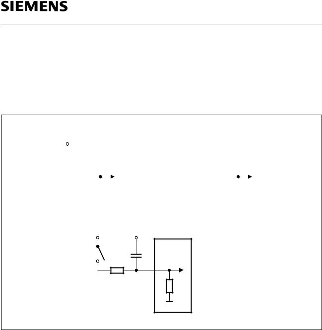
Reset and System Clock
The reset input is an active high input at pin RESET. Since the reset is synchronized internally, the RESET pin must be held high for at least two machine cycles (12 oscillator periods) while the oscillator is running. A pulldown resistor is internally connected to VSS to allow a power-up reset with an external capacitor only. An automatic reset can be obtained when VCC is applied by connecting the RESET pin to VCC via a capacitor. Figure 7 shows the possible reset circuitries.
VCC |
a) |
|
|
|
|
b) |
||||||||||
|
+ |
C540U |
|
|
|
|
C540U |
|||||||||
|
C541U |
|
|
|
|
C541U |
||||||||||
|
|
|
|
|
|
|
||||||||||
|
|
|
RESET |
|
|
& |
|
RESET |
||||||||
|
|
|
|
|
|
|||||||||||
|
|
|
|
|
|
|
|
|
|
|
|
|
|
|
|
|
|
|
|
|
|
|
|
|
|
|
|
|
|
|
|
|
|
|
|
|
|
|
|
|
|
|
|
|
|
|
|
|
|
|
|
|
|
|
|
|
|
|
|
|
|
|
|
|
|
|
|
|
|
|
|
|
|
|
|
|
|
|
|
|
|
|
|
|
|
|
|
|
|
|
|
|
|
|
|
|
|
|
|
|
|
|
|
|
|
|
|
|
|
|
|
|
|
|
|
|
|
|
VCC |
VCC |
c) |
+
C540U
C541U
RESET
MCD03376
Figure 7
Reset Circuitries
Semiconductor Group |
15 |
1997-10-01 |

C540U
C541U
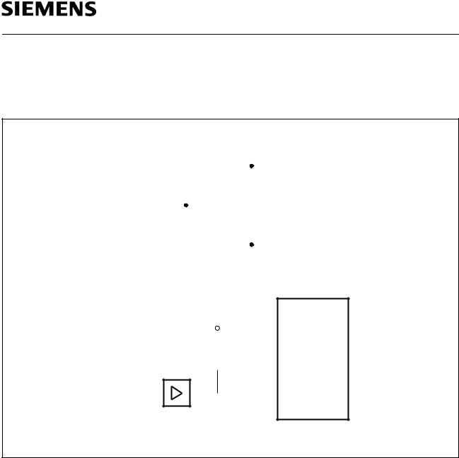
The oscillator and clock generation circuitry of the C540U/C541U is shown in figure 5-8. The crystal oscillator generates the system clock for the microcontroller. The USB module can be provided with the following clocks :
–Full speed operation : 48 MHz with a data rate of 12 Mbit/s
–Low speed operation : 6 MHz with a data rate of 1.5 Mbit/s
The low speed clock is generated by a dividing the system clock by 2. The full speed clock is generated by a PLL, which multiplies the system clock by a fix factor of 4. This PLL can be enabled or disabled by bit PCLK of SFR DCR. Depending on full or low speed operation of the USB bit SPEED of SFR has to be set or cleared for the selection of the USB clock. Bit UCLK is a general enable bit for the USB clock.
XTAL1 |
Pin |
|
|
System Clock |
|
12 MHz |
|
||
12 MHz |
Crystal |
|
of the |
|
Oscillator |
|
|
||
|
|
|
Microcontroler |
|
XTAL2 |
Pin |
|
|
|
|
|
|
||
|
|
|
|
|
|
Divider |
PLL |
Enable |
PCLK |
|
by 2 |
x 4 |
|
|
|
|
DCR.0 |
||
|
|
|
|
|
|
6 MHz |
48 MHz |
|
|
|
|
|
1 |
to USB |
|
|
|
0 |
|
|
|
|
Module |
|
|
|
|
|
|
|
|
|
SPEED |
UCLK |
|
C540U / C541U |
|
DCR.7 |
DCR.1 |
|
|
|
|
MCB03377 |
Figure 8
Block Diagram of the Clock Generation Circuitry
Semiconductor Group |
16 |
1997-10-01 |
C540U
C541U
The clock generator provides the internal clock signals to the chip. These signals define the internal phases, states and machine cycles. Figure 9 shows the recommended oscillator circuits for crystal and external clock operation.
|
|
C |
|
|||||||||
|
|
XTAL2 |
||||||||||
|
|
|
|
|
|
|
|
|
|
|
|
|
|
|
|
|
|
|
|
|
|
|
|
|
|
|
|
12 MHz |
|
|
|
|
|
|
|
C540U |
||
|
|
C |
|
|
|
|
C541U |
|||||
|
|
|
|
|||||||||
|
|
|
|
|
|
|
|
|
|
|
|
XTAL1 |
|
|
|
|
|
|
|
|
|
|
|
|
|
|
|
|||||||||||
C = 20 pF 10 pF for crystal operation |
||||||||||||
V CC |
|
C540U |
|||
|
C541U |
||||
|
|
|
N.C. |
|
XTAL2 |
|
|
|
|
||
|
|
|
|
|
|
|
|
|
|
|
|
External
Clock 

 XTAL1
XTAL1
Signal
MCD03378
Figure 9
Recommended Oscillator Circuitries
Semiconductor Group |
17 |
1997-10-01 |

C540U
C541U
Enhanced Hooks Emulation Concept
The Enhanced Hooks Emulation Concept of the C500 microcontroller family is a new, innovative way to control the execution of C500 MCUs and to gain extensive information on the internal operation of the controllers. Emulation of on-chip ROM based programs is possible, too.
Each production chip has built-in logic for the supprt of the Enhanced Hooks Emulation Concept. Therefore, no costly bond-out chips are necessary for emulation. This also ensure that emulation and production chips are identical.
The Enhanced Hooks TechnologyTM 1), which requires embedded logic in the C500 allows the C500 together with an EH-IC to function similar to a bond-out chip. This simplifies the design and reduces costs of an ICE-system. ICE-systems using an EH-IC and a compatible C500 are able to emulate all operating modes of the different versions of the C500 microcontrollers. This includes emulation of ROM, ROM with code rollover and ROMless modes of operation. It is also able to operate in single step mode and to read the SFRs after a break.
|
|
|
|
ICE-System Interface |
||
|
|
|
to Emulation Hardware |
|||
SYSCON |
|
RESET |
RSYSCON |
|
|
|
|
EA |
|
|
|||
PCON |
|
RPCON |
|
EH-IC |
||
TCON |
|
ALE |
RTCON |
|
|
|
|
PSEN |
|
|
|
||
|
|
|
|
|
|
|
|
C500 |
Port 0 |
Enhanced Hooks |
|||
|
MCU |
|
Interface Circuit |
|||
|
|
Port 2 |
|
|
|
|
Optional |
Port 3 |
Port 1 |
RPort 2 |
RPort 0 |
TEA |
TALE TPSEN |
I/O Ports |
||||||
|
|
|
Target System Interface |
|
|
MCS02647 |
Figure 10
Basic C500 MCU Enhanced Hooks Concept Configuration
Port 0, port 2 and some of the control lines of the C500 based MCU are used by Enhanced Hooks Emulation Concept to control the operation of the device during emulation and to transfer informations about the programm execution and data transfer between the external emulation hardware (ICE-system) and the C500 MCU.
1 “Enhanced Hooks Technology“ is a trademark and patent of Metalink Corporation licensed to Siemens.
Semiconductor Group |
18 |
1997-10-01 |

C540U
C541U
Special Function Registers
The registers, except the program counter and the four general purpose register banks, reside in the special function register area. The special function register area consists of two portions: the standard special function register area and the mapped special function register area. One special function register of the C540U/C541U (PCON1) is located in the mapped special function register area. All other SFRs are located in the standard special function register area.
For accessing PCON1 in the mapped special function register area, bit RMAP in special function register SYSCON must be set.
Special Function Register SYSCON (Address B1H) |
|
Reset Value : XX10XXXXB |
|||||||
Bit No. |
MSB |
|
|
|
|
|
|
LSB |
|
|
7 |
6 |
5 |
4 |
3 |
2 |
1 |
0 |
|
|
|
|
|
|
|
|
|
|
|
B1H |
– |
– |
EALE |
RMAP |
– |
– |
– |
– |
SYSCON |
The functions of the shaded bits are not described in this section.
Bit |
Function |
|
|
RMAP |
Special function register map bit |
|
RMAP = 0 : The access to the non-mapped (standard) special function |
|
register area is enabled. |
|
RMAP = 1 : The access to the mapped special function register area |
|
(PCON1) is enabled. |
|
|
As long as bit RMAP is set, a mapped special function register can be accessed. This bit is not cleared by hardware automatically. Thus, when non-mapped/mapped registers are to be accessed, the bit RMAP must be cleared/set by software, respectively each.
The registers, except the program counter and the four general purpose register banks, reside in the special function register area. All SFRs with addresses where address bits 0-2 are 0 (e.g. 80H, 88H, 90H, 98H, ..., F8H, FFH) are bitaddressable.
The 75 special function registers (SFRs) in the SFR area include pointers and registers that provide an interface between the CPU and the other on-chip peripherals. The SFRs of the C540U/C541U are listed in table 3 to table 4. In table 3 they are organized in groups which refer to the functional blocks of the C540U/C541U. Table 4 and table 4 illustrate the contents of the SFRs in numeric order of their addresses.
Semiconductor Group |
19 |
1997-10-01 |

C540U
C541U
Table 3
Special Function Registers - Functional Blocks
Block |
Symbol |
Name |
Address |
Contents after |
|
|
|
|
Reset |
|
|
|
|
|
CPU |
ACC |
Accumulator |
E0H 1) |
00H |
|
B |
B Register |
F0H 1) |
00H |
|
DPH |
Data Pointer, High Byte |
83H |
00H |
|
DPL |
Data Pointer, Low Byte |
82H |
00H |
|
PSW |
Program Status Word Register |
D0H 1) |
00H |
|
SP |
Stack Pointer |
81H |
07H |
|
VR0 |
Version Register 0 |
FCH |
C5H |
|
VR1 |
Version Register 1 |
FDH |
C1H |
|
VR2 |
Version Register 2 |
FEH |
YYH 3) |
|
SYSCON |
System Control Register |
B1H |
XX10XXXXB 2) |
Interrupt |
IEN0 |
Interrupt Enable Register 0 |
A8H1) |
0XXX0000B 2) |
System |
IEN1 |
Interrupt Enable Register 1 |
A9H |
XXXXX000B 2) |
|
IP0 |
Interrupt Priority Register 0 |
B8H 1) |
XXXX0000B 2) |
|
IP1 |
Interrupt Priority Register 1 |
B9H) |
XXXXX000B 2) |
|
ITCON |
External Interrupt Trigger Condition Register |
9AH |
XXXX1010B 2) |
Ports |
P0 |
Port 0 |
80H 1) |
FFH |
|
P1 |
Port 1 |
90H 1) |
FFH |
|
P2 |
Port 2 |
A0H 1) |
FFH |
|
P3 |
Port 3 |
B0H 1) |
FFH |
Timer 0 / |
TCON |
Timer 0/1 Control Register |
88H 1) |
00H |
Timer 1 |
TH0 |
Timer 0, High Byte |
8CH |
00H |
|
TH1 |
Timer 1, High Byte |
8DH |
00H |
|
TL0 |
Timer 0, Low Byte |
8AH |
00H |
|
TL1 |
Timer 1, Low Byte |
8BH |
00H |
|
TMOD |
Timer Mode Register |
89H |
00H |
SSC |
SSCCON |
SSC Control Register |
93H 1) |
07H |
Interface |
STB |
SSC Transmit Buffer |
94H |
XXH 2) |
(C541U |
SRB |
SSC Receive Register |
95H |
XXH 2) |
only) |
SCF |
SSC Flag Register |
ABH 1) |
XXXXXX00B 2) |
|
SCIEN |
SSC Interrupt Enable Register |
ACH |
XXXXXX00B 2) |
|
SSCMOD |
SSC Mode Test Register |
96H |
00H |
Watchdog |
WDCON |
Watchdog Timer Control Register |
C0H 1) |
XXXX0000B 2) |
(C541U |
WDTREL |
Watchdog Timer Reload Register |
86H |
00H |
only) |
|
|
|
|
|
|
|
|
|
1)Bit-addressable special function registers
2)“X“ means that the value is undefined and the location is reserved
3)The content of this SFR varies with the actual of the step C540U/C541U (eg. 01H for the first step)
4)This SFR is located in the mapped SFR area. For accessing this SFR, bit RMAP in SFR SYSCON must be set.
Semiconductor Group |
20 |
1997-10-01 |
 Loading...