


LM78M15CT
LM341/LM78MXX Series
3-Terminal Positive Voltage Regulators
General Description
The LM341 and LM78MXX series of three-terminal positive
voltage regulators employ built-in current limiting, thermal
shutdown, and safe-operating area protection which makes
them virtually immune to damage from output overloads.
With adequate heatsinking, they can deliver in excess of
0.5A output current. Typical applications would include local
(on-card) regulators which can eliminate the noise and de-
graded performance associated with single-point regulation.
Features
n Output current in excess of 0.5A
n No external components
n Internal thermal overload protection
n Internal short circuit current-limiting
n Output transistor safe-area compensation
n Available in TO-220, TO-39, and TO-252 D-PAK
packages
n Output voltages of 5V, 12V, and 15V
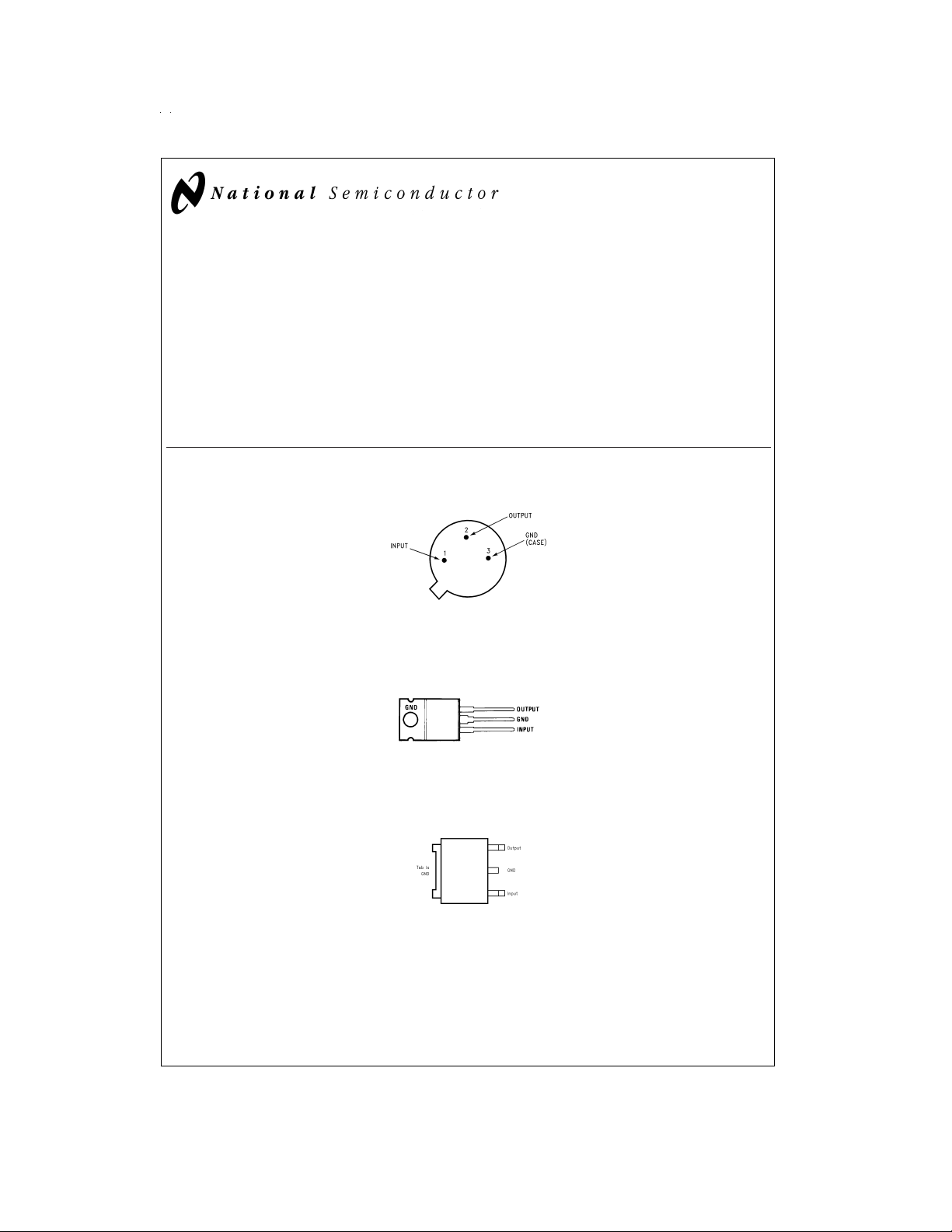
Connection Diagrams
TO-39 Metal Can Package (H)
DS010484-5
Bottom View
Order Number LM78M05CH, LM78M12CH or LM78M15CH
See NS Package Number H03A
TO-220 Power Package (T)
DS010484-6
Top View
Order Number LM341T-5.0, LM341T-12, LM341T-15, LM78M05CT, LM78M12CT or LM78M15CT
See NS Package Number T03B
TO-252
DS010484-19
Top View
Order Number LM78M05CDT
See NS Package Number TD03B
July 1999
LM341/LM78MXX Series 3-Terminal Positive Voltage Regulators
© 1999 National Semiconductor Corporation DS010484 www.national.com
Absolute Maximum Ratings (Note 1)
If Military/Aerospace specified devices are required,
please contact the National Semiconductor Sales Office/
Distributors for availability and specifications.
Lead Temperature (Soldering, 10 seconds)
TO-39 Package (H) 300˚C
TO-220 Package (T) 260˚C
Storage Temperature Range −65˚C to +150˚C
Operating Junction Temperature
Range −40˚C to +125˚C
Power Dissipation (Note 2) Internally Limited
Input Voltage
5V ≤ V
O
≤ 15V 35V
ESD Susceptibility TBD
Electrical Characteristics
Limits in standard typeface are for T
J
=
25˚C, and limits in boldface type apply over the −40˚C to +125˚C operating temperature
range. Limits are guaranteed by production testing or correlation techniques using standard Statistical Quality Control (SQC)
methods.
LM341-5.0, LM78M05C
Unless otherwise specified: V
IN
=
10V, C
IN
=
0.33 µF, C
O
=
0.1 µF
Symbol Parameter Conditions Min Typ Max Units
V
O
Output Voltage I
L
=
500 mA 4.8 5.0 5.2 V
5mA≤I
L
≤500 mA 4.75 5.0 5.25
P
D
≤ 7.5W, 7.5V ≤ V
IN
≤ 20V
V
R LINE
Line Regulation 7.2V ≤ V
IN
≤ 25V I
L
=
100 mA 50 mV
I
L
=
500 mA 100
V
R LOAD
Load Regulation 5 mA ≤ I
L
≤ 500 mA 100
I
Q
Quiescent Current I
L
=
500 mA 4 10.0 mA
∆I
Q
Quiescent Current Change 5 mA ≤ I
L
≤ 500 mA 0.5
7.5V ≤ V
IN
≤ 25V, I
L
=
500 mA 1.0
V
n
Output Noise Voltage f
=
10 Hz to 100 kHz 40 µV
Ripple Rejection f
=
120 Hz, I
L
=
500 mA
78 dB
V
IN
Input Voltage Required I
L
=
500 mA 7.2 V
to Maintain Line Regulation
∆V
O
Long Term Stability I
L
=
500 mA 20 mV/khrs
www.national.com 2
Electrical Characteristics
Limits in standard typeface are for T
J
=
25˚C, and limits in boldface type apply over the −40˚C to +125˚C operating temperature
range. Limits are guaranteed by production testing or correlation techniques using standard Statistical Quality Control (SQC)
methods. (Continued)
LM341-12, LM78M12C
Unless otherwise specified: V
IN
=
19V, C
IN
=
0.33 µF, C
O
=
0.1 µF
Symbol Parameter Conditions Min Typ Max Units
V
O
Output Voltage I
L
=
500 mA 11.5 12 12.5 V
5mA≤I
L
≤500 mA 11.4 12 12.6
P
D
≤ 7.5W, 14.8V ≤ V
IN
≤ 27V
V
R LINE
Line Regulation 14.5V ≤ V
IN
≤ 30V I
L
=
100 mA 120 mV
I
L
=
500 mA 240
V
R LOAD
Load Regulation 5 mA ≤ I
L
≤ 500 mA 240
I
Q
Quiescent Current I
L
=
500 mA 4 10.0 mA
∆I
Q
Quiescent Current Change 5 mA ≤ I
L
≤ 500 mA 0.5
14.8V ≤ V
IN
≤ 30V, I
L
=
500 mA 1.0
V
n
Output Noise Voltage f
=
10 Hz to 100 kHz 75 µV
Ripple Rejection f
=
120 Hz, I
L
=
500 mA
71 dB
V
IN
Input Voltage Required I
L
=
500 mA 14.5 V
to Maintain Line Regulation
∆V
O
Long Term Stability I
L
=
500 mA 48 mV/khrs
LM341-15, LM78M15C
Unless otherwise specified: V
IN
=
23V, C
IN
=
0.33 µF, C
O
=
0.1 µF
Symbol Parameter Conditions Min Typ Max Units
V
O
Output Voltage I
L
=
500 mA 14.4 15 15.6 V
5mA≤I
L
≤500 mA 14.25 15 15.75
P
D
≤ 7.5W, 18V ≤ V
IN
≤ 30V
V
R LINE
Line Regulation 17.6V ≤ V
IN
≤ 30V I
L
=
100 mA 150 mV
I
L
=
500 mA 300
V
R LOAD
Load Regulation 5 mA ≤ I
L
≤ 500 mA 300
I
Q
Quiescent Current I
L
=
500 mA 4 10.0 mA
∆I
Q
Quiescent Current Change 5 mA ≤ I
L
≤ 500 mA 0.5
18V ≤ V
IN
≤ 30V, I
L
=
500 mA 1.0
V
n
Output Noise Voltage f
=
10 Hz to 100 kHz 90 µV
Ripple Rejection f
=
120 Hz, I
L
=
500 mA
69 dB
V
IN
Input Voltage Required I
L
=
500 mA 17.6 V
to Maintain Line Regulation
∆V
O
Long Term Stability I
L
=
500 mA 60 mV/khrs
Note 1: Absolute maximum ratings indicate limits beyond which damage to the component may occur. Electrical specificationsdonotapplywhenoperating the de-
vice outside of its rated operating conditions.
Note 2: The typical thermal resistance of the three package types is:
T (TO-220) package: θ
(JA)
=
60 ˚C/W, θ
(JC)
=
5 ˚C/W
H (TO-39) package: θ
(JA)
=
120 ˚C/W, θ
(JC)
=
18 ˚C/W
DT (TO-252) package: θ
(JA)
=
92 ˚C/W, θ
(JC)
=
10 ˚C/W
www.national.com3
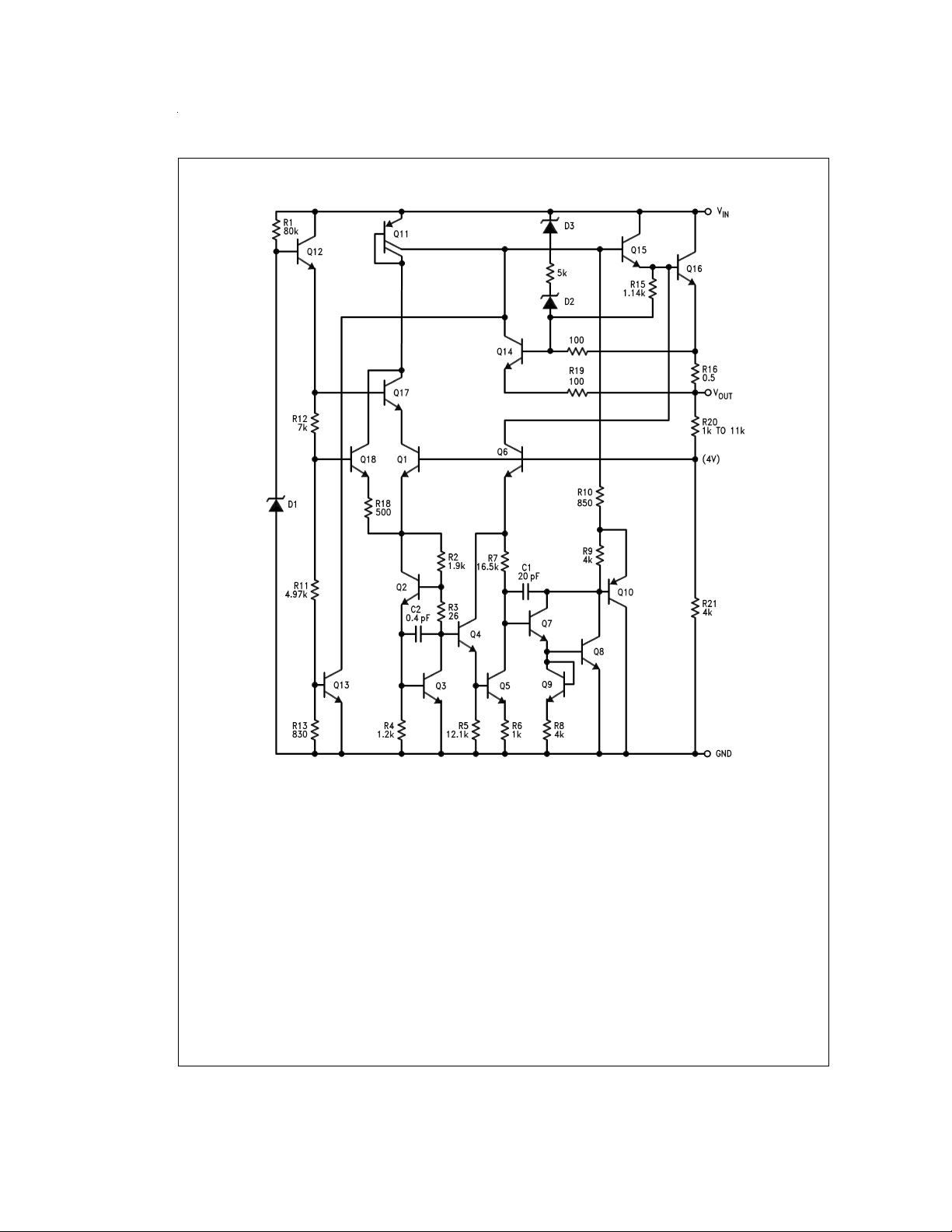
Schematic Diagram
DS010484-1
www.national.com 4
 Loading...