


LMH6672MRX
NSC LMH6672MRX, LMH6672MR, LMH6672MDC, LMH6672MAX, LMH6672MA Datasheet
...
LMH6672
Dual, High Output Current, High Speed Op Amp
General Description
The LMH6672 is a low cost, dual high speed op amp capable
of driving signals to within 1V of the power supply rails. It
features the highoutput drive with low distortion required for
the demanding application of a single supply xDSL line
driver.
When connected as a differential output driver,theLMH6672
can drive a 50Ω load to 16.8V
PP
swing with only −93dBc
distortion, fully supporting the peak upstream power levels
for upstream full-rate ADSL. The LMH6672 is fully specified
for operation with 5V and 12V supplies. Ideal for PCI modem
cards and xDSL modems.
Applications
n ADSL PCI modem cards
n xDSL external modems
n Line drivers
Features
n High Output Drive
19.2V
PP
differential output voltage, RL=50Ω
9.6V
PP
single-ended output voltage, RL=25Ω
n High Output Current
±
200mA@VO=9
VPP,VS
= 12V
n Low Distortion
93dB SFDR
@
100KHz, VO= 8.4VPP,RL=25Ω
92dB SFDR
@
1MHz, VO=2VPP,RL= 100Ω
n High Speed
130MHz 3dB bandwidth (G = 2)
160V/µs slew rate
n Low Noise
4.5nV/
: input noise voltage
1.7pA/
: input noise current
n Low supply current: 6.2mA/amp
n Single-supply operation: 5V to 12V
n Available in 8-pin SOIC, PSOP and LLP
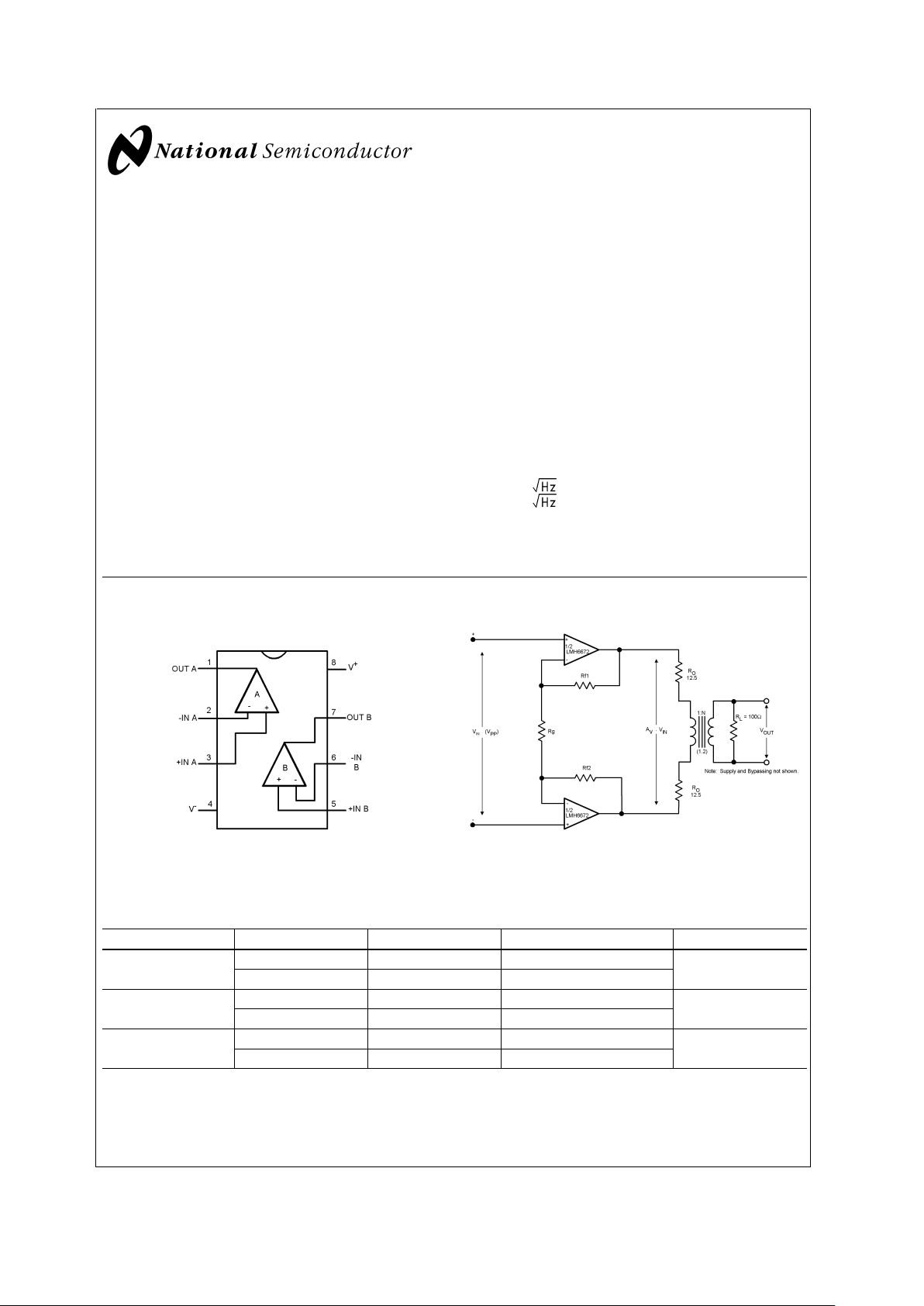
Connection Diagram
8-Pin SOIC/PSOP/LLP
20016602
Top View
Typical Application
20016601
Figure 1
Ordering Information
Package Part Number Package Marking Transport Media NSC Drawing
8-Pin SOIC LMH6672MA LMH6672MA Rails M08A
LMH6672MAX LMH6672MA 2.5k Units Tape and Reel
8-Pin PSOP LMH6672MR LMH6672MR Rails MRA08A
LMH6672MRX LMH6672MR 2.5k Units Tape and Reel
8-Pin LLP LMH6672LD L6672LD 1k Units Tape and Reel LDC08A
LMH6672LDX L6672LD 4.5k Units Tape and Reel
January 2002
LMH6672 Dual, High Output Current, High Speed Op Amp
© 2002 National Semiconductor Corporation DS200166 www.national.com
Absolute Maximum Ratings (Note 1)
If Military/Aerospace specified devices are required,
please contact the National Semiconductor Sales Office/
Distributors for availability and specifications.
ESD Tolerance (Note 2)
Human Body Model 2kV
Machine Model 200V
V
IN
Differential
±
1.2V
Output Short Circuit Duration (Note 2)
Supply Voltage (V
+−V−
) 13.2V
Voltage at Input/Output pins V
+
+0.8V, V−−0.8V
Storage Temperature Range −65˚C to +150˚C
Junction Temperature +150˚C (Note 4)
Soldering Information
Infrared or Convection (20 sec) 235˚C
Wave Soldering (10 sec) 260˚C
Operating Ratings (Note 1)
Supply Voltage (V
+-V−
)
±
2.5V to±6.5V
Junction Temperature Range −40˚C to 150˚C
Package Thermal Resistance (θ
JA
)
8-pin SOIC 172˚C/W
8-pin PSOP 58.6˚C/W
8-pin LLP 40˚C/W
Electrical Characteristics
TJ= 25˚C, G = +2, VS=±2.5 to±6V, Rf=RIN= 470Ω,RL= 100Ω; Unless otherwise specified.
Symbol Parameter Conditions Min
(Note 6)
Typ
(Note 5)
Max
(Note 6)
Units
Dynamic Performance
−3dB Bandwidth 130 MHz
0.1dB Bandwidth V
S
=±6V 22 MHz
Slew Rate V
S
=±6V, 4V Step, 10-90% 170 V/µs
Rise and Fall Time V
S
= 6V, 4V Step, 10-90% 18.5 ns
Distortion and Noise Response
2
nd
Harmonic Distortion VO= 8.4VPP, f = 100KHz, RL=25Ω −95 dBc
V
O
= 8.4VPP, f = 1MHz, RL= 100Ω −92 dBc
3
rd
Harmonic Distortion VO= 8.4VPP, f = 100KHz, RL=25Ω −93 dBc
V
O
=2VPP, f = 1MHz, RL= 100Ω −95 dBc
Input Noise Voltage f = 100KHz 4.5 nV
Input Noise Current f = 100KHz 1.7 pA/
Input Characteristics
V
OS
Input Offset Voltage TJ= −40˚C to 150˚C −5.5 −0.2 5.5
mV
−4 −0.2 4
I
B
Input Bias Current TJ= −40˚C to 150˚C 8 14 µA
I
OS
Input Offset Current TJ= −40˚C to 150˚C −2.1 0 2.1 µA
CMVR Common Voltage Range V
S
=±6V −6.0 4.5 V
CMRR Common-Mode Rejection Ratio V
S
=±6V, TJ= −40˚C to 150˚C 150 9.5 µV/V
Transfer Characteristics
A
VOL
Voltage Gain RL= 1k, TJ= −40˚C to 150˚C 1.0 2.5 V/mV
R
L
=25Ω,TJ= −40˚C to 150˚C 0.67 1.7 V/mV
Output Swing R
L
=25Ω,VS=±6V −4.5
±
4.8 4.5
V
R
L
=25Ω,TJ= −40˚C to 150˚C,
V
S
=±6V
−4.4
±
4.8 4.4
Output Swing R
L
= 1k, VS=±6V −4.8
±
4.8 4.8
V
R
L
= 1k, TJ= −40˚C to 150˚C,
V
S
=±6V
−4.7
±
4.8 4.7
I
SC
Output Current (Note 3) VO=0,VS=±6V 400 788 mA
V
O
=0,VS=±6V,
T
J
= −40˚C to 150˚C
260 600 mA
Power Supply
LMH6672
www.national.com 2
Electrical Characteristics (Continued)
TJ= 25˚C, G = +2, VS=±2.5 to±6V, Rf=RIN= 470Ω,RL= 100Ω; Unless otherwise specified.
Symbol Parameter Conditions Min
(Note 6)
Typ
(Note 5)
Max
(Note 6)
Units
I
S
Supply Current/Amp VS=±6V 8
mA
V
S
=±6V, TJ= −40˚C to 150˚C 6.2 9
PSRR Power Supply Rejection Ratio V
S
=±2.5V to±6V,
T
J
= −40˚C to 150˚C
72 78 dB
±
2.5V Electrical Characteristics
TJ= 25˚C, G = +2, VS=±2.5 to±6V, Rf=RIN= 470Ω,RL= 100Ω; Unless otherwise specified.
Symbol Parameter Conditions Min
(Note 6)
Typ
(Note 5)
Max
(Note 6)
Units
Dynamic Performance
−3dB Bandwidth 125 MHz
0.1dB Bandwidth 32 MHz
Slew Rate 0.4V Step, 10-90% 115 V/µs
Rise and Fall Time 0.4V Step, 10-90% 2.75 ns
Distortion and Noise Response
2
nd
Harmonic Distortion VO=2VPP, f = 100KHz, RL=25Ω −85 dBc
V
O
=2VPP, f = 1MHz, RL= 100Ω −87 dBc
3
rd
Harmonic Distortion VO=2VPP, f = 100KHz, RL=25Ω −90 dBc
V
O
=2VPP, f = 1MHz, RL= 100Ω −88 dBc
Input Characteristics
V
OS
Input Offset Voltage TJ= −40˚C to 150˚C −5.5 5.5
mV
−4.0 1.1 4.0
I
B
Input Bias Current TJ= −40˚C to 150˚C 8.0 14 µA
CMVR Common-Mode Voltage Range −2.5 1.0 V
CMRR Common-Mode Rejection Ratio T
J
= −40˚C to 150˚C 150 57 µV/V
Transfer Characteristics
A
VOL
Voltage Gain RL=25Ω,TJ= −40˚C to 150˚C 0.67 1.54
V/mV
R
L
= 1k, TJ= −40˚C to 150˚C 1.0 2.0
Output Characteristics
V
O
Output Voltage Swing RL=25Ω 1.20 1.45
VR
L
=25Ω,TJ= −40˚C to 150˚C 1.10 1.35
R
L
= 1k 1.30 1.60
R
L
= 1k, TJ= −40˚C to 150˚C 1.25 1.50
Power Supply
I
S
Supply Current/Amp 8.0
mA
T
J
= −40˚C to 150˚C 5.6 9.0
Note 1: Absolute Maximum Ratings indicate limits beyond which damage to the device may occur. Operating Ratings indicate conditions for which the device is
intended to be functional, but specific performance is not guaranteed. For guaranteed specifications and the test conditions, see the Electrical Characteristics.
Note 2: Human body model, 1.5kΩ in series with 100pF. Machine model, 200Ω in series with 100pF.
Note 3: Shorting the output to either supply or ground will exceed the absolute maximum T
J
and can result in failure.
Note 4: The maximum power dissipation is a function of T
J(MAX)
, θJAand TA. The maximum allowable power dissipation at any ambient temperature is PD=
(T
J(MAX)−TA
)/θJA. All numbers apply for packages soldered directly onto a PC board.
Note 5: Typical values represent the most likely parametric norm.
Note 6: All limits are guaranteed by testing, characterization or statistical analysis.
LMH6672
www.national.com3
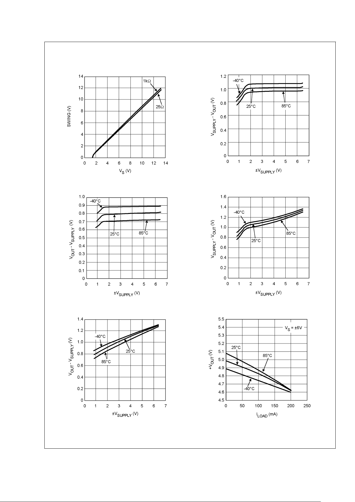
Typical Performance Characteristics At T
J
= 25˚C, RF= 470Ω gain = +2, RL= 100Ω. Unless oth-
erwise specified.
Output Swing R
L
=25Ω,1kΩ@−40˚C, 25˚C, 85˚C Positive Output Swing into 1kΩ
20016635 20016645
Negative Output Swing into 1kΩ Positive Output Swing into 25Ω
20016646
20016644
Negative Output Swing into 25Ω +V
OUT
vs. I
LOAD
20016647 20016640
LMH6672
www.national.com 4
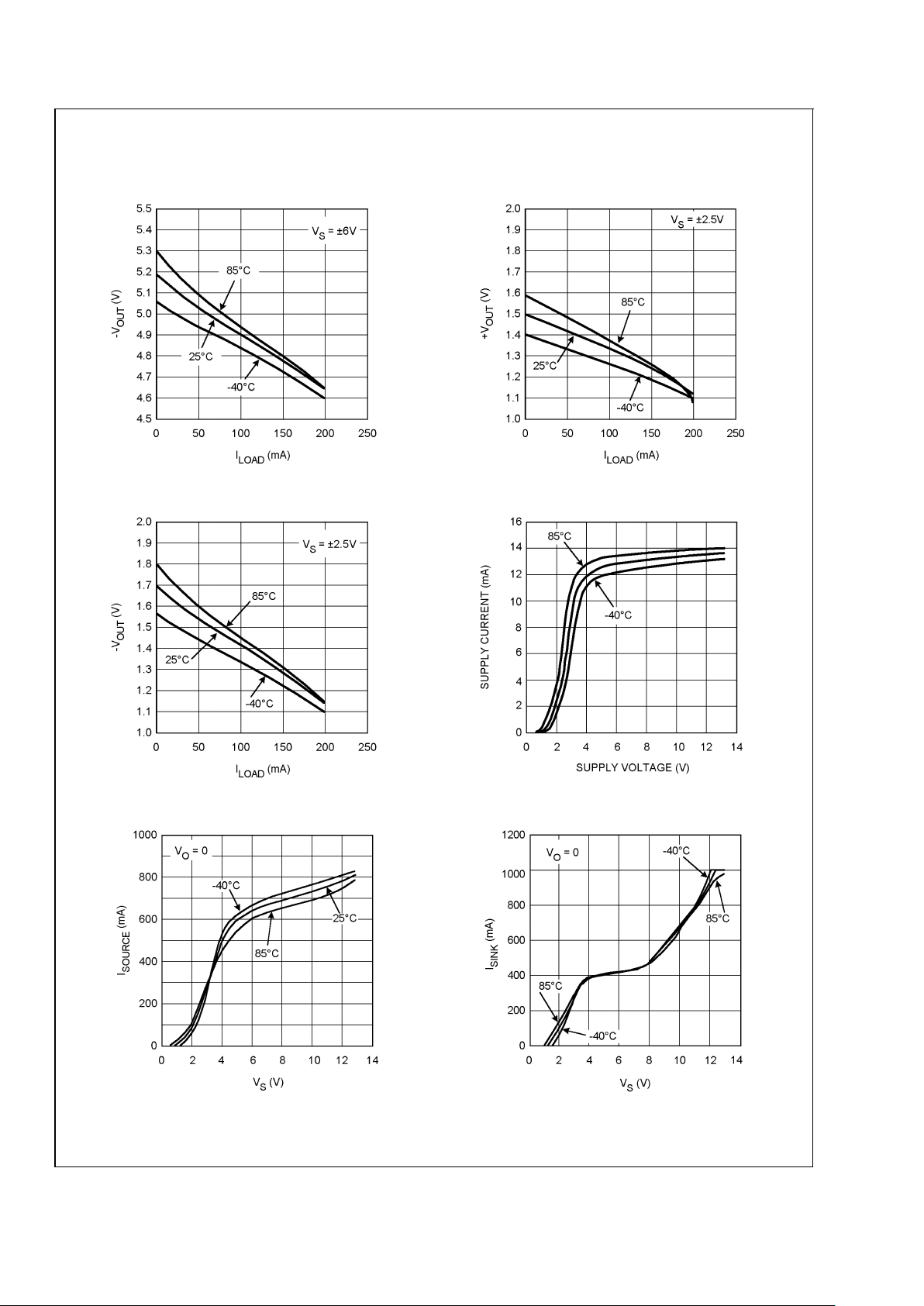
Typical Performance Characteristics At T
J
= 25˚C, RF= 470Ω gain = +2, RL= 100Ω. Unless
otherwise specified. (Continued)
−V
OUT
vs. I
LOAD
+V
OUT
vs. I
LOAD
20016641 20016643
−V
OUT
vs. I
LOAD
Supply Current vs. Supply Voltage
20016642
20016632
Sourcing Current vs. Supply Voltage Sinking Current vs. Supply Voltage
20016633 20016634
LMH6672
www.national.com5
 Loading...