


LMC6584BIMX
NSC LMC6584BIMX, LMC6584BIM, LMC6584AIM, LMC6582BIN, LMC6582BIMX Datasheet
...
LMC6582 Dual/LMC6584 Quad
Low Voltage, Rail-To-Rail Input and Output CMOS
Operational Amplifier
May 1995
LMC6582 Dual/LMC6584 Quad Low Voltage, Rail-To-Rail Input and Output CMOS Operational
Amplifier
General Description
The LMC6582/4 is a high performance operational amplifier
which can operateover a wide range of supply voltages with
guaranteed specifications at 1.8V, 2.2V, 3V, 5V, and 10V.
The LMC6582/4 provides an input common-mode voltage
range that exceeds both supplies. The rail-to-rail output
swing of the amplifier assures maximum dynamic signal
range. This rail-to-rail performance of the amplifier, combined with its high open-loop voltage gain makes it unique
among rail-to-rail CMOS amplifiers. The LMC6582/4 is an
excellent choice for circuits where the input common-mode
voltage range is a concern.
The LMC6582/4 has been designed specifically to improve
system performance in low voltage applications. Guaranteed
operation down to 1.8V means that this family of amplifiers
can operate at the end of discharge (EOD) voltages of several popular batteries. The amplifier’s 80 fA input current, 0.5
mV offset voltage, and 82 dB CMRR maintain accuracy in
battery-powered systems.
For a single, dual or quad CMOS amplifier with similar specs
and a powerdown mode, refer to the LMC6681/2/4
datasheet.
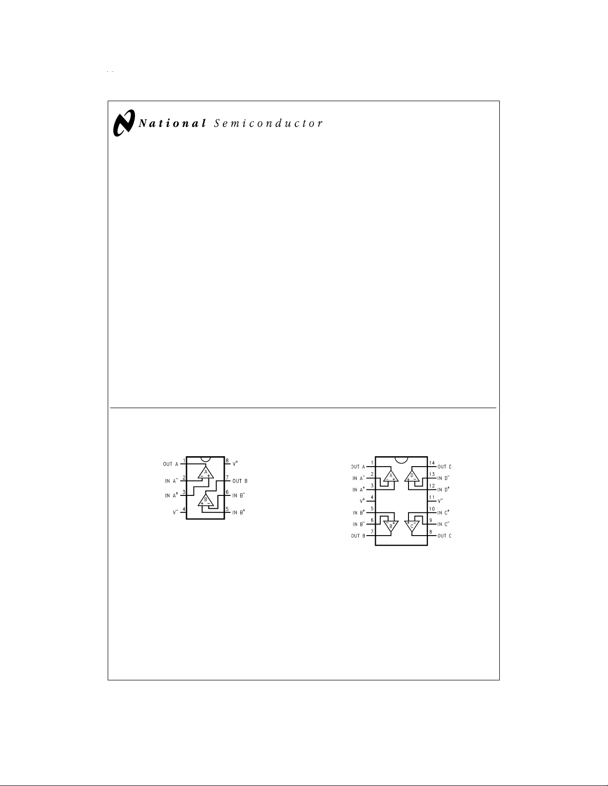
Connection Diagrams
8-Pin DIP/SO
Features
(Typical unless otherwise noted)
n Guaranteed Specs at 1.8V, 2.2V, 3V, 5V, 10V
n Rail-to-Rail Input Common-Mode Voltage Range
n Rail-to-Rail Output Swing
(within 10 mV of supply rail,
n CMRR and PSRR: 82 dB
n Ultra Low Input Current: 80 fA
n High Voltage Gain (V
n Unity Gain Bandwidth: 1.2 MHz
=
S
@
3V, R
=
V
3V and R
S
=
10 kΩ): 120 dB
L
Applications
n Battery Operated Systems
n Sensor Amplifiers
n Portable Communication Devices
n Medical Instrumentation
n Level Detectors, Sample-and-Hold Circuits
n Battery Monitoring
14-Pin DIP/SO
L
=
10 kΩ)
DS012041-1
Top View
DS012041-2
Top View
© 1999 National Semiconductor Corporation DS012041 www.national.com
Ordering Information
Package Temperature Range NSC Transport
8-pin Molded DIP LMC6582AIN, LMC6582BIN N08E Rails
8-pin Small Outline LMC6582AIM, LMC6582BIM M08A Rails
14-pin Molded DIP LMC6584AIN, LMC6584BIN N14A Rails
14-pin Small Outline LMC6584AIM, LMC6584BIM M14A Rails
Industrial, −40˚C to +85˚C Drawing Media
LMC6582AIMX, LMC6582BIMX M08A Tape and Reel
LMC6584AIMX, LMC6584BIMX M14A Tape and Reel
www.national.com 2
Absolute Maximum Ratings (Note 1)
If Military/Aerospace specified devices are required,
please contact the National Semiconductor Sales Office/
Distributors for availability and specifications.
ESD Tolerance (Note 2) 2 kV
Differential Input Voltage
Voltage at Input/Output Pin (V
Supply Voltage (V
+−V−
) 12V
Current at Input Pin (Note 11)
Current at Output Pin (Note 3)
Current at Power Supply Pin 35 mA
Lead Temp. (soldering, 10 sec.) 260˚C
Storage Temperature Range −65˚C to +150˚C
±
Supply Voltage
+
) +0.3V, (V−) −0.3V
±
5mA
±
30 mA
Junction Temperature (Note 4) 150˚C
Operating Ratings (Note 1)
Supply Voltage 1.8V ≤ V
Junction Temperature Range
LMC6582AI, LMC6582BI −40˚C ≤ T
LMC6584AI, LMC6584BI −40˚C ≤ T
Thermal Resistance (θ
)
JA
N Package, 8-pin Molded DIP 108˚C/W
M Package, 8-pin Surface Mount 172˚C/W
N Package, 14-pin Molded DIP 88˚C/W
M Package, 14-pin Surface Mount 126˚C/W
≤ 10V
S
≤ +85˚C
J
≤ +85˚C
J
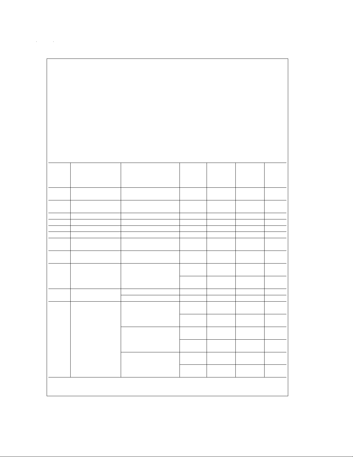
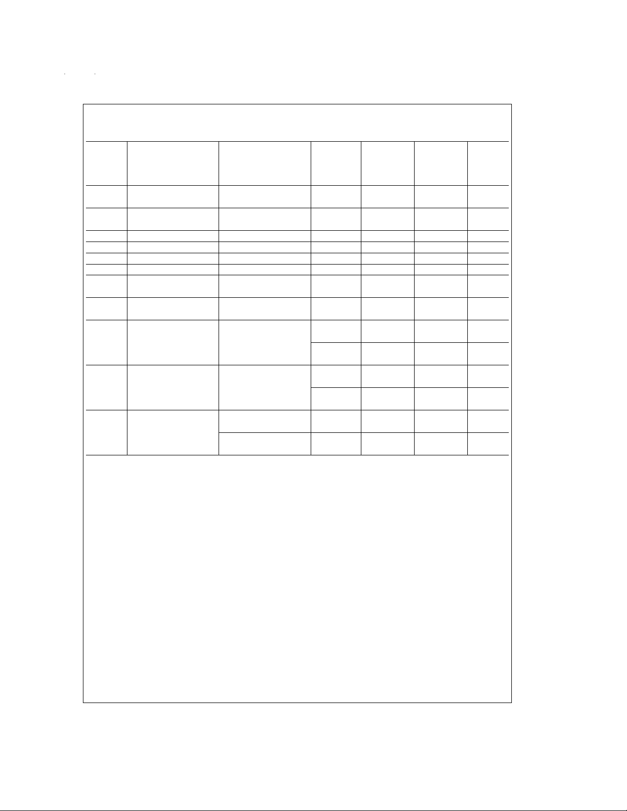
3V DC Electrical Characteristics
Unless otherwise specified, all limits guaranteed for T
face limits apply at the temperature extremes.
=
J
25˚C, V
+
=
3.0V, V
−
=
0V, V
CM
+
=
=
/2 and R
V
V
O
>
1MΩ.Bold-
L
LMC6582AI LMC6582BI
Symbol Parameter Conditions Typ LMC6584AI LMC6584BI Units
(Note 5) Limit Limit
(Note 6) (Note 6)
V
OS
Input Offset Voltage 0.5 1 3 mV
2.5 4.5 max
TCV
Input Offset Voltage 1.5 µV/˚C
OS
Average Drift
I
B
I
OS
R
IN
C
IN
Input Current (Note 12) 0.08 20 20 pA max
Input Offset Current (Note 12) 0.04 10 10 pA max
Input Resistance
>
1 Tera Ω
Input Capacitance 3 pF
CMRR Common Mode (Note 13) 82 70 65 dB
Rejection Ratio 65 62 min
PSRR Power Supply
Rejection Ratio V
V
CM
Input Common Mode CMRR>50 dB 3.23 3.18 3.18 V
±
1.5V ≤ VS≤±2.5V 82 70 65 dB
+
=
/2=V
V
O
CM
65 62 min
Voltage Range 3.00 3.00 min
−0.3 −0.18 −0.18 V
0.00 0.00 max
A
V
V
O
Large Signal
Voltage Gain
Output Swing R
=
R
600Ω (Notes 7, 12) 70 10 10 V/mV
L
=
R
10 kΩ (Notes 7, 12) 1000 12 12 V/mV
L
=
L
600Ω to V
+
/2 2.87 2.70 2.70 V
2.58 2.58 min
0.15 0.3 0.3 V
0.42 0.42 max
R
L
=
2kΩto V
+
/2 2.95 2.85 2.85 V
2.79 2.79 min
0.05 0.15 0.15 V
0.21 0.21 max
R
L
=
10 kΩ to V
+
/2 2.99 2.94 2.94 V
2.91 2.91 min
0.01 0.04 0.04 V
0.05 0.05 max
www.national.com3
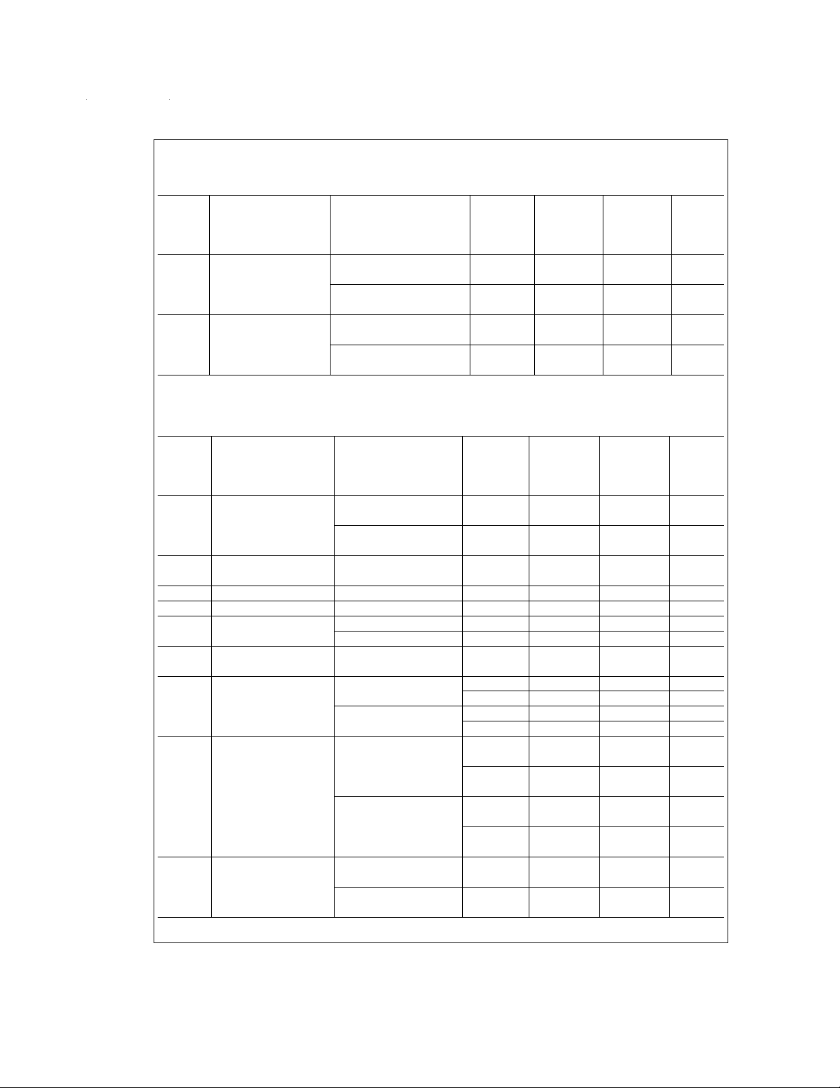
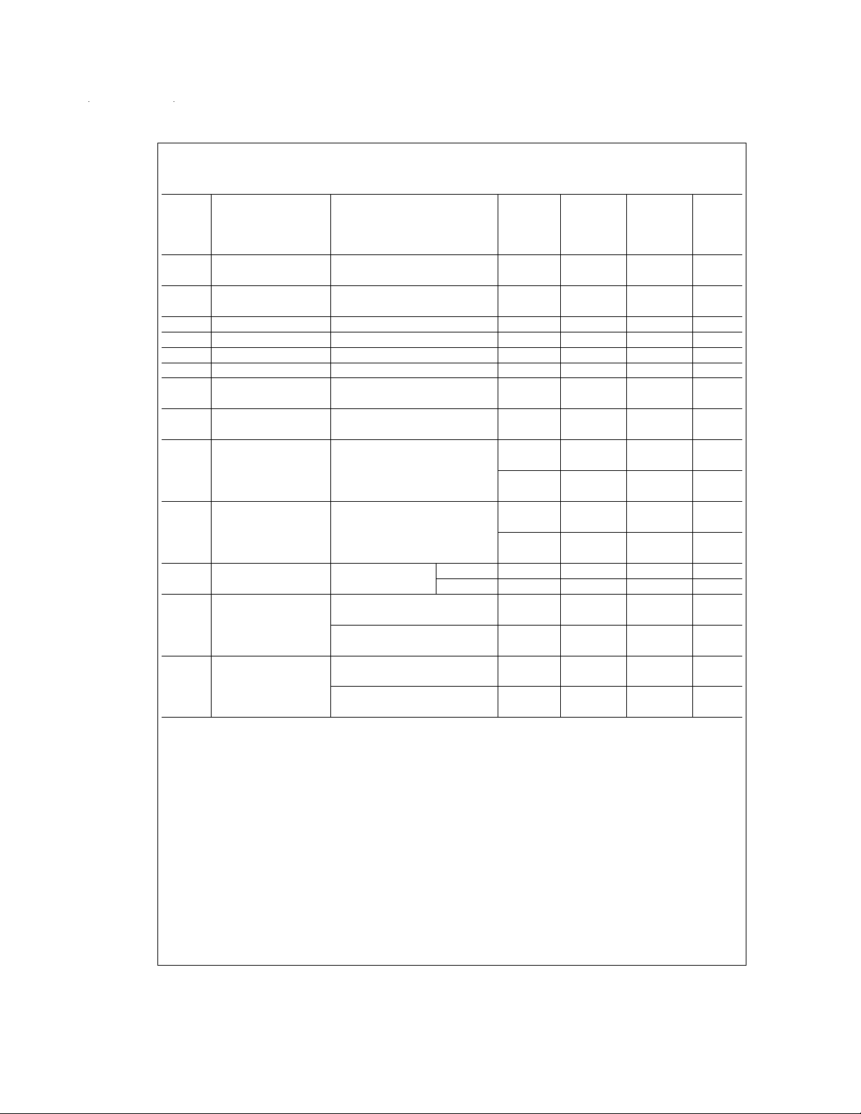
3V DC Electrical Characteristics (Continued)
Unless otherwise specified, all limits guaranteed for T
face limits apply at the temperature extremes.
=
J
25˚C, V
+
=
Symbol Parameter Conditions Typ LMC6584AI LMC6584BI Units
I
SC
Output Short Circuit Sourcing, V
=
0V 20 9.0 9.0 mA
O
Current 6.7 6.7 min
Sinking, V
I
S
Supply Current Dual, LMC6582 1.4 2.26 2.26 mA
V
CM
=
3V 12 6.0 6.0 mA
O
=
1.5V 2.75 2.75 max
Quad, LMC6584 2.8 4.52 4.52 mA
=
V
1.5V 5.42 5.42 max
CM
3.0V, V
−
=
0V, V
CM
+
=
=
/2 and R
V
V
O
LMC6582AI LMC6582BI
(Note 5) Limit Limit
(Note 6) (Note 6)
4.5 4.5 min
>
1MΩ.Bold-
L
1.8V and 2.2V DC Electrical Characteristics
Unless otherwise specified, all limits guaranteed for T
Ω. Boldface limits apply at the temperature extremes.
=
J
25˚C, V
+
=
1.8V and 2.2V, V
−
=
0V, V
CM
+
=
=
/2 and R
V
V
O
>
L
LMC6582AI LMC6582BI
Symbol Parameter Conditions Typ LMC6584AI LMC6584BI Units
(Note 5) Limit Limit
(Note 6) (Note 6)
+
V
OS
Input Offset Voltage V
=
1.8V, V
=
1.5V 0.5 3 10 mV
CM
max
+
=
V
2.2V, V
=
1.5V 0.5 2 6 mV
CM
3.8 7.8 max
+
TCV
Input Offset Voltage V
os
=
2.2V 1.5 µV/˚C
Average Drift
+
I
B
I
OS
Input Current V
Input Offset Current V
CMRR Common Mode V
Rejection Ratio V
PSRR Power Supply
Rejection Ratio V
V
CM
Input Common Mode V
Voltage Range −0.15 0.0 0.0 V max
V
O
Output Swing V
=
2.2V (Note 12) 0.08 20 20 pA max
+
=
2.2V (Note 12) 0.04 10 10 pA max
+
=
2.2V, (Note 13) 82 60 60 dB min
+
=
1.8V, (Note 13) 82 50 50 dB min
±
1.1V ≤ VS≤±5V, 82 70 65 dB
+
=
/2=V
V
O
+
=
CMRR
+
=
V
CMRR
+
=
=
R
L
2.2V
>
1.8V
>
CM
40 dB
40 dB
2.38 2.2 2.2 V min
1.98 1.8 1.8 V min
−0.10 0.0 0.0 V max
2.2V 2.15 2.0 2.0 V
+
2kΩto V
/2 1.88 1.88 min
65 62 min
0.05 0.2 0.2 V
0.32 0.32 max
+
=
V
1.8V 1.75 1.6 1.6 V
=
R
2kΩto V
L
+
/2 1.44 1.44 min
0.05 0.2 0.2 V
0.36 0.36 max
I
S
Supply Current Dual, LMC6582 1.4 2.2 2.2 mA
=
V
1.5V 2.7 2.7 max
CM
Quad, LMC6584 2.8 4.4 4.4 mA
=
V
1.5V 5.3 5.3 max
CM
1M
www.national.com 4
5V DC Electrical Characteristics
Unless otherwise specified, all limits guaranteed for T
face limits apply at the temperature extremes.
=
J
25˚C, V
+
=
5.0V, V
−
=
0V, V
CM
+
=
=
/2 and R
V
V
O
>
1MΩ.Bold-
L
LMC6582AI LMC6582BI
Symbol Parameter Conditions Typ LMC6584AI LMC6584BI Units
(Note 5) Limit Limit
(Note 6) (Note 6)
V
OS
Input Offset Voltage V
=
1.5V 0.5 1 3 mV
CM
2.5 4.5 max
TCV
Input Offset Voltage 1.5 µV/˚C
OS
Average Drift
I
B
I
OS
R
IN
C
IN
Input Current (Note 12) 0.08 20 20 pA max
Input Offset Current (Note 12) 0.04 10 10 pA max
Input Resistance
>
1 Tera Ω
Input Capacitance 3 pF
CMRR Common Mode (Note 13) 82 70 65 dB
Rejection Ratio 65 62 min
PSRR Power Supply
Rejection Ratio V
V
CM
Input Common Mode CMRR>50 dB 5.3 5.18 5.18 V
±
1.5V ≤ VS≤±2.5V, 82 70 65 dB
+
=
/2=V
V
O
CM
65 62 min
Voltage Range 5.00 5.00 min
−0.3 −0.18 −0.18 V
0.00 0.00 max
V
O
Output Swing R
=
L
2kΩto V
+
/2 4.9 4.85 4.85 V
4.58 4.58 min
0.05 0.2 0.2 V
0.28 0.28 max
I
S
Supply Current Dual, LMC6582 1.5 2.48 2.48 mA
=
V
1.5V 3.00 3.00 max
CM
Quad, LMC6584 3.0 4.96 4.96 mA
=
V
1.5V 6.00 6.00 max
CM
www.national.com5
10V DC Electrical Characteristics
Unless otherwise specified, all limits guaranteed for T
Boldface limits apply at the temperature extremes.
=
J
25˚C, V
+
=
10.0V, V
−
=
0V, V
=
CM
+
=
/2 and R
V
V
O
L
>
1MΩ.
LMC6582AI LMC6582BI
Symbol Parameter Conditions Typ LMC6584AI LMC6584BI Units
(Note 5) Limit Limit
(Note 6) (Note 6)
V
OS
Input Offset Voltage V
=
1.5V 0.5 1.5 3.5 mV
CM
3.0 5.0 max
TCV
Input Offset Voltage 1.5 µV/˚C
OS
Average Drift
I
B
I
OS
R
IN
C
IN
Input Current (Note 12) 0.08 20 20 pA max
Input Offset Current (Note 12) 0.04 10 10 pA max
Input Resistance
>
1 Tera Ω
Input Capacitance 3 pF
CMRR Common Mode (Note 13) 82 65 65 dB
Rejection Ratio 62 62 min
PSRR Power Supply
Rejection Ratio V
V
CM
Input Common Mode CMRR>50 dB 10.30 10.18 10.18 V
±
1.1V ≤ V+≤±5V, 82 70 65 dB
+
=
/2=V
V
O
CM
65 62 min
Voltage Range 10.00 10.00 min
−0.30 −0.18 −0.18 V
0.00 0.00 max
V
O
Output Swing R
=
L
2kΩto V
+
/2 9.93 9.7 9.7 V
9.58 9.58 min
0.08 0.3 0.3 V
0.42 0.42 max
A
V
Large Signal R
=
L
2kΩto V
+
/2 Sourcing 89 25 25 V/mV
Voltage Gain (Note 12) Sinking 224 25 25 V/mV
I
SC
Output Short Circuit Sourcing, V
=
0V 65 30 30 mA
O
Current (Note 14) 22 22 min
Sinking, V
=
10V 70 30 30 mA
O
(Note 14) 22 22 min
I
S
Supply Current Dual, LMC6582 1.6 3.0 3.0 mA
=
V
1.5V 3.6 3.6 max
CM
Quad, LMC6584 3.2 6.0 6.0 mA
=
V
1.5V 7.2 7.2 max
CM
www.national.com 6
 Loading...