


NSC LMC6482IN, LMC6482IMX, LMC6482IMMX, LMC6482AIN, LMC6482AIMX Datasheet
...
November 1997
LMC6482
CMOS Dual Rail-To-Rail Input and Output Operational
Amplifier
General Description
The LMC6482 provides a common-mode range that extends to both supply rails. This rail-to-rail performance combined with excellent accuracy, due to a high CMRR, makes it unique among rail-to-rail input amplifiers.
It is ideal for systems, such as data acquisition, that require a large input signal range. The LMC6482 is also an excellent upgrade for circuits using limited common-mode range amplifiers such as the TLC272 and TLC277.
Maximum dynamic signal range is assured in low voltage and single supply systems by the LMC6482's rail-to-rail output swing. The LMC6482's rail-to-rail output swing is guaranteed for loads down to 600Ω.
Guaranteed low voltage characteristics and low power dissipation make the LMC6482 especially well-suited for battery-operated systems.
LMC6482 is also available in MSOP package which is almost half the size of a SO-8 device.
See the LMC6484 data sheet for a Quad CMOS operational amplifier with these same features.
Features
(Typical unless otherwise noted)
nRail-to-Rail Input Common-Mode Voltage Range (Guaranteed Over Temperature)
nRail-to-Rail Output Swing (within 20 mV of supply rail, 100 kΩ load)
nGuaranteed 3V, 5V and 15V Performance
nExcellent CMRR and PSRR: 82 dB
nUltra Low Input Current: 20 fA
nHigh Voltage Gain (RL = 500 kΩ): 130 dB
nSpecified for 2 kΩ and 600Ω loads
nAvailable in MSOP Package
Applications
nData Acquisition Systems
nTransducer Amplifiers
nHand-held Analytic Instruments
nMedical Instrumentation
nActive Filter, Peak Detector, Sample and Hold, pH Meter, Current Source
nImproved Replacement for TLC272, TLC277
3V Single Supply Buffer Circuit
Rail-To-Rail Input |
Rail-To-Rail Output |
DS011713-2
DS011713-3
DS011713-1
Connection Diagram
DS011713-4
Amplifier Operational Output and Input Rail-To-Rail Dual CMOS LMC6482
© 1999 National Semiconductor Corporation |
DS011713 |
www.national.com |

Ordering Information
Package |
Temperature Range |
NSC |
Transport |
Package Marking |
|
|
|
|
Drawing |
Media |
|
|
Military |
Industrial |
|
||
|
−55ÊC to +125ÊC |
−40ÊC to +85ÊC |
|
|
|
|
|
|
|
|
|
8-Pin |
LMC6482MN |
LMC6482AIN, |
N08E |
Rail |
LMC6482MN, |
Molded DIP |
|
LMC6482IN |
|
|
LMC6482AIN, LMC6482IN |
|
|
|
|
|
|
8-pin |
|
LMC6482AIM, |
M08A |
Rail |
LMC6482AIM, LMC6482IM |
Small Outline |
|
LMC6482IM |
|
Tape and Reel |
|
|
|
|
|
|
|
8-pin |
LMC6482AMJ/883 |
|
J08A |
Rail |
LMC6482AMJ/883Q5962-9453401MPA |
Ceramic DIP |
|
|
|
|
|
|
|
|
|
|
|
8-pin |
|
LMC6482IMM |
MUA08A |
Rail |
A10 |
Mini SO |
|
|
|
Tape and Reel |
|
|
|
|
|
|
|
www.national.com |
2 |

Absolute Maximum Ratings (Note 1)
If Military/Aerospace specified devices are required, please contact the National Semiconductor Sales Office/ Distributors for availability and specifications.
ESD Tolerance (Note 2) |
1.5 kV |
Differential Input Voltage |
±Supply Voltage |
Voltage at Input/Output Pin |
(V+) +0.3V, (V− ) −0.3V |
Supply Voltage (V+ − V − ) |
16V |
Current at Input Pin (Note 12) |
±5 mA |
Current at Output Pin |
|
(Notes 3, 8) |
±30 mA |
Current at Power Supply Pin |
40 mA |
Lead Temperature |
|
(Soldering, 10 sec.) |
260ÊC |
Storage Temperature Range |
−65ÊC to +150ÊC |
Junction Temperature (Note 4) |
150ÊC |
Operating Ratings (Note 1)
Supply Voltage |
3.0V £ V+ £ 15.5V |
|
Junction Temperature Range |
|
|
LMC6482AM |
−55ÊC |
£ TJ £ +125ÊC |
LMC6482AI, LMC6482I |
−40ÊC |
£ TJ £ +85ÊC |
Thermal Resistance (qJA) |
|
|
N Package, 8-Pin Molded DIP |
|
90ÊC/W |
M Package, 8-Pin Surface Mount |
|
155ÊC/W |
MSOP package, 8-Pin Mini SO |
|
194ÊC/W |
DC Electrical Characteristics
|
Unless otherwise specified, all limits guaranteed for TJ = 25ÊC, V+ = 5V, V− |
= 0V, VCM = VO = V+/2 and RL > 1M. Boldface |
|||||||||
|
limits apply at the temperature extremes. |
|
|
|
|
|
|
|
|||
Symbol |
Parameter |
Conditions |
Typ |
|
LMC6482AI |
LMC6482I |
LMC6482M |
Units |
|||
|
|
|
|
|
|
(Note 5) |
|
Limit |
Limit |
Limit |
|
|
|
|
|
|
|
|
|
|
|||
|
|
|
|
|
|
|
|
(Note 6) |
(Note 6) |
(Note 6) |
|
|
|
|
|
|
|
|
|
|
|
|
|
|
VOS |
Input Offset Voltage |
|
|
|
0.11 |
|
0.750 |
3.0 |
3.0 |
mV |
|
|
|
|
|
|
|
|
1.35 |
3.7 |
3.8 |
max |
|
|
|
|
|
|
|
|
|
|
|
|
|
TCVOS |
Input Offset Voltage |
|
|
|
1.0 |
|
|
|
|
µV/ÊC |
|
|
Average Drift |
|
|
|
|
|
|
|
|
|
|
|
|
|
|
|
|
|
|
|
|
|
|
IB |
Input Current |
(Note 13) |
|
0.02 |
|
4.0 |
4.0 |
10.0 |
pA |
|
|
|
|
|
|
|
|
|
|
|
|
max |
|
|
|
|
|
|
|
|
|
|
|
|
|
IOS |
Input Offset Current |
(Note 13) |
|
0.01 |
|
2.0 |
2.0 |
5.0 |
pA |
|
|
|
|
|
|
|
|
|
|
|
|
max |
|
|
|
|
|
|
|
|
|
|
|
|
|
CIN |
Common-Mode |
|
|
|
3 |
|
|
|
|
pF |
|
|
Input Capacitance |
|
|
|
|
|
|
|
|
|
|
|
|
|
|
|
|
|
|
|
|
|
|
RIN |
Input Resistance |
|
|
|
>10 |
|
|
|
|
TeraW |
|
CMRR |
Common Mode |
0V £ VCM £ 15.0V |
82 |
|
70 |
65 |
65 |
dB |
||
|
|
Rejection Ratio |
V+ = 15V |
|
|
|
67 |
62 |
60 |
min |
|
|
|
|
0V £ VCM £ 5.0V |
|
82 |
|
70 |
65 |
65 |
|
|
|
|
|
V+ = 5V |
|
|
|
67 |
62 |
60 |
|
|
|
+PSRR |
Positive Power Supply |
5V £ V+ £ 15V, V− = 0V |
82 |
|
70 |
65 |
65 |
dB |
||
|
|
Rejection Ratio |
VO = 2.5V |
|
|
|
67 |
62 |
60 |
min |
|
|
−PSRR |
Negative Power Supply |
−5V £ V− £ −15V, V + = 0V |
82 |
|
70 |
65 |
65 |
dB |
||
|
|
Rejection Ratio |
VO = −2.5V |
|
|
|
67 |
62 |
60 |
min |
|
|
VCM |
Input Common-Mode |
V+ = 5V and 15V |
|
V− − 0.3 |
|
− 0.25 |
− 0.25 |
− 0.25 |
V |
|
|
|
Voltage Range |
For CMRR ³ 50 dB |
|
|
0 |
0 |
0 |
max |
||
|
|
|
|
|
|
|
|
|
|
|
|
|
|
|
|
|
|
V+ + 0.3V |
|
V+ + 0.25 |
V+ + 0.25 |
V+ + 0.25 |
V |
|
|
|
|
|
|
|
|
V+ |
V+ |
V+ |
min |
|
AV |
Large Signal |
RL = 2 kW |
|
Sourcing |
666 |
|
140 |
120 |
120 |
V/mV |
|
|
Voltage Gain |
(Notes 7, 13) |
|
|
|
|
84 |
72 |
60 |
min |
|
|
|
|
|
|
|
|
|
|
|
|
|
|
|
|
|
Sinking |
75 |
|
35 |
35 |
35 |
V/mV |
|
|
|
|
|
|
|
|
20 |
20 |
18 |
min |
|
|
|
|
|
|
|
|
|
|
|
|
|
|
|
RL = 600W |
|
Sourcing |
300 |
|
80 |
50 |
50 |
V/mV |
|
|
|
(Notes 7, 13) |
|
|
|
|
48 |
30 |
25 |
min |
|
|
|
|
|
|
|
|
|
|
|
|
|
|
|
|
|
Sinking |
35 |
|
20 |
15 |
15 |
V/mV |
|
|
|
|
|
|
|
|
13 |
10 |
8 |
min |
|
|
|
|
|
|
|
|
|
|
|
|
3 |
www.national.com |

DC Electrical Characteristics (Continued)
|
Unless otherwise specified, all limits guaranteed for TJ = 25ÊC, V+ = 5V, V− |
= 0V, VCM = VO = V+/2 and RL > 1M. Boldface |
|||||||
|
limits apply at the temperature extremes. |
|
|
|
|
|
|
||
Symbol |
Parameter |
Conditions |
Typ |
|
LMC6482AI |
LMC6482I |
LMC6482M |
Units |
|
|
|
|
|
(Note 5) |
|
Limit |
Limit |
Limit |
|
|
|
|
|
|
|
|
|||
|
|
|
|
|
|
(Note 6) |
(Note 6) |
(Note 6) |
|
|
|
|
|
|
|
|
|
|
|
|
VO |
Output Swing |
V+ = 5V |
4.9 |
|
4.8 |
4.8 |
4.8 |
V |
|
|
|
RL = 2 kΩ to V+/2 |
|
|
4.7 |
4.7 |
4.7 |
min |
|
|
|
|
0.1 |
|
0.18 |
0.18 |
0.18 |
V |
|
|
|
|
|
|
0.24 |
0.24 |
0.24 |
max |
|
|
|
|
|
|
|
|
|
|
|
|
|
V+ = 5V |
4.7 |
|
4.5 |
4.5 |
4.5 |
V |
|
|
|
RL = 600Ω to V+/2 |
|
|
4.24 |
4.24 |
4.24 |
min |
|
|
|
|
0.3 |
|
0.5 |
0.5 |
0.5 |
V |
|
|
|
|
|
|
0.65 |
0.65 |
0.65 |
max |
|
|
|
|
|
|
|
|
|
|
|
|
|
V+ = 15V |
14.7 |
|
14.4 |
14.4 |
14.4 |
V |
|
|
|
RL = 2 kΩ to V+/2 |
|
|
14.2 |
14.2 |
14.2 |
min |
|
|
|
|
0.16 |
|
0.32 |
0.32 |
0.32 |
V |
|
|
|
|
|
|
0.45 |
0.45 |
0.45 |
max |
|
|
|
|
|
|
|
|
|
|
|
|
|
V+ = 15V |
14.1 |
|
13.4 |
13.4 |
13.4 |
V |
|
|
|
RL = 600Ω to V+/2 |
|
|
13.0 |
13.0 |
13.0 |
min |
|
|
|
|
0.5 |
|
1.0 |
1.0 |
1.0 |
V |
|
|
|
|
|
|
1.3 |
1.3 |
1.3 |
max |
|
|
|
|
|
|
|
|
|
|
|
ISC |
Output Short Circuit |
Sourcing, VO = 0V |
20 |
|
16 |
16 |
16 |
mA |
|
|
Current |
|
|
|
12 |
12 |
10 |
min |
|
|
V+ = 5V |
Sinking, VO = 5V |
15 |
|
11 |
11 |
11 |
mA |
|
|
|
|
|
|
9.5 |
9.5 |
8.0 |
min |
|
|
|
|
|
|
|
|
|
|
|
ISC |
Output Short Circuit |
Sourcing, VO = 0V |
30 |
|
28 |
28 |
28 |
mA |
|
|
Current |
|
|
|
22 |
22 |
20 |
min |
|
|
V+ = 15V |
Sinking, VO = 12V |
30 |
|
30 |
30 |
30 |
mA |
|
|
|
(Note 8) |
|
|
24 |
24 |
22 |
min |
|
|
|
|
|
|
|
|
|
|
|
IS |
Supply Current |
Both Amplifiers |
1.0 |
|
1.4 |
1.4 |
1.4 |
mA |
|
|
|
V+ = +5V, VO = V+/2 |
|
|
1.8 |
1.8 |
1.9 |
max |
|
|
|
Both Amplifiers |
1.3 |
|
1.6 |
1.6 |
1.6 |
mA |
|
|
|
V+ = 15V, VO |
|
|
1.9 |
1.9 |
2.0 |
max |
|
|
|
= V+/2 |
|
|
|
|
|
|
AC Electrical Characteristics
Unless otherwise specified, all limits guaranteed for TJ = 25ÊC, V+ = 5V, V− |
= 0V, VCM = VO = V+/2, and RL > 1M. Boldface |
|||||||
limits apply at the temperature extremes. |
|
|
|
|
|
|
||
Symbol |
Parameter |
Conditions |
Typ |
|
LMC6482AI |
LMC6482I |
LMC6482M |
Units |
|
|
|
(Note 5) |
Limit |
Limit |
Limit |
|
|
|
|
|
|
|
|
|||
|
|
|
|
|
(Note 6) |
(Note 6) |
(Note 6) |
|
|
|
|
|
|
|
|
|
|
SR |
Slew Rate |
(Note 9) |
1.3 |
|
1.0 |
0.9 |
0.9 |
V/µs |
|
|
|
|
|
0.7 |
0.63 |
0.54 |
min |
GBW |
Gain-Bandwidth Product |
V+ = 15V |
1.5 |
|
|
|
|
MHz |
φm |
Phase Margin |
|
50 |
|
|
|
|
Deg |
Gm |
Gain Margin |
|
15 |
|
|
|
|
dB |
|
Amp-to-Amp Isolation |
(Note 10) |
150 |
|
|
|
|
dB |
en |
Input-Referred |
F = 1 kHz |
37 |
|
|
|
|
nV/ÖHz |
|
Voltage Noise |
Vcm = 1V |
|
|
|
|
|
|
in |
Input-Referred |
F = 1 kHz |
0.03 |
|
|
|
|
pA/ÖHz |
|
Current Noise |
|
|
|
|
|
|
|
|
|
|
|
|
|
|
|
|
www.national.com |
4 |

AC Electrical Characteristics (Continued)
Unless otherwise specified, all limits guaranteed for TJ = 25ÊC, V+ = 5V, V− |
= 0V, VCM = VO = V+/2, and RL > 1M. Boldface |
|||||||
limits apply at the temperature extremes. |
|
|
|
|
|
|
||
Symbol |
Parameter |
Conditions |
Typ |
|
LMC6482AI |
LMC6482I |
LMC6482M |
Units |
|
|
|
(Note 5) |
Limit |
Limit |
Limit |
|
|
|
|
|
|
|
|
|||
|
|
|
|
|
(Note 6) |
(Note 6) |
(Note 6) |
|
|
|
|
|
|
|
|
|
|
T.H.D. |
Total Harmonic Distortion |
F = 10 kHz, AV = −2 |
|
|
|
|
|
% |
|
|
RL = 10 kW, VO = 4.1 VPP |
0.01 |
|
|
|
|
|
|
|
F = 10 kHz, AV = −2 |
|
|
|
|
|
|
|
|
RL = 10 kW, VO = 8.5 VPP |
0.01 |
|
|
|
|
% |
|
|
V+ = 10V |
|
|
|
|
|
|
DC Electrical Characteristics
Unless otherwise specified, all limits guaranteed for TJ = 25ÊC, V+ = 3V, V− |
= 0V, VCM = VO = V+/2 and RL > 1M. |
|
|||||
Symbol |
Parameter |
Conditions |
Typ |
LMC6482AI |
LMC6482I |
LMC6482M |
Units |
|
|
|
(Note 5) |
Limit |
Limit |
Limit |
|
|
|
|
|
|
|||
|
|
|
|
(Note 6) |
(Note 6) |
(Note 6) |
|
|
|
|
|
|
|
|
|
VOS |
Input Offset Voltage |
|
0.9 |
2.0 |
3.0 |
3.0 |
mV |
|
|
|
|
2.7 |
3.7 |
3.8 |
max |
|
|
|
|
|
|
|
|
TCVOS |
Input Offset Voltage |
|
2.0 |
|
|
|
µV/ÊC |
|
Average Drift |
|
|
|
|
|
|
|
|
|
|
|
|
|
|
IB |
Input Bias Current |
|
0.02 |
|
|
|
pA |
IOS |
Input Offset Current |
|
0.01 |
|
|
|
pA |
CMRR |
Common Mode |
0V £ VCM £ 3V |
74 |
64 |
60 |
60 |
dB |
|
Rejection Ratio |
|
|
|
|
|
min |
|
|
|
|
|
|
|
|
PSRR |
Power Supply |
3V £ V+ £ 15V, V− = 0V |
80 |
68 |
60 |
60 |
dB |
|
Rejection Ratio |
|
|
|
|
|
min |
|
|
|
|
|
|
|
|
VCM |
Input Common-Mode |
For CMRR ³ 50 dB |
V− −0.25 |
0 |
0 |
0 |
V |
|
Voltage Range |
|
|
|
|
|
max |
|
|
|
|
|
|
|
|
|
|
|
V+ + 0.25 |
V+ |
V+ |
V+ |
V |
|
|
|
|
|
|
|
min |
|
|
|
|
|
|
|
|
VO |
Output Swing |
RL = 2 kW to V+/2 |
2.8 |
|
|
|
V |
|
|
|
0.2 |
|
|
|
V |
|
|
|
|
|
|
|
|
|
|
RL = 600W to V+/2 |
2.7 |
2.5 |
2.5 |
2.5 |
V |
|
|
|
|
|
|
|
min |
|
|
|
|
|
|
|
|
|
|
|
0.37 |
0.6 |
0.6 |
0.6 |
V |
|
|
|
|
|
|
|
max |
|
|
|
|
|
|
|
|
IS |
Supply Current |
Both Amplifiers |
0.825 |
1.2 |
1.2 |
1.2 |
mA |
|
|
|
|
1.5 |
1.5 |
1.6 |
max |
|
|
|
|
|
|
|
|
AC Electrical Characteristics
Unless otherwise specified, V+ = 3V, V− |
= 0V, VCM = VO = V+/2, and RL > 1M. |
|
|
|
|
||||
Symbol |
Parameter |
|
Conditions |
Typ |
|
LMC6482AI |
LMC6482I |
LMC6482M |
Units |
|
|
|
|
(Note 5) |
|
Limit |
Limit |
Limit |
|
|
|
|
|
|
|
|
|||
|
|
|
|
|
|
(Note 6) |
(Note 6) |
(Note 6) |
|
|
|
|
|
|
|
|
|
|
|
SR |
Slew Rate |
|
(Note 11) |
0.9 |
|
|
|
|
V/µs |
|
|
|
|
|
|
|
|
|
|
GBW |
Gain-Bandwidth Product |
|
|
1.0 |
|
|
|
|
MHz |
|
|
|
|
|
|
|
|
|
|
T.H.D. |
Total Harmonic Distortion |
|
F = 10 kHz, AV = −2 |
0.01 |
|
|
|
|
% |
|
|
|
RL = 10 kW, VO = 2 VPP |
|
|
|
|
|
|
Note 1: Absolute Maximum Ratings indicate limts beyond which damage to the device may occur. Operating Ratings indicate conditions for which the device is intended to be functional, but specific performance is not guaranteed. For guaranteed specifications and the test conditions, see the Electrical Characteristics.
Note 2: Human body model, 1.5 kΩ in series with 100 pF. All pins rated per method 3015.6 of MIL-STD-883. This is a Class 1 device rating.
5 |
www.national.com |
AC Electrical Characteristics (Continued)
Note 3: Applies to both single-supply and split-supply operation. Continuous short circuit operation at elevated ambient temperature can result in exceeding the maximum allowed junction temperature of 150ÊC. Output currents in excess of ±30 mA over long term may adversely affect reliability.
Note 4: The maximum power dissipation is a function of TJ(max), θJA, and TA. The maximum allowable power dissipation at any ambient temperature is PD = (TJ(max) − T A)/θJA. All numbers apply for packages soldered directly into a PC board.
Note 5: Typical Values represent the most likely parametric norm.
Note 6: All limits are guaranteed by testing or statistical analysis.
Note 7: V+ = 15V, VCM = 7.5V and RL connected to 7.5V. For Sourcing tests, 7.5V ≤ VO ≤ 11.5V. For Sinking tests, 3.5V ≤ VO ≤ 7.5V.
Note 8: Do not short circuit output to V+, when V+ is greater than 13V or reliability will be adversely affected.
Note 9: V+ = 15V. Connected as Voltage Follower with 10V step input. Number specified is the slower of either the positive or negative slew rates.
Note 10: Input referred, V+ = 15V and RL = 100 kΩ connected to 7.5V. Each amp excited in turn with 1 kHz to produce VO = 12 VPP.
Note 11: Connected as voltage Follower with 2V step input. Number specified is the slower of either the positive or negative slew rates.
Note 12: Limiting input pin current is only necessary for input voltages that exceed absolute maximum input voltage ratings.
Note 13: Guaranteed limits are dictated by tester limitations and not device performance. Actual performance is reflected in the typical value.
Note 14: For guaranteed Military Temperature parameters see RETS6482X.
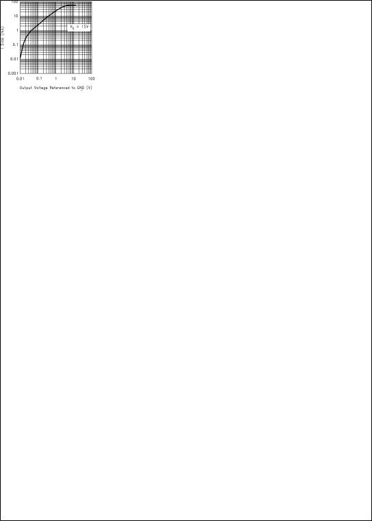
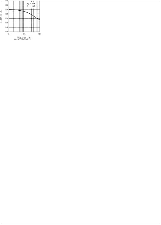
Typical Performance Characteristics VS = +15V, Single Supply, TA = 25ÊC unless otherwise specified
Supply Current vs |
Input Current vs |
Sourcing Current vs |
Supply Voltage |
Temperature |
Output Voltage |
DS011713-40 |
DS011713-41 |
DS011713-42 |
|
Sourcing Current vs |
Sourcing Current vs |
Sinking Current vs |
Output Voltage |
Output Voltage |
Output Voltage |
DS011713-43 |
DS011713-44 |
DS011713-45 |
www.national.com |
6 |
Typical Performance Characteristics VS = +15V, Single Supply, TA = 25ÊC unless otherwise specified (Continued)
Sinking Current vs |
Sinking Current vs |
Output Voltage Swing vs |
Output Voltage |
Output Voltage |
Supply Voltage |
DS011713-46 |
|
DS011713-47 |
|
|
DS011713-48 |
Input Voltage Noise |
Input Voltage Noise |
Input Voltage Noise |
vs Frequency |
vs Input Voltage |
vs Input Voltage |
DS011713-49 DS011713-50 DS011713-51
Input Voltage Noise |
Crosstalk Rejection |
vs Input Voltage |
vs Frequency |
DS011713-52
DS011713-53
7 |
www.national.com |
 Loading...